True Differential Superconducting On-Chip Output Amplifier
Abstract
The true-differential superconductor on-chip amplifier has complementary outputs that float with respect to chip ground. This improves signal integrity and compatibility with the receiving semiconductor stage. Both source-terminated and non-source-terminated designs producing 4 mV demonstrated rejection of a large common mode interference in the package. Measured margins are 8.5% on the output bias, and 28% on AC clock amplitude. Waveforms and eye diagrams are taken at 2.9-10 Gb/s. Direct measurement of bit-error rates are better than the resolution limit of 1e-12 at 2.9 Gb/s, and better than 1e-9 at 10 Gb/s.
On-chip output amplifiers convert the aJ signal-energy of superconductor single-flux-quantum (SFQ) logic to levels that can be detected by standard electronics. A design using a series-array of inductively-isolated, DC-biased SQUIDs has proven to be uniquely effective Herr et al. 2007. The design is amenable to distributed amplifier techniques for improved gain-bandwidth product Herr 2010. An output voltage of 2 mV is adequate for direct interface to a high-performance room-temperature LNA at a data rate of 10 Gb/s Herr 2010. These findings have recently been verified independently Takeuchi et al. 2017; Gupta et al. 2019. The only alternative is the SFQ-to-dc converter Likharev and Semenov 1991, a smaller design that produces only 0.5 mV. This is effective at modest data rates, but 1-10 GHz rates require multistage amplification at intermediate temperature stages Gupta et al. 2019.
Reciprocal Quantum Logic (RQL) is an SFQ logic family that is uniquely attractive in terms of power dissipation and latency Herr et al. 2011. RQL is AC powered, which adds a significant constraint to the output link. The AC power delivered at the clock frequency is typically 45-50 dB larger than the output signals. These power levels produce strong interference in the pressure-contact package, where isolation is imperfect. As the output amplifiers have narrow operating margins on the applied dc bias current, interference large enough to shift the bias and will not only obscure the output signal but prevent it from being generated in the first place.
The solution is to make the driver differential. This is common practice in high-speed interconnect due to its rejection of common-mode interference and noise. Transistor-based designs typically produce the differential signals with two independent drivers that contact chip ground. Amplitude and delay must be well-matched, which presents a design challenge. The stacked-SQUID design can be true-differential, meaning that the outputs are floating with respect to chip ground. This is accomplished by wiring out both ends of the series array. The true-differential design rejects common-mode interference and noise on both the output signal and on the bias current.
A 2 mV output amplifier has been used routinely for lab demonstrations up to 3.5 Gb/s using high performance LNAs on the receiving end at room temperature. The circuit converts the SFQ-based data encoding of RQL to return-to-zero (RZ) encoding. An important feature of the output amplifiers described here is conversion to standard non-return-to-zero (NRZ) encoding, which has twice the bandwidth efficiency, enabling 10 Gb/s data rates. These designs produce 4 mV. A future target is direct drive of a differential limiting amplifier (e.g., Hittite HMC750LP4) with improved size, weight, and power (SWAP). We report measurements from a sampling of parts, including 10 GHz operation of a circuit fabricated internally at Northrop Grumman in a Nb-based six-metal-layer integrated circuit process.
I Design
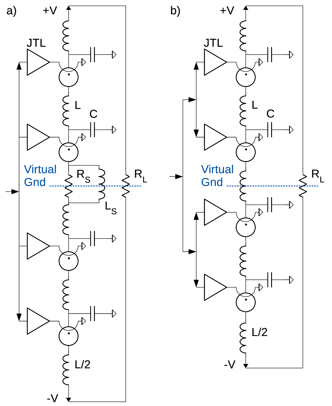
The primary design trade-off is between source-terminated and non-source-terminated. The non-source-terminated circuit is half the size and twice as efficient. However, source termination is required to scale to the higher power-gain product of distributed amplifiers, and to terminate the large signal reflections at the receiving end typical of low-noise LNAs.
As shown in Fig. 1, both designs consist of a series array of SQUIDs connected by an network, as with the previously reported distributed amplifier Herr 2010. The stack is DC-biased with current flowing from the +V to -V nodes. Each SQUID is a low-impedance, floating voltage source producing a sub-mV level. These voltages sum at the output. The lumped inductance and capacitance at every stage produces a filter matched in frequency (and impedance) to the output waveform, and mismatched to the internal oscillatory modes in the SQUID and between multiple SQUIDs. This is the essential function of inductive isolation Herr et al. 2007.
The source-terminated design is effectively two single-ended distributed amplifiers placed back-to-back. Signal propagation time of per stage produces a distributed design that exceeds the bandwidth-gain product of the individual stages. By timing the trigger for each stage, the total rise time can be as small as that of a single stage. The differential signals generated in the array or reflected off the load are equal in amplitude and of opposite polarity as seen by the source termination. This produces a virtual ground, without explicit grounding. The bypass inductor eliminates power dissipation of the bias current. To prevent distortion, the time constant must be large enough to outlast DC offsets that occur in the data pattern, e.g. in a long series of “all-1’s” or “all-0’s”.
The non-source-terminated design produces the same output voltage with half the number of stages. This design also has a virtual ground across the central inductor, but here differential signals will be reflected, not terminated. Without source termination, the design is not amenable to the sequential timing of the distributed amplifier. Instead, the fastest risetime comes by triggering the stack broadside. While this limits the gain-bandwidth product, the design is efficient for modest data rates and output amplitudes.

Here we report two circuits designed to produce 4 mV with 50 ps risetime, supporting data rates of 10 Gb/s. Both circuits convert RQL data encoding to standard NRZ-encoded data at the output, with a fundamental frequency that is half the data rate. As shown in Fig. 2, the conversion is done using a four-junction SQUID that couples signals in through two independent transformers. The RQL pattern applied to the left is delayed by half a cycle and reapplied on the right. The sum of these two return-to-zero (RZ) voltage waveforms produces an NRZ waveform. The design uses two separate JTL networks to feed the output. The feeding JTL and the SQUID are isolated from each other using an unpowered junction. This isolation reduces AC power leakage from JTLs to the SQUID, and reduces back-action from a selected SQUID to the JTLs. A flux bias produces the desired symmetric double-well potential so that the unpowered junction can be triggered.
Advantages of the four-junction SQUID over a conventional two-junction design include: 1) Smaller junctions and larger inductors in the SQUID produce more efficient transformer coupling. These designs did not use holes in the ground plane under the transformers in physical layout. 2) More junctions in the SQUID improves current compliance. Total critical current of 400 A produced the necessary 40 A output signal swing, corresponding to 4 mV into the 100 differential load.
The disadvantage of the four-junction SQUID is relatively modest voltage, 0.25-0.30 mV per stage using Josephson junctions with critical current density of 100 A/m2. With two inputs, the SQUID is only ever partially selected. As illustrated in Fig. 2 by the start-up switching order of the junctions, the selected side of the compound SQUID effectively drives fanout to the other side.
| Output | Source | SQUID | Area | Power | Output | Effcy |
| (mV) | Term | () | (m2) | (nW) | (nW) | (%) |
| 2∗ | No | 8 | 8k | 40 | 10 | 20 |
| 4 | No | 16 | 61k | 160 | 80 | 33 |
| 4 | Yes | 32 | 190k | 320 | 80 | 16 |
| 8 | Yes | 64 | 240k | 1280 | 320 | 16 |
| ∗This amplifier produces RZ output. All others, NRZ. | ||||||
Only the two junctions on the ends of the four-junction SQUID are resistively shunted. As reported earlier Herr et al. 2007; Herr 2010 such creative damping increases the output voltage and the reliability of the transition back to zero. Total damping is mV where is the local parallel shunt resistance and is the total critical current of the SQUID. This is well above the critical damping value of 0.7 mV. However, the whole stack is also shunted by load resistance and source termination resistors, with a total effective damping of mV, This approximates critical damping. Simulated margins on the dc bias of the SQUID stack are about 10%.
The 4 mV design balances speed, output amplitude, and chip area. Parameters of the 4 mV design, in comparison to 2 mV and 8 mV, are given in Table 1. RQL output amplifiers are quite efficient with on-chip power dissipation on a nW-scale, which is negligible compared to the heat load of the cabling. On-chip area of 61k m2 is dominated by that JTL feed network, and is subject to further miniaturization in advanced fabrication processes. Even the largest design is about the same area as that of the associated signal and ground pads in the current package.
II Measurements
All test circuits had a differential input transformer and JTL chain Herr et al. 2011 connected to the output amplifier. Circuits were powered using a resonant network that provisioned the active area of each chip Talanov and Strong 2017.
True-differential output amplifiers have been used on nearly all RQL digital designs, so various configurations, clock frequencies, and fabrication processes have been exercised. The circuits presented here were fabricated either in the process supplied by D-Wave Berkley et al. 2010, or using the “RQL25” process developed internally at Northrop Grumman. Both processes have six metal layers and Josephson junctions with 100 A/m2 critical current density, and support similar layout style with 0.25 m minimum feature size.


The output amplifiers were tested using the channel shown in Fig. 3. The room-temperature LNAs used to amplify the on-chip signal have a typical VSWR specification of 2:1, meaning up to half the signal amplitude is reflected. For the non-source-terminated circuits, 3 dB attenuators were used to improve the impedance match at the expense of cutting the signal-to-noise ratio in half. These attenuators were not used for the source-terminated circuits.


Here we present measurements of waveforms, eye diagrams, and bit-error-rates (BER). Waveform captures are useful as an initial test of signal integrity, as clock and data feed-through, and signal reflections are visible by inspection. Eye diagrams are useful to characterize bandwidth and signal-to-noise of the output data link as a whole. Direct measurements of BER are required to detect switching errors in the output amplifier. This is particularly motivated by the history of elevated switching errors associated with superconducting latching logic and output amplifiers Fulton and Dynes 1971; Suzuki et al. 1988. Underlying each voltage waveform is a large, integral number of SFQ pulses, and sometimes the circuit cannot “decide” exactly how many pulses to produce. This is a manifestation of Buridan’s Principle Lamport 2012.
Fig. 4 shows the measured waveform of a 4 mV source-terminated output amplifier at 3.5 Gb/s. The data show good signal integrity without clock feed-through, confirming effectiveness of the true-differential design. This compares quite favorably to previous results with a single-ended output, where the clock feed-through was as large as the signal Herr et al. 2013.
Fig. 5 shows the measured output amplitude, waveform and eye diagram of the 4 mV non-source-terminated circuit at 2.9 Gb/s. Output amplitude depends on the DC bias current applied to the SQUID stack. The peak-to-peak voltage after amplification is 0.10 V at the nominal bias of 0.30 mA. Bias margins of 8.5% are measured for output voltage within 20% of nominal. Margins on the AC clock that powers the JTL feed network were measured to be 5.0 dB, or 28% in amplitude. This agrees with simulation. The waveform shows good signal integrity, without clock feed-through. The eye diagram at 2.9 Gb/s shows good performance, as BER is directly measured down to 1e-8 and extrapolated down to 1e-15. Additional direct measurements of BER using the PRBS15 pattern found the data link to be error-free down to the resolution limit, 1e-12.
Fig. 6 shows the measured waveform and eye diagram of the same 4 mV non-source-terminated design, but now clocked at 9.95 Gb/s. The waveform again shows good integrity without clock feed-through, but shows reduced amplitude for the standalone “101” token, attributable to an observed risetime of 60 ps, which is a little slower than the 50 ps design value. This token is visible as a secondary rising waveform in the eye diagram. The amplified waveform is clipped by the instrument, as the 2 V peak-to-peak input has an apparent amplitude of about 1.6 V peak-to-peak in the eye diagram. Despite this test artifact, BER was directly measured down to 1e-9.
III Conclusion
The 4 mV true-differential output amplifier achieves low BER for direct-to-room-temperature data rates up to 10 Gb/s, in the presence of large common-mode interference in the package. Measured margins of 8.5% on the output bias and 28% on AC clock amplitude indicate that this component will not limit the performance of larger digital designs. Design trades exist depending on rate, signal amplitude, and the input impedance match at the receiving second-stage amplifier. The simpler non-source-terminated design can be used where explicit attenuation is added to the LNA inputs to improve the impedance match, but this comes at the expense of reduced signal power. Source termination handles the reflections typical of low-noise LNAs, but requires twice as much voltage generated on chip as only half of signal goes to the load. Source-termination also enables distributed-amplifier designs that scale to higher data rates at higher output amplitude. Direct interface to a second-stage differential limiting amplifier is a goal for the future.
Acknowledgements.
Many people contributed to the design, fabrication, and test of these circuits. We acknowledge James Wise and Deepal Wehella Gamage for design, Chris Kirby for fabrication, Jose Ibarrondo, Mohammed Lateef, Yamil Huertas Morales and Jose Robinson for test support, and Anna Herr for useful discussions.References
- Herr et al. (2007) Q. P. Herr, D. L. Miller, A. A. Pesetski, and J. X. Przybysz, IEEE transactions on applied superconductivity 17, 565 (2007).
- Herr (2010) Q. P. Herr, Superconductor Science and Technology 23, 022004 (2010).
- Takeuchi et al. (2017) N. Takeuchi, H. Suzuki, and N. Yoshikawa, Applied Physics Letters 110, 202601 (2017).
- Gupta et al. (2019) D. Gupta, S. Sarwana, D. Kirichenko, V. Dotsenko, A. E. Lehmann, T. V. Filippov, W.-T. Wong, S.-W. Chang, P. Ravindran, and J. Bardin, IEEE Transactions on Applied Superconductivity 29, 1 (2019).
- Likharev and Semenov (1991) K. K. Likharev and V. K. Semenov, IEEE transactions on applied superconductivity 1, 3 (1991).
- Herr et al. (2011) Q. P. Herr, A. Y. Herr, O. T. Oberg, and A. G. Ioannidis, Journal of applied physics 109, 103903 (2011).
- Talanov and Strong (2017) V. V. Talanov and J. A. Strong, Clock distribution network for a superconducting integrated circuit (2017), US Patent 9,722,589.
- Berkley et al. (2010) A. Berkley, M. Johnson, P. Bunyk, R. Harris, J. Johansson, T. Lanting, E. Ladizinsky, E. Tolkacheva, M. Amin, and G. Rose, Superconductor Science and Technology 23, 105014 (2010).
- Fulton and Dynes (1971) T. Fulton and R. Dynes, Solid State Communications 9, 1069 (1971).
- Suzuki et al. (1988) H. Suzuki, A. Inoue, T. Imamura, and S. Hasuo, in Technical Digest., International Electron Devices Meeting (IEEE, 1988), pp. 290–293.
- Lamport (2012) L. Lamport, Foundations of Physics 42, 1056 (2012).
- Herr et al. (2013) A. Y. Herr, Q. P. Herr, O. T. Oberg, O. Naaman, J. X. Przybysz, P. Borodulin, and S. B. Shauck, Journal of Applied Physics 113, 033911 (2013).