Spin Wave Based Approximate Computing
Abstract
By their very nature Spin Waves (SWs) enable the realization of energy efficient circuits as they propagate and interfere within waveguides without consuming noticeable energy. However, SW computing can be even more energy efficient by taking advantage of the approximate computing paradigm as many applications are error-tolerant like multimedia and social media. In this paper we propose an ultra-low energy novel Approximate Full Adder (AFA) and a -bit inputs Multiplier (AMUL). The approximate FA consists of one Majority gate while the approximate MUL is built by means of AND gates. We validate the correct functionality of our proposal by means of micromagnetic simulations and evaluate the approximate FA figure of merit against state-of-the-art accurate SW, CMOS, Spin Hall Effect (SHE), Domain Wall Motion (DWM), accurate and approximate CMOS, Magnetic Tunnel Junction (MTJ), and Spin-CMOS FA implementations. Our results indicate that AFA consumes % and % less energy than state-of-the-art accurate SW and CMOS FA, respectively, and saves % and % when compared with accurate and approximate CMOS, respectively, and provides a orders of magnitude energy reduction when compared with accurate SHE, accurate and approximate DWM, MTJ, and Spin-CMOS, counterparts. In addition, it achieves the same error rate as approximate CMOS and Spin-CMOS FA whereas it exhibits % less error rate than the approximate DWM FA. Furthermore, it outperforms its contenders in terms of area by saving at least % chip real-estate. AMUL is evaluated and compared with state-of-the-art accurate SW and CMOS accurate and approximate state-of-the-art designs. The evaluation results indicate that it saves at least x and x energy in comparison with the state-of-the-art SW designs and CMOS accurate and approximate designs, respectively, and has an average error rate of %, while the approximate CMOS MUL has an average error rate of %, and requires at least % less chip real-estate.
I Introduction
While in the last decades CMOS downscaling has been able to enable high performance computing platforms required to process the information technology revolution induced huge data amount Shah, Steyerberg, and Kent 2018, it becomes very difficult to keep the same downscaling pace due to Haron and Hamdioui 2008: (i) leakage wall, (ii) reliability wall, and (iii) cost wall. This predicts that Moore’s law will come to the end soon and, as a result, researchers have started to explore different technologies (e.g., memristors Yu et al. 2020; Vourkas, Stathis, and Sirakoulis 2018; Maestro-Izquierdo et al. 2019; Pouyan, Amat, and Rubio 2018, graphene devices Jiang et al. 2019; Banadaki and Srivastava 2015; Nishad and Sharma 2015, and spintronics Agarwal et al. 2018; Zabihi et al. 2019; Bai et al. 2018; Vyas et al. 2021) among which Spin Wave (SW) stands apart as one of the most promising due to its Mahmoud et al. 2020; Barman et al. 2021; Mahmoud et al. 2021a; Mahmoud et al. 2020a; Mahmoud et al. 2021b; Mahmoud et al. 2020b; Mahmoud et al. 2020c: (i) Ultra-low energy consumption - SW computing depends on wave interference instead of charge movements. (ii) Acceptable delay. (iii) Highly scalable - SW wavelengths can reach the nanometer range.
Driven by this potential to build energy efficient circuits, several SW based logic gates and circuits have been reported Kostylev et al. 2005; Schneider et al. 2008; Lee and Kim 2008; Ustinova et al. 2017; Mahmoud et al. 2020; Mahmoud et al. 2020a; Mahmoud et al. 2021b; Mahmoud et al. 2020b; Mahmoud et al. 2020c; Fischer et al. 2017; Talmelli et al. 2020; Ciubotaru et al. 2018; Khitun and Wang 2011; Mahmoud et al. 2021a; Gertz et al. 2015. The Mach-Zehnder interferometer was utilized to build a SW NOT gate, which is considered as the first SW computing device Kostylev et al. 2005. Moreover, XNOR, (N)AND, and (N)OR gates were reported by making use of the Mach-Zehnder interferometer Schneider et al. 2008; Lee and Kim 2008; Ustinova et al. 2017. Whereas the Mach-Zehnder interferometer utilise SW amplitude to perform the logic operations, other devices utilize SW phase or both phase and amplitude to build fanout enabled Majority, (N)AND, (N)OR, and X(N)OR gates Mahmoud et al. 2020; Mahmoud et al. 2020b; Mahmoud et al. 2020c. Moreover, SW frequency was utilised as an additional parameter to improve data storage and computing capabilities of multi-frequency Majority and X(N)OR gates Mahmoud et al. 2020a; Mahmoud et al. 2021b. In addition, physical realization of Majority gates were demonstrated Fischer et al. 2017; Talmelli et al. 2020; Ciubotaru et al. 2018. Furthermore, SW circuits were proposed at conceptual level, i.e., without simulation or experimental results, Khitun and Wang 2011, at simulation level, -bit inputs SW multiplier Mahmoud et al. 2021a and magnonic half-adder Wang et al. 2020, as well as simulation based practical range prototypes Gertz et al. 2015.
All the aforementioned logic gates and circuits were designed to provide accurate results, whereas many current applications like multimedia processing and social media are error tolerant and, within certain bounds, are not fundamentally perturbed by computation errors Mittal 2016. Therefore, such applications can benefit from approximate computing circuits, which can save significant amounts of energy, delay, and area, while providing acceptable accuracy. In view of this, this paper introduces novel energy efficient Approximate SW-based Full Adder (AFA) and Approximate -bit inputs Multiplier (AMUL), and its main contributions can be summarized as follows:
- •
Developing and designing a SW based approximate FA: The proposed adder consists of one Majority gate and has a % error rate.
- •
Developing and designing a SW based Approximate -bit inputs MUL: The proposed AMUL is implemented using AND gates and has a % error rate.
- •
Validation of the proposed AFA and AMUL circuits by means of the MuMax3 software.
- •
Demonstrating the superiority: The proposed approximate circuits performance is assessed and compared with accurate and approximate state-of-the-art design counterparts. Our results indicate that AFA consumes % and % less energy than accurate state-of-the-art SW and CMOS counterparts, respectively, and saves % and % in comparison with accurate and approximate CMOS, respectively. In addition, it saves more than orders of magnitude in terms of energy when compared with accurate Spin Hall Effect (SHE) and Domain Wall Motion (DWM), accurate and approximate Magnetic Tunnel Junction (MTJ), and Spin-CMOS based counterparts. In addition, it achieves the same error rate as approximate CMOS and Spin-CMOS FAs and % less error rate than the approximate DWM. Also, it requires at least % less chip real-estate in comparison with the other state-of-the-art designs. Moreover, AMUL saves at least x and x energy in comparison with accurate SW and CMOS accurate/approximate designs, respectively, has an average error rate of %, while the approximate CMOS MUL has an average error rate of %, and requires at least % less chip real-estate.
The paper is organized as follows. Section II provides SW computing background. Section III introduces the proposed approximate circuits. Section IV presents the simulation setup and simulation results. Section V provides performance evaluation data and discusses variability and thermal noise effects and Section VI concludes the paper.
II Spin Wave Based Technology Basics
We explain the SW basics and computing paradigm in this section.
II.1 Spin Wave Fundamentals
The Landau-Lifshitz-Gilbert (LLG) describes the magnetization dynamics caused by the magnetic torque when magnetic material magnetization is out of equilibrium Mahmoud et al. 2020
| (1) |
where is the gyromagnetic ratio, the damping factor, the magnetization, the saturation magnetization, and the effective field which contains the different magnetic interactions. In this work, the effective field is the summation of the external field, the exchange field, the demagnetizing field, and the magneto-crystalline field.
For small magnetic perturbations, Equation (1) can be linearized and results in wave-like solutions which are known as Spin Waves (SWs), which can also be seen as collective excitations of the magnetization within the magnetic material. Just like any other wave, a SW is completely described by its amplitude , phase , frequency , wavelength , and wavenumber . The relation between frequency and wavenumber is called the dispersion relation and is very important for the design of the magnonic devices Mahmoud et al. 2020.
II.2 SW Computation Paradigm
The SW amplitude and phase can be used to encode information at different frequencies, which enables parallelism Mahmoud et al. 2020; Mahmoud et al. 2020a. The interaction between multiple SWs present in the same waveguide is based on the interference principle. Figure 1a) presents an example of interaction between SWs excited with the same , , and in the same waveguide. If the SWs have the same phase , they interfere constructively resulting in a SW with higher amplitude, whereas if they are out of phase , they interfere destructively, resulting in approximately zero amplitude SW. Moreover, SWs interference provides natural support for Majority function evaluation as if an odd number of SWs interfere the resultant SW is obtained by a Majority decision. For example, if same , , and SWs interfere the resultant SW has a phase of if at most SW has a phase of and a phase of if at most SW has a phase of . Note that such a -input Majority CMOS implementation requires transistors whereas in SW technology it is implemented using one waveguide only. More complex interference cases exist if the propagating SWs have different , , and , which might be of interest for designing novel magnonic computing systems. However, in this paper, we focus on the simplest case where all the excited SWs have the same , , and and can take two discrete phases and . Logic refers to a SW with , and a logic refers to a SW with .
Figure 1b) presents a generic SW logic device that consists of four regions: Excitation Stage , Waveguide , Functional Region , and Detection Stage Mahmoud et al. 2020. In SWs are generated by means of, e.g., microstrip antennas Mahmoud et al. 2020, magnetoelectric cells Mahmoud et al. 2020, Spin Orbit Torque Mahmoud et al. 2020. is the medium for SW propagation and can be made of different magnetic materials, e.g., Permalloy, Yttrium iron garnet, CoFeB Mahmoud et al. 2020. The waveguide material is an important parameter as it fundamentally determines the SW properties. In SWs can be amplified, normalized or interfere with other SWs. In the output SW is captured and converted to the electrical domain using the same type of cells as in . Two main SW detection techniques are in place Mahmoud et al. 2020: phase and threshold based. In phase detection, the output is determined by comparing the detected SW phase with a predefined phase. For example, if the detected SW has a phase of / the output is logic /, respectively. Threshold detection determines the output by comparing the detected SW amplitude with a predefined threshold. For instance, if the detected SW amplitude is larger than the predefined threshold, the output is logic and logic otherwise.
| 1 | |||
| 0 |
III SW Approximate Functions
In this section, we introduce and analyse SW-based Approximate Full Adder (AFA) and -bit inputs Multiplier (AMUL).
III.1 SW Approximate Full Adder
Figure 2 presents the proposed Approximate FA (AFA) structure, which has inputs , , and , and outputs and and is a -input Majority gate that evaluates as suggested in Angizi et al. 2018. AFA generates without any error as it is detected as the Majority of , , and , which is also the case in accurate FAs. On the other hand, is detected with a % error rate as approximate the accurate FA Sum, which equals to . Table I presents FA and AFA truth tables, which clarifies that the approximate FA sum is erroneous when all inputs are /.
To achieve the AFA behaviour the design in Figure 2 has to be properly dimensioned. The waveguide width must be smaller or equal to the SW wavelength and SW amplitude, wavelength, and frequency must be the same at every excitation cell. Furthermore, the structure dimensions must be precisely determined because the interference pattern depends on the location and distances between different excitation and detection cells. For example, if the constructive interference pattern is desired when the SWs have the same phase and destructive when the SWs are out-of-phase , , , and must be equal with (where ). In addition, if the inverted Majority is of interest, which is the case for , must be and if the non-inverted output is required, which is the case for , must be . The AFA operation principle relies on a combined process of SWs propagation and interferences as follows: First, SWs are excited at and and propagate diagonally until they interfere constructively or destructively depending on their phases at the connection point. Then, the resulting SW propagates and interferes constructively or destructively with the SW excited at at the next connection point. This interference result generates the final SW, which travels toward the outputs and is detected at and at .
| 0 | |||||||
| 0 | |||||||
| 0 | |||||||
| 1 | |||||||
| 0 | |||||||
| 1 | |||||||
| 1 | 1 |
III.2 SW Approximate -bit inputs Multiplier
Figure 3 presents the proposed Approximate -bit inputs SW-based Multiplier (AMUL). Its inputs are the -bit operands and and its -bit output is . AMUL consists of AND gates, which evaluate the AMUL outputs as , , and , excitation cells, and detection cells.
To evaluate the error rate we note that in the accurate MUL the outputs bits are computed as , , , and , and present in Table 2 MUL and AMUL output values for all possible input combinations. Note that the erroneous values are written in bold and underlined. One can observe in the Table that AMUL computes without any error, and , , and with %, %, and % error rate, respectively. However if threshold based output detection is utilized the error rate for and can be reduced to % and %, respectively, as demonstrated in Section IV, which brings our proposal to an average error rate of %.
The previously mentioned design parameters hold true for the AMUL as well. However, in contrast to AFA, AMUL relies on threshold based output detection, which means that the detection cells must be as close as possible to the last interference point, thus , , , and should be minimized.
IV Simulation Setup and Results
The simulation setup and simulation results are provided and explained in this section.
IV.1 Simulation Setup
We make use of a width and thick waveguide and the parameters specified in Table 3 Devolder et al. 2016 to validate the proposed approximate designs (AFA and AMUL) by means of MuMax3 Vansteenkiste et al. 2014. As previously mentioned, the SW wavelength should be larger than the waveguide width to improve the interference pattern. Therefore, a SW wavelength was chosen. After that, the AFA dimension are determined as follows: =, =, =, =, and = and the AMUL are =, =, =, =, =, =, and =. Last, based on the SW dispersion relation, the SW frequency for a wavenumber == was calculated to correspond to a SW frequency of .
| Parameters | Values |
|---|---|
| Saturation magnetization | A/m |
| Perpendicular anisotropy constant | MJ/ |
| Damping constant | |
| Exchange stiffness | pJ/m |
IV.2 Simulation Results
-bit approximate FA based on phase detection
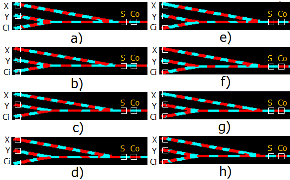
Figure 4 a) to h) present AFA MuMax3 simulation results for {,,}= {,,}, {,,}, {,,}, {,,}, {,,}, {,,}, {,,}, {,,}, and {,,}, respectively. Note that blue represents logic and red logic . One can observe in the Figure that the outputs and are detected as expected. For instance, for {,,}= {,,}, {,,}, {,,}, and {,,}, while for {,,}= {,,}, {,,}, {,,}, and {,,}. Moreover, is inverted as expected.
-bit inputs approximate MUL based on threshold detection
Figures 5 to 8 present AMUL MuMax3 simulation results. In the figures, the -axis presents the SWs over ratio, where is the magnetization projection along the -direction and the saturation magnetization. Inspecting Figure 5 we observe that output SW magnetization at time for the input values ={,,,}, which should corresponds to , is larger than and smaller than for the rest of the input combinations. Thus, by setting the detection threshold to , i.e., SW magnetization larger than means logic and logic otherwise, is always properly detected.
Similarly, one can analyze Figure 6. For instance, the SWs magnetization for the input combinations ={,,,,,,,} are larger than when reading them at time , whereas for the other input combinations magnetization is less than . Therefore, if the threshold is set to value can be derived. Note that by doing so the theoretically predicted error rate of % is diminished to %.
Using the same way, Figure 7 is analyzed. The SW magnetization for input combinations ={,,,} are larger than when reading them at time , whereas for the rest magnetization are less than . Therefore, if the threshold is set to be can be properly obtained with % error rate.
Finally, Figure 8 is analyzed in the same manner. The SWs magnetization for input combination ={} is larger than when reading them at time , whereas the rest of magnetization are less than . Therefore, if the threshold is set to be can be obtained with % error rate.
V Performance Evaluation and Discussion
In this section, the proposed AFA and AMUL are evaluated and compared with the state-of-the-art designs. Furthermore, the variability and thermal noise effects are discussed in addition to some open issues related to SW technology.
Performance Evaluation
To get inside on the practical implications of our proposal we compare AFA with the state-of-the-art accurate SW Mahmoud et al. 2021, CMOS Canan et al. 2019, SHE Roohi et al. 2017, DWM Roohi, Zand, and DeMara 2016, accurate and approximate CMOS Gupta et al. 2011, MTJ Cai et al. 2017, and Spin-CMOS Angizi et al. 2018 counterparts in terms of energy, delay, and area (the number of utilized devices). To evaluate AFA we make use of the following assumptions: (i) Excitation and detection cells are Magnetoelectric (ME) cells which power consumption and delay are and , respectively Zografos et al. 2015. (ii) During propagation and interference, SWs consume negligible amount of energy. (iii) The outputs are driving followup gates, the detection cells are not considered in the energy consumption calculation. (iv) Pulse signals are used to excite SWs. Note that due to SW technology early stage development the aforementioned assumptions might need to be re-evaluated as the SW technology becomes more mature.
The AFA delay is calculated by adding ME cell delay to the SW propagation delay through the waveguide determined by means of micromagnetic simulation and equals to . Table 4 presents the results of the evaluation and comparison. Inspecting the Table, it is clear that AFA outperforms state-of-the-art CMOS Canan et al. 2019 accurate FA by energy reductions of approximately %, while exhibiting more than orders of magnitude larger delay. Furthermore, AFA saves approximately % and % energy while requiring x and x larger delay when compared with CMOS based accurate and approximate FA, respectively, while having the same error rate as the approximate FA in Gupta et al. 2011. When compared with other emerging technologies based designs, AFA consumes orders of magnitude less energy than MTJ based accurate and approximate FAs while exhibiting % lower delay and having % better error rate than the MTJ approximate FA in Cai et al. 2017. Moreover, AFA consumes and orders of magnitude less energy than SHE- and DWM- based accurate FAs, respectively, has x lower and % more delay than SHE Roohi et al. 2017 and DWM Roohi, Zand, and DeMara 2016 based FAs, respectively. Furthermore, AFA consumes approximately and orders of magnitude less energy while requiring % and % lower delay in comparison with the accurate and approximate Spin-CMOS based FAs, respectively, while having the same error rate as the approximate FA in Angizi et al. 2018. Last but not least, AFA outperforms the SW based accurate FA Mahmoud et al. 2021 by % and % in terms of energy and delay, respectively. Note that as a chip real-estate estimation that the proposed approximate FA requires the lowest number of devices.
| Technology | Type | Error Rate | Energy (fJ) | Delay (ns) | Device No. |
|---|---|---|---|---|---|
| CMOS Canan et al. 2019 | Accurate | ||||
| CMOS Gupta et al. 2011 | Accurate | ||||
| CMOS Gupta et al. 2011 | Approximate | ||||
| MTJ Cai et al. 2017 | Accurate | ||||
| MTJ Cai et al. 2017 | Approximate | ||||
| MTJ Cai et al. 2017 | Approximate | ||||
| SHE Roohi et al. 2017 | Accurate | ||||
| DWM Roohi, Zand, and DeMara 2016 | Accurate | ||||
| Spin CMOS Angizi et al. 2018 | Accurate | ||||
| Spin CMOS Angizi et al. 2018 | Approximate | ||||
| Spin Wave Mahmoud et al. 2021 | Accurate | ||||
| Spin Wave | Approximate |
Under the same assumptions AMUL delay is and we compare it with state-of-the-art SW Mahmoud et al. 2021a and CMOS Kulkarni, Gupta, and Ercegovac 2011 counterparts. As delay figures are not mentioned for the approximate multiplier in Kulkarni, Gupta, and Ercegovac 2011, its energy consumption was estimated based on the CMOS figures provided in Chen et al. 2013. Table 5 present the results of the evaluation and comparison. Inspecting the Table, it is clear that AMUL outperforms accurate CMOS Kulkarni, Gupta, and Ercegovac 2011 and approximate CMOS Kulkarni, Gupta, and Ercegovac 2011 counterparts by diminishing the energy consumption by x and x while exhibiting x and x larger delay, respectively. AMUL has an average error rate of % while % is the average error rate for the approximate CMOS counterpart Kulkarni, Gupta, and Ercegovac 2011. Note that the average error rate is calculated by adding the average of , , and error rates as the first output is accurately compute in both implementations. When compared with accurate MUL SW implementations, AMUL saves x and x energy and approximately x lower and x more delay in comparison with SW coupler and conversion based MUL implementations, respectively. We note that the SW propagation delay is neglected into the evaluation of the SW conversion based MUL in Mahmoud et al. 2021a. One can observe from the Table that the proposed MUL requires less ME cells than the SW designs in Mahmoud et al. 2021a which indicates that the design in Mahmoud et al. 2021a has a larger area and by implication a larger delay if SW propagation is also considered.
| Design | CMOSChen et al. 2013; Kulkarni, Gupta, and Ercegovac 2011 | SWMahmoud et al. 2021a | Proposed SW MUL | ||
|---|---|---|---|---|---|
| Implemented method | - | Coupler Cascading | Conversion Cascading | - | |
| Type | Accurate | Approximate | Accurate | Accurate | Approximate |
| Average Error Rate | |||||
| energy (aJ) | |||||
| Delay (ns) | |||||
| Device No. | |||||
Variability and Thermal Effect
In this paper, the main target is to propose and validate by means of micromagnetic simulations the approximate FA and MUL as proof of the concepts without considering the impacts of the thermal noise and the variability. However, it was reported that the thermal noise has limited effect on the gate function and consequently the gate works correctly at different temperature Wang et al. 2018. In addition, the effect of the edge roughness and the waveguide trapezoidal cross section were demonstrated Wang et al. 2018. It was suggested that both effects are very small and the gate operates correctly at their presence as well Wang et al. 2018. Therefore, we don’t expect neither the thermal noise nor the geometrical variability to have large impact on the proposed circuits. However, we plan to investigate these phenomena in the future.
Discussion
Although the evaluation demonstrated that the SW technology has the needed requirements to improve the state-of-the-art in terms of energy as well as area consumption, but a number of open issues are still to be solved Mahmoud et al. 2020:
- •
Immature technology: It seems that the ME cells are the right option to excite and detect the SW because of their ultra low energy consumption, acceptable delay and scalability. However, ME cells are not realized experimentally until now.
- •
Scalability: In terms of area SW circuit have a great scaling potential as for proper functionality SW device dimensions must be greater or equal than the SW wavelength, which can reach down to the range. Several SW circuit area benchmarkings have been reported Zografos et al. 2015 which indicate that hybrid spin-wave–CMOS circuits have very small area. Although the assumptions the benchmarking is based on might not be fully realistic, they give an indication regarding the expected area. For example, the area of a -bit divider (DIV32) implemented in hybrid SW-CMOS is roughly about x smaller than the one of the 10 nm CMOS counterpart. However, few things are needed before being able to realize nano-scale SW device such as excitation and detection: currently, it is not possible to distinguish SWs from noise.
VI Conclusions
We proposed and validated by means of micromagnetic simulations a novel approximate energy efficient spin wave based Full Adder (AFA) and -bit inputs multiplier (AMUL). Both designs were evaluated and compared with the state-of-the-art counterparts. AFA saves % and % energy when compared with the state-of-the-art SW and CMOS, respectively, and % and % in comparison with accurate and approximate CMOS, respectively. In addition, it saves more than orders of magnitude when compared with accurate SHE, and accurate and approximate DWM, MTJ, and Spin-CMOS FAs. Moreover, it achieves the same error rate as approximate CMOS and Spin-CMOS FA whereas it exhibits % less error rate than approximate DWM FA and requires at least % less chip real-estate in comparison with the other state-of-the-art designs. At its turn AMUL saves at least x and x energy in comparison with the state-of-the-art accurate SW designs and CMOS accurate and approximate designs, respectively. Moreover, the AMUL has an average error rate of %, while the approximate CMOS MUL has an average error rate of %, and requires at least % less chip real-estate.
Acknowledgement
This work has received funding from the European Union’s Horizon 2020 research and innovation program within the FET-OPEN project CHIRON under grant agreement No. 801055. It has also been partially supported by imec’s industrial affiliate program on beyond-CMOS logic. F.V. acknowledges financial support from Flanders Research Foundation (FWO) through grant No. 1S05719N.
References
- Shah, Steyerberg, and Kent (2018) N. D. Shah, E. W. Steyerberg, and D. M. Kent, JAMA (2018).
- Haron and Hamdioui (2008) N. Z. Haron and S. Hamdioui, in Design and Test Workshop, 2008. IDT 2008. 3rd International (IEEE, 2008) pp. 98–103.
- Yu et al. (2020) J. Yu, R. Nane, I. Ashraf, M. Taouil, S. Hamdioui, H. Corporaal, and K. Bertels, IEEE Transactions on Emerging Topics in Computing 8, 545 (2020).
- Vourkas, Stathis, and Sirakoulis (2018) I. Vourkas, D. Stathis, and G. H. Sirakoulis, IEEE Transactions on Emerging Topics in Computing 6, 145 (2018).
- Maestro-Izquierdo et al. (2019) M. Maestro-Izquierdo, J. Martin-Martinez, A. C. Yepes, M. Escudero, R. Rodriguez, M. Nafria, X. Aymerich, and A. Rubio, IEEE Transactions on Emerging Topics in Computing 7, 545 (2019).
- Pouyan, Amat, and Rubio (2018) P. Pouyan, E. Amat, and A. Rubio, IEEE Transactions on Emerging Topics in Computing 6, 207 (2018).
- Jiang et al. (2019) Y. Jiang, N. C. Laurenciu, H. Wang, and S. D. Cotofana, IEEE Transactions on Nanotechnology 18, 287 (2019).
- Banadaki and Srivastava (2015) Y. Banadaki and A. Srivastava, IEEE Transactions on Emerging Topics in Computing 3, 458 (2015).
- Nishad and Sharma (2015) A. Nishad and R. Sharma, IEEE Transactions on Emerging Topics in Computing 3, 470 (2015).
- Agarwal et al. (2018) S. Agarwal, G. Burr, A. Chen, S. Das, E. Debenedictis, M. P. Frank, P. Franzon, S. Holmes, M. Marinella, and T. Rakshit, “International roadmap of devices and systems 2017 edition: Beyond cmos chapter.” Tech. Rep. (Sandia National Lab.(SNL-NM), Albuquerque, NM (United States), 2018).
- Zabihi et al. (2019) M. Zabihi, Z. Chowdhury, Z. Zhao, U. R. Karpuzcu, J. Wang, and S. S. Sapatnekar, IEEE Transactions on Computers 68, 1159 (2019).
- Bai et al. (2018) Y. Bai, R. F. DeMara, J. Di, and M. Lin, IEEE Transactions on Computers 67, 631 (2018).
- Vyas et al. (2021) V. Vyas, L. Jiang-Wei, P. Zhou, X. Hu, and J. S. Friedman, IEEE Transactions on Computers 70, 128 (2021).
- Mahmoud et al. (2020) A. Mahmoud, F. Ciubotaru, F. Vanderveken, A. V. Chumak, S. Hamdioui, C. Adelmann, and S. Cotofana, Journal of Applied Physics 128, 161101 (2020), https://doi.org/10.1063/5.0019328 .
- Barman et al. (2021) A. Barman et al., Journal of Physics: Condensed Matter (2021).
- Mahmoud et al. (2021a) A. N. Mahmoud, F. Vanderveken, C. Adelmann, F. Ciubotaru, S. Cotofana, and S. Hamdioui, IEEE Transactions on Circuits and Systems I: Regular Papers 68, 536 (2021a).
- Mahmoud et al. (2020a) A. Mahmoud, F. Vanderveken, F. Ciubotaru, C. Adelmann, S. Cotofana, and S. Hamdioui, in 2020 Design, Automation Test in Europe Conference Exhibition (DATE) (2020) pp. 642–645.
- Mahmoud et al. (2021b) A. N. Mahmoud, F. Vanderveken, C. Adelmann, F. Ciubotaru, S. Hamdioui, and S. Cotofana, IEEE Transactions on Magnetics , 1 (2021b).
- Mahmoud et al. (2020b) A. Mahmoud, F. Vanderveken, C. Adelmann, F. Ciubotaru, S. Cotofana, and S. Hamdioui, in ISVLSI (2020) pp. 60–65.
- Mahmoud et al. (2020c) A. Mahmoud, F. Vanderveken, C. Adelmann, F. Ciubotaru, S. Hamdioui, and S. Cotofana, in 2020 IEEE 38th International Conference on Computer Design (ICCD) (2020) pp. 332–335.
- Kostylev et al. (2005) M. P. Kostylev, A. A. Serga, T. Schneider, B. Leven, and B. Hillebrands, Applied Physics Letters 87, 153501 (2005), https://doi.org/10.1063/1.2089147 .
- Schneider et al. (2008) T. Schneider, A. A. Serga, B. Leven, B. Hillebrands, R. L. Stamps, and M. P. Kostylev, Applied Physics Letters 92, 022505 (2008), https://doi.org/10.1063/1.2834714 .
- Lee and Kim (2008) K.-S. Lee and S.-K. Kim, Journal of Applied Physics 104, 053909 (2008), https://doi.org/10.1063/1.2975235 .
- Ustinova et al. (2017) I. A. Ustinova, A. A. Nikitin, A. B. Ustinov, B. A. Kalinikos, and E. Lähderanta, in 2017 11th International Workshop on the Electromagnetic Compatibility of Integrated Circuits (EMCCompo) (2017) pp. 104–107.
- Mahmoud et al. (2020) A. Mahmoud, F. Vanderveken, C. Adelmann, F. Ciubotaru, S. Hamdioui, and S. Cotofana, AIP Advances 10, 035119 (2020), https://doi.org/10.1063/1.5134690 .
- Fischer et al. (2017) T. Fischer, M. Kewenig, D. A. Bozhko, A. A. Serga, I. I. Syvorotka, F. Ciubotaru, C. Adelmann, B. Hillebrands, and A. V. Chumak, Applied Physics Letters 110, 152401 (2017), https://doi.org/10.1063/1.4979840 .
- Talmelli et al. (2020) G. Talmelli, T. Devolder, N. Träger, J. Förster, S. Wintz, M. Weigand, H. Stoll, M. Heyns, G. Schütz, I. P. Radu, J. Gräfe, F. Ciubotaru, and C. Adelmann, Science Advances 6 (2020), 10.1126/sciadv.abb4042, https://advances.sciencemag.org/content/6/51/eabb4042.full.pdf .
- Ciubotaru et al. (2018) F. Ciubotaru, G. Talmelli, T. Devolder, O. Zografos, et al., in 2018 IEEE International Electron Devices Meeting (IEDM) (2018) pp. 36.1.1–36.1.4.
- Khitun and Wang (2011) A. Khitun and K. L. Wang, Journal of Applied Physics 110, 034306 (2011), https://doi.org/10.1063/1.3609062 .
- Gertz et al. (2015) F. Gertz, A. Kozhevnikov, Y. Filimonov, and A. Khitun, IEEE Transactions on Magnetics 51, 1 (2015).
- Wang et al. (2020) Q. Wang, M. Kewenig, M. Schneider, R. Verba, F. Kohl, B. Heinz, M. Geilen, M. Mohseni, B. Lägel, F. Ciubotaru, et al., Nature Electronics , 1 (2020).
- Mittal (2016) S. Mittal, ACM Comput. Surv. 48 (2016), 10.1145/2893356.
- Angizi et al. (2018) S. Angizi, H. Jiang, R. F. DeMara, J. Han, and D. Fan, IEEE Transactions on Nanotechnology 17, 795 (2018).
- Devolder et al. (2016) T. Devolder, J.-V. Kim, F. Garcia-Sanchez, J. Swerts, W. Kim, S. Couet, G. Kar, and A. Furnemont, Phys. Rev. B 93, 024420 (2016).
- Vansteenkiste et al. (2014) A. Vansteenkiste, J. Leliaert, M. Dvornik, M. Helsen, F. Garcia-Sanchez, and B. Van Waeyenberge, AIP Advances 4, 107133 (2014), https://doi.org/10.1063/1.4899186 .
- Mahmoud et al. (2021) A. Mahmoud, F. Vanderveken, F. Ciubotaru, C. Adelmann, S. Cotofana, and S. Hamdioui, “Spin wave based full adder,” (2021), arXiv:2102.08108 [cond-mat.mes-hall] .
- Canan et al. (2019) T. F. Canan, S. Kaya, A. Karanth, and A. Louri, IEEE Journal on Exploratory Solid-State Computational Devices and Circuits 5, 94 (2019).
- Roohi et al. (2017) A. Roohi, R. Zand, D. Fan, and R. F. DeMara, IEEE Transactions on Computer-Aided Design of Integrated Circuits and Systems 36, 2134 (2017).
- Roohi, Zand, and DeMara (2016) A. Roohi, R. Zand, and R. F. DeMara, IEEE Transactions on Magnetics 52, 1 (2016).
- Gupta et al. (2011) V. Gupta, D. Mohapatra, S. P. Park, A. Raghunathan, and K. Roy, in IEEE/ACM International Symposium on Low Power Electronics and Design (2011) pp. 409–414.
- Cai et al. (2017) H. Cai, Y. Wang, L. A. De Barros Naviner, and W. Zhao, IEEE Transactions on Circuits and Systems I: Regular Papers 64, 847 (2017).
- Zografos et al. (2015) O. Zografos, B. Sorée, A. Vaysset, S. Cosemans, L. Amarù, P. Gaillardon, G. De Micheli, R. Lauwereins, S. Sayan, P. Raghavan, I. P. Radu, and A. Thean, in 2015 IEEE 15th International Conference on Nanotechnology (IEEE-NANO) (2015) pp. 686–689.
- Kulkarni, Gupta, and Ercegovac (2011) P. Kulkarni, P. Gupta, and M. Ercegovac, in 2011 24th Internatioal Conference on VLSI Design (2011) pp. 346–351.
- Chen et al. (2013) Y. Chen, A. Sangai, M. Gholipour, and D. Chen, in 2013 IEEE/ACM International Symposium on Nanoscale Architectures (NANOARCH) (2013) pp. 82–88.
- Wang et al. (2018) Q. Wang, P. Pirro, R. Verba, A. Slavin, B. Hillebrands, and A. V. Chumak, Science Advances 4 (2018), 10.1126/sciadv.1701517, https://advances.sciencemag.org/content/4/1/e1701517.full.pdf .