A
The SpiNNaker 2 Processing Element Architecture for Hybrid Digital Neuromorphic Computing
Abstract
This paper introduces the processing element architecture of the second generation SpiNNaker chip, implemented in 22nm FDSOI. On circuit level, the chip features adaptive body biasing for near-threshold operation, and dynamic voltage-and-frequency scaling driven by spiking activity. On system level, processing is centered around an ARM M4 core, similar to the processor-centric architecture of the first generation SpiNNaker. To speed operation of subtasks, we have added accelerators for numerical operations of both spiking (SNN) and rate based (deep) neural networks (DNN). PEs communicate via a dedicated, custom-designed network-on-chip. We present three benchmarks showing operation of the whole processor element on SNN, DNN and hybrid SNN/DNN networks.
Index Terms:
MPSoC, neuromorphic computing, SpiNNaker2, power management, DVFS, synfire chainI Introduction
Neuromorphic circuits try to mimic certain aspects of neural tissue [1]. The aim is to further our understanding of how the brain computes information, as well as derive novel types of computational hardware for e.g. artificial intelligence applications [2, 3]. This paper introduces the processing element (PE) architecture of the second generation SpiNNaker chip, a digital neuromorphic system. The ”Spiking Neural Network Architecture” SpiNNaker is a processor platform optimized for the simulation of neural networks [4]. A large number of Arm processor cores is integrated in a system architecture optimized for communication and memory access. Specifically, to take advantage of the asynchronous, naturally parallel and independent sub-computations of biological neurons, each core simulates neurons independently and communicates via a lightweight, spike-optimized asynchronous communication protocol.
The second generation SpiNNaker2 scales down technology from 130nm CMOS to 22nm FDSOI CMOS [5], while also introducing a number of new features. Adaptive body biasing (ABB) in this 22nm FDSOI process node delivers cutting-edge power consumption [6]. With dynamic voltage and frequency scaling, the energy consumption of the PEs scales with the spiking activity computed on the cores [7, 8]. The Arm Cortex-M4 cores employed for SpiNNaker2 integrate a single-precision floating point unit, thus extending the fixed-point arithmetic of the first generation SpiNNaker. Computation-wise, SpiNNaker2 retains the processor-based flexibility of the first generation system [9], while adding additional numerical accelerators to speed up common operations [10, 11, 12]. In the current prototype described in this paper, another accelerator has been added, a 16 by 4 array of 8 bit multiply-accumulate units (MAC), enabling faster 2D convolution and matrix-matrix multiplication [13]. Efficient usage of these accelerators can extend the simulation capacity of SpiNNaker2 by a significant factor [14]. The PEs are arranged in groups of four to quad-processing-elements (QPEs) which are connected by a Network-on-Chip (NoC) to allow scaling towards a large neuromorphic System-on-Chip (SoC).
In the following, we introduce the processing element architecture of SpiNNaker2. Subsequently, we show results from the current prototype, specifically a side-by-side implementations of (1) a conventional spiking neural network using the numerical accelerators (2) a standard DNN layer using the MAC array and (3) a hybrid network, where we use the MAC in a spiking context.
II Hybrid Neuromorphic Computation Approach
We try to capture our approach to neuromorphic computing with the term ”hybrid”. In a general sense, this means we aim to achieve a compromise between (a) the software/processor-based approach of Loihi [15] and the first generation SpiNNaker [16] and (b) the classical neuromorphic approaches with dedicated neuron and synapse circuits (in digital or analog) [17, 18, 19, 20]. Thus, while we do not implement the full neuron and synapse functionality as dedicated circuits, we aim to achieve close to this kind of efficiency by numerically accelerating common operations such as exponentials, log or random functions. At the same time, classical neuromorphic approaches have always been hindered by their essential hard-coding of functionality, which we aim to avoid by keeping the processor cores at the center, employing them to tie the accelerator blocks together.
In an extension of the above definition, ”hybrid” also means that we can realize both spiking and rate-based artificial neural networks (SNN/ANN) on SpiNNaker2, since we incorporated accelerators for both types of networks and the ARM processors and communication infrastructure (Network on chip, DMA, etc) are flexible enough to support both. Thus, hybrid networks at the boundary between SNNs and ANN can be realized that combine the best of both worlds, e.g. the numerical simplicity of ANNs with the sparsity and time-dynamic features of SNNs, for enhanced energy efficiency and novel computational paradigms. In a specific instantiation of this idea, the MAC array could be run not frame-based, but in an event-triggered fashion. To fully use the multipliers, this mode of operation needs a graded weight (usually given) and a graded activity-related input value (usually not given, if we assume single-bit axonal spikes). Biologically realistic versions of a graded input value (i.e. multi-bit spikes) for the multipliers in the MAC array could be (1) electrical synapses that generally transmit graded values, e.g. in a retina model. (2) Dendritic computation, i.e. where amplitudes inside a neuron are scalar and have some amplification factor (weight) when being transmitted to other parts of the neuron. Or (3) treating the neuron input as a scalar synaptic current (e.g. representing a pixel grayscale value). This approach is employed in our hybrid use case later in the paper. Non-biologically realistic versions would use the possibility of a ‘spike with a payload’ for e.g. more efficient coding by trading spike payload for spike frequency, achieving increased sparsity [21]. Another possibility could be more complex processing. That is, the payload could represent some dynamic characteristic of the neuron, e.g. the value of some adaptation process, or how fast the charging slope was, etc.
III SpiNNaker 2 Many-Core Architecture
With the shrink of semiconductor technologies more processing elements (PEs) can be integrated on a single silicon die, which improves scalability toward multi-million core neuromorphic processors systems. However, the on-chip bus system (system NoC) from SpiNNaker [9] does not scale toward a larger number of on-chip PEs, since it is implemented with flat logic on the chip top-level. This approach is not feasible for a larger number of PEs since flat top-level routing and timing closure would not be feasible. Therefore a quad-processing element (QPE) architecture is employed here, as described in the following.
III-A QPE and NoC Architecture

Fig. 1 shows the top-level floorplan architecture of SpiNNaker 2. Its main components are 38 QPEs with 152 PEs in total. The SpiNNaker 2 packet router (Sec. III-B) is responsible for spike communication. In total 6 chip-to-chip communication links allow to form the SpiNNaker multichip network [9]. A host interface allows to connect to an Ethernet infrastructure. Two LPDDR4 memory controllers and PHYs allow the connection of off-chip DRAM. A periphery block contains various low-speed interfaces (GPIO, JTAG, SPI) for configuration, debugging and other general purpose use cases.
A detailed view of the QPE is shown in Fig. 2. The QPE logically combines 4 PEs and a NoC router, with connections to the PEs and the four neighbor QPEs. It is implemented in a globally-asynchronous-locally-synchronous (GALS) clocking scheme, allowing the PEs to operate in the dynamic voltage and frequency scaling (DVFS) scheme from [8] independent from each other and the NoC router logic. Additionally, the GALS approach also decouple the QPEs from each other to prevent the need for a chip top-level synchronous clock distribution network. Therefore, the QPE further forms a place and route hard macro which can be seamlessly arranged in an array on chip top-level to build a the many-core SoC. All signal connections to neighbor QPEs are realized in a connect-by-place scheme with asynchronous FIFO clock domain crossings. Additionally ot the NoC connections, only a small number of dedicated signals are routed between the QPEs, as for example clock, reset and a few physical interrupt signal lines. The NoC is the main communication resource that interconnects all on-chip components in a 2D-mesh structure. It consists of two independent but interconnected NoC meshes: the data NoC (DNoC) and configuration NoC (CNoC). For data transfers such as DMA or spike packets the DNoC is used. A simplified structure of the NoC router is shown in Fig. 3. It consists of wide asynchronous FIFOs for synchronous incoming packets to the router’s clock domain. The packet destination is determined by a X/Y-first routing logic. A following FIFO stage is shorten the internal critical timing path. The output port control arbitrates incoming routing requests in a round-robin fashion and controls the crossbar accordingly. DNoC flit size is 192bit hence an entire packet can transferred at once for high throughput. The router’s latency is 5 clock cycles per hop at a frequency of 400MHz. Besides the NoC a separated CNoC is implemented. It is operated using the reference clock signal and is thereby operational if no clock generator is switched on. And provides access to all registers in a boot-up and configuration step. During operation it allows for data transmission, even if the DNoC is blocked, e.g. by large DMAs. It has a flit width of 32bit and is operating in a worm-hole switching scheme. For interoperability DNoC and CNoC are using the identical packet format shown in 4. The 192bit NoC packet consists of a 15bit NoC header, 17bit packet header, 32bit address and 0 up-to 128bit payload data. Routing decisions of the NoC are made based on the X/Y destination coordinates of the NoC packet. Additionally there are four destination PE bits reserved to allow a multicast on QPE level for spike packet or data packets.
Within SpiNNaker2 mainly data packets and SPiNNaker packets (see Sec. III-B) are transmitted. The NoC allows to abstract communication to the PEs also for infrastructure signals. This includes interrupt packets or dedicated test data streams for scan tests of the PEs.

III-B The SpiNNaker Router
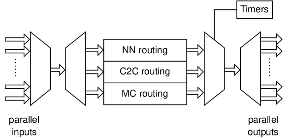
The SpiNNaker2 packet router, based on [22, 23], is one of the key components of the chip. It is responsible for routing multicast, core-to-core and nearest neighbour packets. An overview of the SpiNNaker2 packet router architecture is shown in Fig. 5. The router incorporates a number of evolutions to support the increased communication throughput, such as parallel routing structure, larger multicast routing tables, improved packet-dropping mechanism, out-of-order issue buffer and a large optional packet payload. Error Correction Code (ECC) SRAMs are adopted and TCAM built-in self-test is designed to improve fault tolerance and test automation. Additionally, the router has fully payload pipeline control and a clock gating implementation for power-saving. The multicast packets are used for neural events and routed by a key provided at the source. The core-to-core packets are routed by a destination address to any core on any chip and intended for machine management. Last but not least, the nearest neighbour packets are routed by destination port(s) to the monitor processor(s) of the neighbouring chip(s), and they are intended for machine boot and debugging functions. The packet format is shown in Fig. 6.

III-C Processing Element
As shown in Fig. 7, the processing Element (PE) consists of the Arm Cortex-M4F core, pseudo and true random number generators [12], a fixed-point exponential and logarithm accelerator [10, 11], a MAC array, timers, SRAM memory array, AHB bus, DMA, and crossbar. DVFS [8] allows for switching between two VDD rails (PL1 and PL2 in Fig. 7) during operation of the PE.
While the Arm core forms the main computational resource of the PE, the additional accelerators like the random number generators and the MAC array can greatly increase the computational and power efficiency for certain applications [24][14]. To reduce the possibility of contention for SRAM, the SRAM is divided into four addressable banks.
The various computation and memory units of the PE are interconnected through the communication units AHB bus, DMA and crossbar. As shown in Fig. 7, the Arm core is master of three AHB buses, two for access to the memory, one for access to the accelerators, DMA and timers. In addition to the AHB buses for data and instruction for the Arm core of the same PE, the crossbar is also connected to neighboring PEs withing the same QPE, which allows low latency memory sharing between PEs in the same QPE. The crossbar is also connected to the DMA for high-speed communication with other PEs or the DRAM, and for the MAC array to read and write data independently of the the Arm core.
The different numerical accelerators are each connected as individual slave to an AHB multiplexer. Each accelerator has a specific range in the memory map of the PE that it uses for read and write. For details on specific numerical accelerators, please refer to the respective publications, [11] for the exp/log accelerator, [12] for the true random number generator.
With this testchip iteration the SpiNNaker2 system introduces a broadcast output-stationary MAC accelerator shown in Fig. 8, targeting core operations in popular Deep Neural Network models. The first revision provides 8bit unsigned 4x16 multiply-accumulate per clk cycle and two modes of operation, 2D convolution (CONV) or matrix multiplication (MM). These modes are realized by adapting the memory fetch pattern to the MAC array. To not get bottlenecked by the memory fetch, the accelerator almost fully utilizes the 128Bit/clk local connection to the SRAM within the same PE and writes out results via the same connection. The second operand is fetched from the NoC via a 128Bit/clk NoC interface, which is only partially utilized. The accelerator can be controlled over either the ARM core or per incoming configuration NoC packets. Once started, its execution is independent of the ARM core and from other processing elements. An interrupt is thrown if an operation has finished. For CONV operation, a shift register is included for input feature map reuse relaxing the continous memory fetch to 4Byte/4clk. Furthermore the output channel dimension and the input feature map width dimension were chosen to fully utilize 1x1 kernels of bottleneck layers and exploit weight and input feature map reuse. The reduced size of the array was chosen due to area considerations. However, since each PE includes its own independent MAC array, the system supports highly distributed inference operations. For that, distribution strategies to optimize for time efficiency and data reuse were developed and simulated [13]. This also enables row-stationary dataflow [25] and further data reuse due to weight and input feature map sharing between PEs. Further details on how the accelerator works in more detail can be seen in [26].
IV 22FDX Implementation
IV-A Adaptive Body Biasing
Adaptive body biasing (ABB) is a technique for FDSOI technologies [5] for the compensation of device performance variations caused by process, voltage and temperature (PVT) variations by means of the adaptive control of the back-gate voltages [6]. In the 22nm FDSOI target technology [5], two body bias schemes, Forward-Body-Bias (FBB) and Reverse-Body-Bias (RBB), are available. In this work the FBB scheme with the flipped well approach (N-Well below NMOS, P-Well below PMOS) is used. Compared to the zero-bias approach where 0.0V is statically connected to the biased-wells, an up to 10X speed improvement at 0.50V operation can be achieved [6]. This enables the ultra-low-voltage (ULV) implementation of the PEs at reasonable clock frequencies of several 100MHz.
In this work the ABB IP platform [6] is used, which provides ABB-aware characterized libraries and dual-rail SRAM from 0.40V to 0.80V core supply voltages. Design implementation, sign-off and power analysis has been performed following the ABB-aware methodology from [27]. Fig. 9 shows the relative performance and leakage power of the nominal supply conditions from 0.40V to 0.60V, being considered for this work. It shows the target speed for ABB regulation, as performance indicator for the operating frequency, versus the worst-case leakage power of the Super-Low-Vt (SLVT) flavor with 28nm gate length at the fast-hot PVT condition. From 0.40V to 0.60V there is a performance gain by factor 5 with a worst case leakage increase by factor 2.

IV-B Design implementation Strategy
The main implementation constraint of the PE was to achieve minimum energy per operation at a reasonable clock frequency, similar to the first generation SpiNNaker chip [9] with a processor clock frequency of 180MHz. Therefore, a mixture of Super-Low-Vt (SLVT) and Low-Vt (LVT) standard cells from a 9-track 104nm CPP library is used [27] to achieve the speed target under ULV conditions. Trial implementations of the PE have been performed at 4 different nominal voltages and different target clock frequencies, as shown in Fig. 10. The designs have been implemented for timing closure at the worst speed PVT corner (ssg, VDD -10%, -40C) and power analysis has been performed in the worst case power corner (ffg, VDD+10%, 125C) with on post-layout VCD based power analysis of the processor running a software task. Note that the absolute worst speed considered for sign-off does not scale similar to the nominal target speed as plotted in Fig. 9 since additional margins apply [27], which lead to significant additional performance degradation especially at the extreme low voltage conditions. Considering energy per operation metric, there exists a minimum energy point (MEP) at nominal 0.50V operation. At higher voltages, more energy per operation is spent due to higher switching energy. At lower voltages more energy per operation is accumulated due to leakage power over the longer clock period.

As result, the target implementation point has been chose at 0.50V nominal and 200MHz. However, this does not denote a significant performance scaling compared to the first generation SpiNNaker processor [9]. Therefore, the DVFS technique from [7, 8] is applied here, with two performance levels (PLs). PL1 is the MEP operating point of (0.50V, 200MHz) and PL2 is defined as the higher performance level at (0.60V, 400MHz). This allows for DVFS operation between 200MHz and 400MHz. Fig. 11 summarized the implementation results statistics of the PE for cell distribution and component area and leakage distribution. By means of ABB the design could be implemented with relatively low SLVT cell-count (Fig. 11(a)) which still dominates the leakage power. The total PE cell area is dominated by the 128kB SRAM and the Arm Cortex-M4 MCU with floating point unit which in sum consume 75% of the PE area. The peripheral blocks like hardware accelerators, NoC and bus interfaces consume only 25% of the area (Fig. 11(b)), but 50% of the total leakage.


In Fig. 12 the layout of the QPE with 4PEs is shown. Because the QPE logic shows less toggle rate compared to the PE its energy efficiency is more sensitive to leakage and the NoC to achieve high peak throughput to handle the traffic from the PEs running at PL2, a nominal 0.60V implementation at 400MHz has been chosen for the QPE logic, including the NoC router and FIFOs.
V Testchip
A test chip JIB has been implemented in GLOBALFOUNDRIES 22FDX technology [5] with a chip area of 8.76. The chip photo is shown in Fig. 12. It contains two QPEs with 8 PEs in total, a SpiNNaker router instance for Spike communication with two prototype chip-2-chip connection SerDes links. A SerDes host interface is integrated to allow for connection of an FPGA. The periphery block contains various standard interfaces (UART, SPI, I2C, JTAG) and the instance of the adaptive body bias generator [27]. The on chip clocks are generated using the clock generator from [28].

A lab evaluation PCB has been designed, as shown in Fig. 13. It contains 6 test chip sockets, which allows for prototyping of various system integration aspects of the SpiNNaker2 system. The board is equipped with automated power supply measurement devices, which allows for detailed characterization of the test chip energy efficiency.

VI Benchmarks and Results
To show both, the energy efficiency of the Processing Element (PE) and the capability of hybrid digital neuromorphic of SpiNNaker2 we implement various benchmarks. This includes plain CoreMark and matrix multiplication cases and three diverse benchmark networks ranging from Synfire Chain representing the classical Spiking Neural Network (SNN) (section VI-B), through the Neural Engineering Framework (NEF) representing the combined SNN/DNN approach (section VI-C), to convolutional layers and fully connected layers as examples of Deep Neural Networks (DNN) (section VI-D).
VI-A PE metrics testchip results
Fig. 14 shows the measured PE processor efficiency when executing the CoreMark benchmark from local SRAM. At the two DVFS PLs efficiencies of (at 0.50V, 200MHz) and (at 0.60V, 400MHz) are achieved. Fig. 15 shows the measured energy efficiency when executing 8-bit matrix multiplications from local SRAM in the MAC accelerator array. At the two DVFS PLs (at 0.50V, 200MHz) and (at 0.60V, 400MHz) are achieved, respectively. For this scenario we can achieve (at 0.50V, 320MHz). Due to a hardware bug in the data transfer the overall TOPs/W are reduced by a factor of roughly .


VI-B Spiking Neural Network
For the SNN benchmark we follow the approach of [8]: each PE simulates a number of neurons and their inbound synapses. A timer tick triggers each time step and guarantees real time operation. In each time step, after the neurons are simulated, the output spikes are sent to their target PEs, where they are stored in a FIFO and processed in the next time step. The Performance Level (PL) of the PE, which is a supply voltage and frequency pair (), is adjusted according to the number of spikes in the FIFO. In each time step, after the simulation is finished, the PE returns to PL1 for minimum energy consumption and switches to sleep mode, until the next timer tick wakes the PE up.
For the testchip 3 PLs are available: PL1 with 0.5 V 100 MHz for low power operation, PL2 with 0.5 V 200 MHz for normal operation, and PL3 with 0.6 V 400 MHz for peak performance operation. Similar to [8], an energy model is employed to estimate the energy consumed in a simulation cycle:
| (1) |
where is the baseline power at PL , which means the power of a PE when it is switched on and waken up by the timer ticks, but after wake-up immediately goes back to sleep, without doing any computation related to neuron or synapse, is the length of the simulation cycle, normally 1 ms, is the time within the simulation cycle, during which the actual simulation is done, is the energy for updating one neuron at PL , is the number of neurons, is the energy for processing one synaptic event at PL , and is the number of synaptic events.
To extract the parameters of the energy model, we simulate and measure the same locally connected network as in [8], and the parameters are shown in Table I.
| PL1 | PL2 | PL3 | |
|---|---|---|---|
| ( 100 MHz) | ( 200 MHz) | ( 400 MHz) | |
| [] | 22.38 | 29.72 | 66.44 |
| [] | 1.51 | 1.50 | 1.89 |
| [] | 0.20 | 0.20 | 0.26 |

Synfire chain [29] is chosen as the spiking neural network benchmark, with the same network parameters as in [8] and [7]. The network structure is shown in Fig. 16. On each PE, there is an excitatory and an inhibitory neuron population. Both populations receive excitatory inputs from the previous layer (PE), and the excitatory population additionally receives inhibitory inputs from the inhibitory population on the same PE. The excitatory population has 200 neurons, and the inhibitory population has 50 neurons. The neurons receive a normally distributed noise current. The synaptic delay from the inhibitory to the excitatory population is 8 ms, and the synaptic delay from the excitatory population to the next layer is 10 ms. The last PE is connected to the first PE to form a circle. Each neuron has 60 presynaptic connections from the excitatory population of the last layer. Each excitatory neuron has 25 presynaptic connections from the inhibitory population of the same layer. A stimulus pulse packet is provided to PE 0 at the beginning of the simulation to kick start the network activity. The network parameters are summarized in Table II. The threshold indicate the number of received spikes above which the performance level should be increased. These parameters were determined using the methods in [8].
| neurons per core | 250 |
|---|---|
| synapses per core | 20000 |
| avg. fan-out | 80 |
| 17 | |
| 59 |
The simulation and measurement show similar results as in [8] and [7]. As shown in Fig. 17, the PL is increased only when it is necessary, i.e. there is more spikes to process. Since the network activity is very sparse for most of the time, mostly PL 1 is used (Fig. 18). Without DVFS, the system would have to be operated at PL 3 all the time. Power measurement is done when the PEs simulate the synfire chain with and without DVFS. The results are summarized in Table III. With DVFS, the total power reduction is 60.4%, with a leakage power reduction of 63.4%.
| only PL 3 | DVFS | reduction | |
|---|---|---|---|
| baseline power | 66.4 | 24.3 | 63.4% |
| neuron power | 3.3 | 2.6 | 21.2 % |
| synapse power | 1.6 | 1.3 | 18.7% |
| total power | 71.3 | 28.2 | 60.4% |

.

VI-C Neural Engineering Framework
The Neural Engineering Framework (NEF) [30] is a hypothesis about using neurons to encode scalar values or vectors. Computationally, it normally consists of 3 phases: encoding, neuron update and decoding. In the encoding process, a vector can be translated into neuron input currents. After the neuron update process, the neuron outputs are then translated back to a vector in the decoding process. The encoding process is a vector-matrix multiplication, similar to the fully-connected layer in a Deep Neural Network. In the neuron update process, in the case of a spiking neuron model, the computation is the same as in SNN. Due to this particular computational feature, NEF is chosen as an example of the combined SNN/DNN approach.
We follow the approach in [31] to implement encoding, neuron update and decoding in one PE to reduce communication and computation. Particularly, for the test chip, since the MAC array offloads the computation of matrix multiplication from the ARM core, the encoding process can be executed by the MAC array. For spiking neurons, the decoding process is event based, so it is done in the ARM core. The computation is summarized in Figure 19.

To demonstrate the functionality of the implementation, we show the communication channel example, where the decoded output of a neuron population tries to resemble the input vector. Figure 20 shows the result of the simulation. The neuron population consists of 512 neurons and represents 1 dimension.
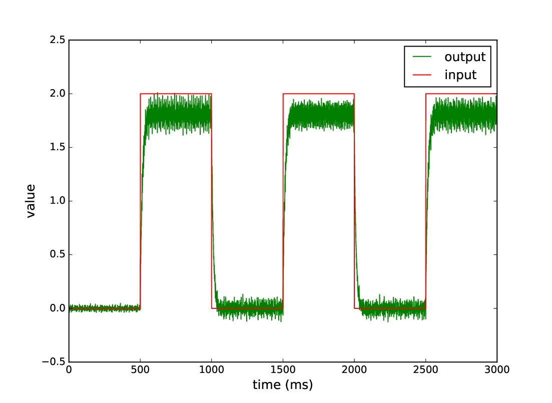
The communication channel is simulated on the 8 PEs of the test chip and the dynamic power (i.e. total power subtracted by baseline power) is measured. The test chip runs with 0.5V 200 MHz.
Dividing the dynamic energy of one time step by the number of synaptic events in one time step, we can get the energy per synaptic event as an energy metric which is commonly used in the neuromorphic literature. For the following calculations, we consider two neuron populations each with neurons and dimensions. To calculate the number of synaptic events, two approaches are considered. The first approach is the equivalent synaptic event similar to Braindrop [32]. Here, we consider the number of synaptic events it would be if the connection matrix were not factorized, i.e. connections between two populations, and each spike causing synaptic operations. The second approach is to consider the hardware operations related to the synaptic events, i.e. the MAC operations done by the MAC array and the ADD operations for each neuron that has spiked in a time step. Assuming neurons have spiked in a time step, the number of synaptic operations is . The results of both approaches are shown in Fig. 21. In the first approach, the energy per equivalent synaptic operation is ca. 10 pJ, surpassing Loihi, which has reported 24 pJ per synaptic operation [15]. In the second approach, for higher dimensions, the energy per synaptic operation reaches 20 pJ, approaches and slightly surpasses Loihi.

VI-D Deep Neural Network
! Florian
For benchmarking the 2D cross-correlation and matrix multiplication accelerator we select individual layers from Lenet [33], VGG-16 [34], ResNet-50 [35] and MobileNetV2 [36] and compare the results with a comparable execution with ARMNN[37] on the ARM4F core. For a study of complete DNNs, please refer to the simulation study by [13]. We divide the layers to fit into the 128kByte SRAM per PE and optimize to utilize each MAC cell of the accelerator as much as possible. The data is send into each of the 8 PEs and then processed 100000 times in a loop. For time measurements we use the ARM core SysTick timer. Because of the possibility to control PE clock frequency and supply voltage we sweep over both while reading out shunt voltage of each power lane with a sampling rate of 100ms. Fig. 22 presents the speed up of the chosen layers and Fig. 23 the gained energy efficiency respectively.
- should I write up some meta data ? - As single runs are very short, we measures in the loop for 1 or 2 seconds. Timer measurements are used for throughput calculation - shmoo show TOPS/W on the right bar - shmoo conv if better values
VI-E Results Summary
VII Conclusion
Outlook/Conclusion: paper shows of the range of possible network types that SpiNNaker2 can be used for. Especially hybrid neural networks, i.e. various crossovers between SNNs and DNNs, can benefit from the SpiNNaker2 architecture. Possibilities of combining MACs with spiking neurons: -as shown, for multi-bit synaptic current input to spiking neurons -Dynamically sparse DNNs, i.e. where information is transmitted only on some form of change, not on a frame-by-frame basis. -a learning-to-learn loop where the inner network is a spiking one and the outer network is a DNN optimizing some target function by modifying the inner spiking network -multi-scale modelling, DNNs realize rate-based or mesoscopic networks, interface with spiking networks
go through metrics/results, compare to other hardware
state-of-the-art ML: - Sticker-T [38] achieves 50 TOPs/W 4-bit
Industry overview: [39]
Other architectures to compare: - TrueNorth SNN + eventuell Joule per inference for DNN tasks - Loihi - BrainDrop for equivalent SynOp? - key-word spotting paper, which compares different approaches.
latest BrainScales-2 system has option for analog vector-matrix multiplication and HAGEN-mode HICANN-DLS [42, 43]. - 5-bit input, 6-bit weight, 8-bit neuron activation - 12 mJ per image (conv network) 3 mJ for smaller dense network
- SNN: [44] 4uJ per image. Simple MLP, with latency code. They try spike sparsity by adding a term to the loss function
Interesting comparison of SNN and DNN by UC Waterloo for same network architecture: [45] They actually use a conv operation in the input layer.
References
- [1] C. Mead, “Neuromorphic electronic systems,” Proceedings of the IEEE, vol. 78, no. 10, p. 1629–1636, 1990.
- [2] K. Roy, A. Jaiswal, and P. Panda, “Towards spike-based machine intelligence with neuromorphic computing,” Nature, vol. 575, no. 7784, p. 607–617, Nov 2019. [Online]. Available: https://doi.org/10.1038/s41586-019-1677-2
- [3] C. Mayr, S. Hoeppner, and S. Furber, “Spinnaker 2: A 10 million core processor system for brain simulation and machine learning,” arXiv preprint arXiv:1911.02385, 2019.
- [4] S. B. Furber, F. Galluppi, S. Temple, and L. A. Plana, “The spinnaker project,” Proceedings of the IEEE, vol. 102, no. 5, p. 652–665, 2014.
- [5] R. Carter, J. Mazurier, L. Pirro, J. Sachse, P. Baars, J. Faul, C. Grass, G. Grasshoff, P. Javorka, T. Kammler, A. Preusse, S. Nielsen, T. Heller, J. Schmidt, H. Niebojewski, P. Chou, E. Smith, E. Erben, C. Metze, C. Bao, Y. Andee, I. Aydin, S. Morvan, J. Bernard, E. Bourjot, T. Feudel, D. Harame, R. Nelluri, H. . Thees, L. M-Meskamp, J. Kluth, R. Mulfinger, M. Rashed, R. Taylor, C. Weintraub, J. Hoentschel, M. Vinet, J. Schaeffer, and B. Rice, “22nm fdsoi technology for emerging mobile, internet-of-things, and rf applications,” in 2016 IEEE International Electron Devices Meeting (IEDM), Dec 2016, p. 2.2.1–2.2.4.
- [6] S. Höppner, H. Eisenreich, D. Walter, U. Steeb, A. S. Clifford Dmello, R. Sinkwitz, H. Bauer, A. Oefelein, F. Schraut, J. Schreiter, R. Niebsch, S. Scherzer, U. Hensel, J. Winkler, and M. Orgis, “How to achieve world-leading energy efficiency using 22fdx with adaptive body biasing on an arm cortex-m4 iot soc,” in ESSDERC 2019 - 49th European Solid-State Device Research Conference (ESSDERC), 2019, p. 66–69.
- [7] S. Höppner, Y. Yan, B. Vogginger, A. Dixius, J. Partzsch, F. Neumärker, S. Hartmann, S. Schiefer, S. Scholze, G. Ellguth, L. Cederstroem, M. Eberlein, C. Mayr, S. Temple, L. Plana, J. Garside, S. Davison, D. R. Lester, and S. Furber, “Dynamic voltage and frequency scaling for neuromorphic many-core systems,” in 2017 IEEE International Symposium on Circuits and Systems (ISCAS), May 2017, p. 1–4.
- [8] S. Höppner, B. Vogginger, Y. Yan, A. Dixius, S. Scholze, J. Partzsch, F. Neumärker, S. Hartmann, S. Schiefer, G. Ellguth, L. Cederstroem, L. A. Plana, J. Garside, S. Furber, and C. Mayr, “Dynamic power management for neuromorphic many-core systems,” IEEE Transactions on Circuits and Systems I: Regular Papers, vol. 66, no. 8, p. 2973–2986, 2019. [Online]. Available: https://ieeexplore.ieee.org/document/8701528
- [9] E. Painkras, L. A. Plana, J. Garside, S. Temple, F. Galluppi, C. Patterson, D. R. Lester, A. D. Brown, and S. B. Furber, “Spinnaker: A 1-w 18-core system-on-chip for massively-parallel neural network simulation,” IEEE Journal of Solid-State Circuits, vol. 48, no. 8, p. 1943–1953, Aug 2013.
- [10] J. Partzsch, S. Höppner, M. Eberlein, R. Schüffny, C. Mayr, D. R. Lester, and S. Furber, “A fixed point exponential function accelerator for a neuromorphic many-core system,” in 2017 IEEE International Symposium on Circuits and Systems (ISCAS), May 2017, p. 1–4.
- [11] M. Mikaitis, D. R. Lester, D. Shang, S. Furber, G. Liu, J. Garside, S. Scholze, S. Höppner, and A. Dixius, “Approximate fixed-point elementary function accelerator for the spinnaker-2 neuromorphic chip,” in 2018 IEEE 25th Symposium on Computer Arithmetic (ARITH), 2018, pp. 37–44.
- [12] F. Neumarker, S. Höppner, A. Dixius, and C. Mayr, “True random number generation from bang-bang ADPLL jitter,” in 2016 IEEE Nordic Circuits and Systems Conference (NORCAS), Nov 2016, p. 1–5.
- [13] F. Kelber, B. Wu, B. Vogginger, J. Partzsch, C. Liu, M. Stolba, and C. Mayr, “Mapping deep neural networks on spinnaker2,” in NICE 2020: Neuro-Inspired Computational Elements Workshop, 2020.
- [14] Y. Yan, T. C. Stewart, X. Choo, B. Vogginger, J. Partzsch, S. Hoeppner, F. Kelber, C. Eliasmith, S. Furber, and C. Mayr, “Low-power low-latency keyword spotting and adaptive control with a spinnaker 2 prototype and comparison with loihi,” arXiv e-prints, p. arXiv:2009.08921, Sep. 2020.
- [15] M. Davies, S. N., T. H. Lin, G. Chinya, Y. Cao, S. H. Choday, G. Dimou, P. Joshi, N. Imam, S. Jain, Y. Liao, C. K. Lin, A. Lines, R. Liu, D. Mathaikutty, S. McCoy, A. Paul, J. Tse, G. Venkataramanan, Y. H. Weng, A. Wild, Y. Yang, and H. Wang, “Loihi: A neuromorphic manycore processor with on-chip learning,” IEEE Micro, vol. 38, no. 1, p. 82–99, January 2018.
- [16] S. B. Furber, F. Galluppi, S. Temple, and L. A. Plana, “The SpiNNaker project,” Proceedings of the IEEE, vol. 102, no. 5, p. 652–665, 2014.
- [17] P. A. Merolla, J. V. Arthur, R. Alvarez-Icaza, A. S. Cassidy, J. Sawada, F. Akopyan, B. L. Jackson, N. Imam, C. Guo, Y. Nakamura et al., “A million spiking-neuron integrated circuit with a scalable communication network and interface,” Science, vol. 345, no. 6197, p. 668–673, 2014.
- [18] C. Frenkel, M. Lefebvre, J.-D. Legat, and D. Bol, “A 0.086-mm 9.8-pJ/SOP 64k-synapse 256-neuron online-learning digital spiking neuromorphic processor in 28nm CMOS,” IEEE Transactions on Biomedical Circuits and Systems, vol. 13, p. 145–158, 2019.
- [19] S. Moradi, N. Qiao, F. Stefanini, and G. Indiveri, “A scalable multicore architecture with heterogeneous memory structures for dynamic neuromorphic asynchronous processors (dynaps),” IEEE transactions on biomedical circuits and systems, 2017.
- [20] C. Mayr, J. Partzsch, M. Noack, S. Hänzsche, S. Scholze, S. Höppner, G. Ellguth, and R. Schüffny, “A biological-realtime neuromorphic system in 28 nm CMOS using low-leakage switched capacitor circuits,” IEEE transactions on biomedical circuits and systems, vol. 10, no. 1, p. 243–254, 2016.
- [21] A. R. Voelker, D. Rasmussen, and C. Eliasmith, “A spike in performance: Training hybrid-spiking neural networks with quantized activation functions,” arXiv preprint arXiv:2002.03553, 2020.
- [22] J. Wu, S. Furber, and J. Garside, “A programmable adaptive router for a gals parallel system,” in 2009 15th IEEE Symposium on Asynchronous Circuits and Systems, 2009, p. 23–31.
- [23] J. Wu and S. Furber, “A multicast routing scheme for a universal spiking neural network architecture,” The Computer Journal, vol. 53, no. 3, p. 280–288, 2010.
- [24] Y. Yan, D. Kappel, F. Neumärker, J. Partzsch, B. Vogginger, S. Höppner, S. Furber, W. Maass, R. Legenstein, and C. Mayr, “Efficient reward-based structural plasticity on a spinnaker 2 prototype,” IEEE Transactions on Biomedical Circuits and Systems, vol. 13, no. 3, p. 579–591, 2019.
- [25] Y.-H. Chen, J. S. Emer, and V. Sze, “Using dataflow to optimize energy efficiency of deep neural network accelerators.” IEEE Micro, vol. 37, no. 3, p. 12–21, 2017.
- [26] S. M. A. Zeinolabedin, F. M. Schüffny, R. George, F. Kelber, H. Bauer, S. Scholze, S. Hänzsche, M. Stolba, A. Dixius, G. Ellguth et al., “A 16-channel fully configurable neural soc with 1.52w/ch signal acquisition, 2.79w/ch real-time spike classifier, and 1.79 tops/w deep neural network accelerator in 22 nm fdsoi,” IEEE Transactions on Biomedical Circuits and Systems, vol. 16, no. 1, p. 94–107, 2022.
- [27] S. Höppner, H. Eisenreich, D. Walter, A. Scharfe, A. Oefelein, F. Schraut, J. Schreiter, T. Riedel, H. Bauer, R. Niebsch, S. Scherzer, T. Hocker, S. Scholze, S. Henker, M. Nossmann, U. Hensel, and H. Prengel, “Adaptive body bias aware implementation for ultra-low-voltage designs in 22fdx technology,” IEEE Transactions on Circuits and Systems II: Express Briefs, p. 1–1, 2019.
- [28] F. Schraut, H. Eisenreich, S. Höppner, and C. Mayr, “A fast lock-in ultra low-voltage ADPLL clock generator with adaptive body biasing in 22nm FDSOI technology,” in 2019 IEEE International Symposium on Circuits and Systems (ISCAS), 2019, p. 1–5.
- [29] M. Abeles, “Synfire chains,” Scholarpedia, vol. 4, no. 7, p. 1441, 2009.
- [30] C. Eliasmith and C. H. Anderson, Neural Engineering (Computational Neuroscience Series): Computational, Representation, and Dynamics in Neurobiological Systems. Cambridge, MA, USA: MIT Press, 2002.
- [31] A. Mundy, J. Knight, T. C. Stewart, and S. Furber, “An efficient spinnaker implementation of the neural engineering framework,” in 2015 International Joint Conference on Neural Networks (IJCNN), 2015, p. 1–8.
- [32] A. Neckar, S. Fok, B. V. Benjamin, T. C. Stewart, N. N. Oza, A. R. Voelker, C. Eliasmith, R. Manohar, and K. Boahen, “Braindrop: A mixed-signal neuromorphic architecture with a dynamical systems-based programming model,” Proceedings of the IEEE, vol. 107, no. 1, p. 144–164, 2019.
- [33] Y. Lecun, L. Bottou, Y. Bengio, and P. Haffner, “Gradient-based learning applied to document recognition,” Proceedings of the IEEE, vol. 86, no. 11, pp. 2278–2324, 1998.
- [34] K. Simonyan and A. Zisserman, “Very deep convolutional networks for large-scale image recognition,” arXiv preprint arXiv:1409.1556, 2014.
- [35] K. He, X. Zhang, S. Ren, and J. Sun, “Deep residual learning for image recognition,” in The IEEE Conference on Computer Vision and Pattern Recognition (CVPR), June 2016.
- [36] M. Sandler, A. Howard, M. Zhu, A. Zhmoginov, and L.-C. Chen, “Mobilenetv2: Inverted residuals and linear bottlenecks,” in 2018 IEEE/CVF Conference on Computer Vision and Pattern Recognition, 2018, pp. 4510–4520.
- [37] L. Lai, N. Suda, and V. Chandra, “Cmsis-nn: Efficient neural network kernels for arm cortex-m cpus.” CoRR, vol. abs/1801.06601, 2018. [Online]. Available: http://dblp.uni-trier.de/db/journals/corr/corr1801.html#abs-1801-06601
- [38] J. Yue, R. Liu, W. Sun, Z. Yuan, Z. Wang, Y.-N. Tu, Y.-J. Chen, A. Ren, Y. Wang, M.-F. Chang et al., “7.5 a 65nm 0.39-to-140.3 tops/w 1-to-12b unified neural network processor using block-circulant-enabled transpose-domain acceleration with 8.1 higher tops/mm 2 and 6t hbst-tram-based 2d data-reuse architecture,” in 2019 IEEE International Solid-State Circuits Conference-(ISSCC). IEEE, 2019, pp. 138–140.
- [39] U. Rueckert, “Digital neural network accelerators,” in NANO-CHIPS 2030, B. Murmann and B. Hoefflinger, Eds. Springer, 2020, pp. 181–202. [Online]. Available: https://doi.org/10.1007/978-3-030-18338-7_12
- [40] J. Pei, L. Deng, S. Song, M. Zhao, Y. Zhang, S. Wu, G. Wang, Z. Zou, Z. Wu, W. He, F. Chen, N. Deng, S. Wu, Y. Wang, Y. Wu, Z. Yang, C. Ma, G. Li, W. Han, H. Li, H. Wu, R. Zhao, Y. Xie, and L. Shi, “Towards artificial general intelligence with hybrid tianjic chip architecture,” Nature, vol. 572, no. 7767, pp. 106–111, 2019, cited By 52.
- [41] L. Deng, G. Wang, G. Li, S. Li, L. Liang, M. Zhu, Y. Wu, Z. Yang, Z. Zou, J. Pei, Z. Wu, X. Hu, Y. Ding, W. He, Y. Xie, and L. Shi, “Tianjic: A unified and scalable chip bridging spike-based and continuous neural computation,” IEEE Journal of Solid-State Circuits, vol. 55, no. 8, pp. 2228–2246, 2020.
- [42] J. Schemmel, S. Billaudelle, P. Dauer, and J. Weis, “Accelerated analog neuromorphic computing,” 2020.
- [43] J. Weis, P. Spilger, S. Billaudelle, Y. Stradmann, A. Emmel, E. Müller, O. Breitwieser, A. Grübl, J. Ilmberger, V. Karasenko, M. Kleider, C. Mauch, K. Schreiber, and J. Schemmel, “Inference with artificial neural networks on analog neuromorphic hardware,” 2020.
- [44] B. Cramer, S. Billaudelle, S. Kanya, A. Leibfried, A. Grübl, V. Karasenko, C. Pehle, K. Schreiber, Y. Stradmann, J. Weis, J. Schemmel, and F. Zenke, “Training spiking multi-layer networks with surrogate gradients on an analog neuromorphic substrate,” 2020.
- [45] P. Blouw and C. Eliasmith, “Event-driven signal processing with neuromorphic computing systems,” in ICASSP 2020-2020 IEEE International Conference on Acoustics, Speech and Signal Processing (ICASSP). IEEE, 2020, pp. 8534–8538.
- [46] C. Ostrau, J. Homburg, C. Klarhorst, M. Thies, and U. Rückert, “Benchmarking deep spiking neural networks on neuromorphic hardware,” in Artificial Neural Networks and Machine Learning – ICANN 2020, I. Farkaš, P. Masulli, and S. Wermter, Eds. Cham: Springer International Publishing, 2020, pp. 610–621.
- [47] C. Ostrau, C. Klarhorst, M. Thies, and U. Rückert, “Comparing neuromorphic systems by solving sudoku problems,” in 2019 International Conference on High Performance Computing Simulation (HPCS), 2019, pp. 521–527.
- [48] M. Davies, “Benchmarks for progress in neuromorphic computing,” Nature Machine Intelligence, vol. 1, no. 9, pp. 386–388, 2019.
- [49] J. C. Knight and T. Nowotny, “Gpus outperform current hpc and neuromorphic solutions in terms of speed and energy when simulating a highly-connected cortical model,” Frontiers in neuroscience, vol. 12, p. 941, 2018.
![[Uncaptioned image]](2103.08392v2/photo_hoeppner.png) |
Sebastian Höppner is a Research Group Leader and Lecturer with the Chair of Highly-Parallel VLSI-Systems and Neuromorphic Circuits. He received the Dipl.-Ing. (M.Sc.) in Electrical Engineering in 2008 and his Ph.D. in 2013 (received Barkhausen Award), both Technische Universität Dresden, Germany. His research interests include circuits for low-power systems-on-chip in advanced technology nodes, with special focus on clocking, data transmission and power management. He has experience in designing full-custom circuits for multi-processor systems-on-chip (MPSoCs), like ADPLLs, register files and high-speed on-chip and off-chip links, in academic and industrial research projects. He has been managing the full-custom circuit design and SoC integration for more than 12 MPSoC chips in 65nm, 28nm and 22nm CMOS technology. Currently he leads the chip design of the SpiNNaker2 neuromorphic computing system within the Human Brain Project(HBP). He is author or co-author of more than 56 publications and 10 patents (5 issued, 5 pending) in the above fields. |
![[Uncaptioned image]](2103.08392v2/photo_yan.png) |
Yexin Yan received the Dipl.-Ing. (M.Sc.) in Electrical Engineering from Technische Universität Dresden, Germany, in 2016. He is currently pursuing the Ph.D. at the Chair of Highly-Parallel VLSI-Systems and Neuromorphic Circuits at Technische Universität Dresden. His research interests include hardware-software co-design for low power neuromorphic applications. |
![[Uncaptioned image]](2103.08392v2/photo_vogginger.png) |
Bernhard Vogginger received the diploma in physics from the University of Heidelberg, Heidelberg, Germany, in 2010. Currently, he is a research associate at the Chair of Highly-Parallel VLSI-Systems and Neuromorphic Circuits at Technische Universität Dresden, Germany, where he is pursuing a PhD under the supervision of Prof. Christian Mayr. His research interests include neuromorphic engineering, neural computation and deep learning. |
![[Uncaptioned image]](2103.08392v2/photo_dixius.png) |
Chen Liu received the Dipl.-Ing. (M.Sc.) in |
![[Uncaptioned image]](2103.08392v2/bio_photos/photo_stolba.jpg) |
Marco Stolba is a PhD student with the Chair of Highly-Parallel VLSI-Systems and Neuromorphic Circuits. He received his MSc degree in Nanoelectronic Systems in 2016 from TU Dresden. His research interests include network on chip (NoC), MPSoC architectures, digital design and verification. |
![[Uncaptioned image]](2103.08392v2/bio_photos/photo_kelber.jpg) |
Florian Kelber is a PhD student at the Chair for Highly-Parallel VLSI-Systems and Neuromorphic circuits at Technische Universität Dresden, Germany. He received the Dipl.-Ing. (M.Sc.) in Information Systems Engineering at degree from Technische Universität Dresden, Germany. His research focus is the design of digital low-power accelerators to mitigate bottlenecks in multi-processor system-on-chip systems and mapping of load-balanced high level algorithms on highly parallel architectures. |
|
Andreas Dixius received the Dipl.-Ing. (M.Sc.) in Information Systems Engineering at Technische Universität Dresden, Germany in 2014. Since 2014 he has been a research assistant at the Chair of Highly-Parallel VLSI-Systems and Neuromorphic Circuits, Technische Universität Dresden, Germany. His research interests include on-chip timing-detection. |
![[Uncaptioned image]](2103.08392v2/photo_scholze.png) |
Stefan Scholze received the Dipl.-Ing. (M.Sc.) in Information Systems Engineering from Technische Universität Dresden, Germany in 2007. Since 2007, he has been a research assistant at the Chair of Highly-Parallel VLSI-Systems and Neuromorphic Circuits, Technische Universität Dresden, Germany. His research interests include design and implementation of low-latency communication channels and systems. |
![[Uncaptioned image]](2103.08392v2/photo_partzsch.png) |
Johannes Partzsch obtained his M.Sc. in Electrical Engineering in 2007 and his PhD in 2014, both from Technische Universität Dresden. He is currently a Research Group Leader at the Chair of Highly-Parallel VLSI-Systems and Neuromorphic Circuits, Technische Universität Dresden, Germany. His research interests include neuromorphic systems design, topological analysis of neural networks and technical application of bio-inspired systems. He is author or co-author of more than 45 publications. |
![[Uncaptioned image]](2103.08392v2/photo_neumaerker.png) |
Felix Neumärker received the Dipl.-Ing. (M.Sc.) in Electrical Engineering from Technische Universität Dresden, Germany, in 2015. He is currently working as research associate with the Chair of Highly-Parallel VLSI-Systems and Neuromorphic Circuits at Technische Universität Dresden. His research interests include software and circuit design and for MPSoCs with special focus on neuromorphic computing. |
![[Uncaptioned image]](2103.08392v2/photo_hartmann.png) |
Stephan Hartmann received the Dipl.-Ing. (M.Sc.) in Electrical Engineering from Technische Universität Dresden, Germany, in 2007. He is currently working as research associate with the Chair of Highly-Parallel VLSI-Systems and Neuromorphic Circuits at Technische Universität Dresden. His research interests include circuit design with special focus on FPGA. |
![[Uncaptioned image]](2103.08392v2/photo_schiefer.png) |
Stefan Schiefer received the Dipl.-Ing. (M.Sc.) in Electrical Engineering from Technische Universität Dresden, Germany in 2008. He is currently working as research associate with the Chair of Highly-Parallel VLSI-Systems and Neuromorphic Circuits at Technische Universität Dresden. His research interests include full system signal and power integrity as well as regulator behavioural modelling including non-linearities. |
![[Uncaptioned image]](2103.08392v2/photo_ellguth.png) |
Georg Ellguth received the Dipl.-Ing. (M.Sc.) in Electrical Engineering from Technische Universität Dresden, Germany in 2004. Since 2004, he has been a research assistant with the Chair of Highly-Parallel VLSI-Systems and Neuromorphic Circuits at Technische Universität Dresden. His research interests include low-power implementation techniques in multi-processor system-on-chip. |
![[Uncaptioned image]](2103.08392v2/photo_plana.png) |
Luis A Plana (M’97-SM’07) received the Ingeniero Electrónico (Cum Laude) degree from Universidad Simón Bolívar, Venezuela, and the PhD degree in computer science from Columbia University, USA. He was with Universidad Politécnica, Venezuela, for over 20 years, where he was Professor of Electronic Engineering. Currently, he is a Research Fellow in the School of Computer Science, University of Manchester, UK. |
|
Mantas Mikaitis received the Dipl.-Ing. (M.Sc.) in |
![[Uncaptioned image]](2103.08392v2/photo_garside.png) |
Jim Garside received the Ph.D. degree in computer science from The University of Manchester, Manchester, U.K., in 1987, for work in signal processing architecture. Post-doctoral work on parallel processing systems based on Inmos Transputers was followed by a spell in industry writing air traffic control software. Returning to academia gave an opportunity for integrated circuit design work, dominated by design and construction work on asynchronous microprocessors in the 1990s. He has been involved with dynamic hardware compilation, GALS interconnection, and the development of the hardware and software of the SpiNNaker neural network simulator. |
![[Uncaptioned image]](2103.08392v2/photo_furber.png) |
Steve Furber CBE FRS FREng is ICL Professor of Computer Engineering in the School of Computer Science at the University of Manchester, UK. After completing a BA in mathematics and a PhD in aerodynamics at the University of Cambridge, UK, he spent the 1980s at Acorn Computers, where he was a principal designer of the BBC Microcomputer and the ARM 32-bit RISC microprocessor. Over 120 billion variants of the ARM processor have since been manufactured, powering much of the world’s mobile and embedded computing. He moved to the ICL Chair at Manchester in 1990 where he leads research into asynchronous and low-power systems and, more recently, neural systems engineering, where the SpiNNaker project is delivering a computer incorporating a million ARM processors optimised for brain modelling applications. |
![[Uncaptioned image]](2103.08392v2/photo_mayr.png) |
Christian Mayr is a Professor of Electrical Engineering at TU Dresden. He received the Dipl.-Ing. (M.Sc.) in Electrical Engineering in 2003, his PhD in 2008 and Habilitation in 2012, all three from Technische Universität Dresden, Germany. From 2003 to 2013, he has been with Technische Universität Dresden, with a secondment to Infineon (2004-2006). From 2013 to 2015, he did a Postdoc at the Institute of Neuroinformatics, University of Zurich and ETH Zurich, Switzerland. Since 2015, he is head of the Chair of Highly-Parallel VLSI-Systems and Neuromorphic Circuits at Technische Universität Dresden. His research interests include bio-inspired circuits, brain-machine interfaces, AD converters and general mixed-signal VLSI-design. He is author/co-author of over 80 publications and holds 4 patents. He has acted as editor/reviewer for various IEEE and Elsevier journals. His work has received several awards. |