A Tb/s Indoor MIMO Optical Wireless Backhaul System Using VCSEL Arrays
Abstract
In this paper, the design of a multiple-input multiple-output (MIMO) optical wireless communication (OWC) link based on vertical cavity surface emitting laser (VCSEL) arrays is systematically carried out with the aim to support data rates in excess of Tb/s for the backhaul of sixth generation (6G) indoor wireless networks. The proposed design combines direct current optical orthogonal frequency division multiplexing (DCO-OFDM) and a spatial multiplexing MIMO architecture. For such an ultra-high-speed line-of-sight (LOS) OWC link with low divergence laser beams, maintaining alignment is of high importance. In this paper, two types of misalignment error between the transmitter and receiver are distinguished, namely, radial displacement error and orientation angle error, and they are thoroughly modeled in a unified analytical framework assuming Gaussian laser beams, resulting in a generalized misalignment model (GMM). The derived GMM is then extended to MIMO arrays and the performance of the MIMO-OFDM OWC system is analyzed in terms of the aggregate data rate. Novel insights are provided into the system performance based on computer simulations by studying various influential factors such as beam waist, array configuration and different misalignment errors, which can be used as guidelines for designing short range Tb/s MIMO OWC systems.
Index Terms:
Indoor optical wireless communication (OWC), multiple-input multiple-output orthogonal frequency division multiplexing (MIMO-OFDM), vertical cavity surface emitting laser (VCSEL) array, Terabit/s backhaul, generalized misalignment model (GMM).- 2D
- Two Dimensional
- 3D
- Three Dimensional
- 5G
- Fifth Generation
- 6G
- Sixth Generation
- AP
- Access Point
- AEL
- Allowable Exposure Limit
- AF
- Amplify-and-Forward
- ACO-OFDM
- Asymmetrically Clipped Optical OFDM
- AOA
- Angle-Of-Arrival
- APC
- Adaptive Power Control
- AR
- Augmented Reality
- ARPC
- Average Rate Power Control
- ASE
- Area Spectral Efficiency
- ASPC
- Average SINR Power Control
- AWGN
- Additive White Gaussian Noise
- AWGR
- Arrayed Waveguide Grating Router
- BBO
- Backhaul Bottleneck Occurrence
- BER
- Bit Error Ratio
- BPSK
- Binary Phase Shift Keying
- BS
- Base Station
- CBS
- Cell-based Bandwidth Scheduling
- CCDF
- Complementary Cumulative Distribution Function
- CCI
- Co-Channel Interference
- CDF
- Cumulative Distribution Function
- CFFR
- Cooperative FFR
- CLT
- Central Limit Theorem
- CoMP
- Coordinated Multi-Point
- CP
- Cyclic Prefix
- CSI
- Channel State Information
- CPC
- Compound Parabolic Concentrator
- DAS
- Distributed Antenna System
- DSL
- Digital Subscriber Line
- DC
- Direct Current
- DCO-OFDM
- Direct Current-biased Optical Orthogonal Frequency Division Multiplexing
- DDO-OFDM
- Direct Detection Optical OFDM
- DF
- Decode-and-Forward
- DMT
- Discrete Multitone
- DSP
- Digital Signal Processing
- DWDM
- Dense Wavelength Division Multiplexing
- EMI
- Electromagnetic Interference
- eU-OFDM
- Enhanced Unipolar OFDM
- FDE
- Frequency Domain Equalization
- FEC
- Forward Error Correction
- FF
- Fill Factor
- FFR
- Fractional Frequency Reuse
- FFT
- Fast Fourier Transform
- FOV
- Field Of View
- FPC
- Fixed Power Control
- FR
- Full Reuse
- FRF
- Frequency Reuse Factor
- FR-VL
- Full Reuse Visible Light
- FSO
- Free Space Optical
- FTTB
- Fiber-To-The-Building
- FTTH
- Fiber-To-The-Home
- FTTP
- Fiber-To-The-Premises
- GMM
- Generalized Misalignment Model
- IB-VL
- In-Band Visible Light
- ICI
- Inter-Cell Interference
- IM-DD
- Intensity Modulation and Direct Detection
- i.i.d.
- Independent and Identically Distributed
- IFFT
- Inverse Fast Fourier Transform
- IoT
- Internet of Things
- IR
- Infrared
- ISI
- Inter-Symbol Interference
- JTDF
- Joint Transmission with Decode-and-Forward
- LAN
- Local Area Network
- LED
- Light Emitting Diode
- LiFi
- Light Fidelity
- LOS
- Line-Of-Sight
- LPF
- Low Pass Filter
- LSSB
- Lower Single-Side Band
- LTE
- Long-Term Evolution
- MAC
- Medium Access Control
- MC
- Multi-Carrier
- MIMO
- Multiple-Input Multiple-Output
- MHP
- Most Hazardous Position
- MPE
- Maximum Permissible Exposure
- MSE
- Mean Square Error
- MSPC
- Maximum SINR Power Control
- MMSE
- Minimum Mean Square Error
- mmWave
- Millimeter Wave
- NPC
- No Power Control
- LAN
- Local Area Network
- NLOS
- Non-Line-Of-Sight
- NMSE
- Normalized Mean Square Error
- NODF
- Non-Orthogonal Decode-and-Forward
- OFDM
- Orthogonal Frequency Division Multiplexing
- OFDMA
- Orthogonal Frequency Division Multiple Access
- OOK
- On-Off Keying
- OWC
- Optical Wireless Communication
- PAM
- Pulse Amplitude Modulation
- PAPR
- Peak-to-Average Power Ratio
- PD
- Photodetector
- Probability Density Function
- PE
- Power Efficiency
- PHY
- Physical Layer
- PLC
- Power Line Communication
- PMF
- Probability Mass Function
- PoE
- Power-over-Ethernet
- P-OFDM
- Polar OFDM
- PON
- Passive Optical Network
- PPP
- Poisson Point Process
- PSD
- Power Spectral Density
- PTP
- Point-To-Point
- PTMP
- Point-To-Multi-Point
- QAM
- Quadrature Amplitude Modulation
- QoS
- Quality of Service
- QPSK
- Quadrature Phase Shift Keying
- RF
- Radio Frequency
- RGB
- Red-Green-Blue
- RHS
- Right Hand Side
- RIN
- Relative Intensity Noise
- RMS
- Root Mean Square
- RoF
- Radio-over-Fiber
- RTP
- Relative Total Power
- SC
- Single Carrier
- SE
- Spectral Efficiency
- SEE-OFDM
- Spectral and Energy Efficient OFDM
- SINR
- Signal-to-Interference-plus-Noise Ratio
- SISO
- Single Input Single Output
- SM
- Spatial Multiplexing
- SMF
- Single Mode Fiber
- SNR
- Signal-to-Noise Ratio
- SSB-OFDM
- Single-Side Band OFDM
- SVD
- Singular Value Decomposition
- TEM
- Transverse Electromagnetic Mode
- TIA
- Transimpedance Amplifier
- UB
- Unlimited Backhaul
- UBS
- User-based Bandwidth Scheduling
- UE
- User Equipment
- UHD
- Ultra-High-Definition
- USSB
- Upper Single-Side Band
- VCSEL
- Vertical Cavity Surface Emitting Laser
- VPPM
- Variable Pulse Position Modulation
- VL
- Visible Light
- VLC
- Visible Light Communication
- VR
- Virtual Reality
- WDM
- Wavelength Division Multiplexing
- WiFi
- Wireless Fidelity
- WLAN
- Wireless Local Area Network
- WOC
- Wireless Optical Communication
I Introduction
The proliferation of Internet-enabled premium services such as 4K and 8K UHD (UHD) video streaming, immersion into VR (VR) or AR (AR) with 3D (3D) stereoscopic vision, holographic telepresence and multi-access edge computing will extremely push wireless connectivity limits in years to come [2]. These technologies will require an unprecedented system capacity above Tb/s for real-time operation, which is one of the key performance indicators of the future 6G (6G) wireless systems [3].
The achievability of ultra-high transmission rates of Tb/s has been addressed in the literature for both wired and wireless systems [4, 5, 6]. Targeting DSL (DSL) applications, in [4], Shrestha et al. have used a two-wire copper cable as a multi-mode waveguide for MIMO (MIMO) transmission and experimentally measured the received power for signals with GHz bandwidth. They have predicted that aggregate data rates of several Tb/s over a twisted wire pair are feasible at short distances of m by using DMT (DMT) modulation and vector coding. In [5], the authors have reported successful implementation of a Tb/s super channel over a km optical SMF (SMF) link based on QAM (QAM) with probabilistic constellation shaping. In [6], Petrov et al. have elaborated on a roadmap to actualize last meter indoor broadband wireless access in the terahertz band, i.e. – THz, in order to enable Tb/s connectivity between the wired backbone infrastructure and personal wireless devices.
The feasibility of Tb/s data rates has been actively studied for outdoor point-to-point FSO (FSO) communications [7, 8, 9]. In [7], Ciaramella et al. have presented experimental results for a terrestrial FSO link achieving a net data rate of Tb/s over a distance of m using WDM (WDM) channels centered at nm and direct detection. In [8], Parca et al. have demonstrated a transmission rate of Tb/s over a hybrid fiber and FSO system with a total distance of m based on polarization multiplexing, WDM channels and coherent detection. In [9], Poliak et al. have set up a field experiment emulating the uplink FSO transmission in ground-to-geostationary satellite communications under adverse atmospheric turbulence conditions, corroborating a throughput of Tb/s over km with the aid of WDM OOK (OOK) channels and active beam tracking at the receiver.
Beam-steered IR (IR) light communication is an OWC (OWC) technology primarily tailored to provide multi-Gb/s data rates per user by directing narrow IR laser beams at mobile devices. In [10], Koonen et al. have proposed a wavelength-controlled beam steering technique by using a 2D (2D) high port-count AWGR (AWGR) array and a lens. The authors have demonstrated Gb/s - PAM (PAM) transmission with m reach based on an -ports AWGR, anticipating a total throughput of about Tb/s when all the beams are in use. In [11], Sun et al. have proposed an alternative optical design employing a fiber port array and a transceiver lens to provide full beam coverage within the desired area without beam steering. The authors have shown that this system supports Gb/s single-user transmission rates and over Tb/s multi-user sum rates.
Indoor laser-based optical wireless access networks can generate aggregate data rates beyond Tb/s [12]. Such ultra-high-speed indoor access networks impose a substantial overhead on the backhaul capacity, and a cost-effective backhaul solution is a major challenge. In this paper, a high-capacity wireless backhaul system is designed based on laser-based OWC to support aggregate data rates of at least Tb/s for backhaul connectivity in next generation Tb/s indoor networks. While FSO systems suffer from outdoor channel impairments such as weather-dependent absorption loss and atmospheric turbulence, short range laser-based OWC under stable and acclimatized conditions of indoor environments potentially enhances the signal quality. This way, the need for bulky FSO transceivers equipped with expensive subsystems to counteract outdoor effects is eliminated. Moreover, the aforementioned FSO systems use DWDM (DWDM) to deliver Tb/s data rates, which significantly increases the cost and complexity of the front-end system.
Different from WDM FSO systems, in this paper, a single wavelength is used to achieve a data rate of Tb/s by means of VCSEL. The choice of VCSEL for the optical wireless system design is motivated by the fact that, among various types of laser diodes, VCSEL are one of the strongest contenders to fulfil this role due to several important features of them, including [13, 14]: 1) a high modulation bandwidth of GHz; 2) a high power conversion efficiency of ; 3) cost-efficient fabrication by virtue of their compatibility with large scale integration processes; 4) possibility for multiple devices to be densely packed and precisely arranged as 2D arrays. These attributes make VCSEL appealing to many applications such as optical networks, highly parallel optical interconnects and laser printers, to name a few [15]. Single mode VCSEL, which are the focus of this paper, generate an output optical field in the fundamental TEM (TEM) (i.e. mode), resulting in a Gaussian profile on the transverse plane, in that the optical power is maximum at the center of the beam spot and it decays exponentially with the squared radial distance from the center [16].
For LOS (LOS) OWC links, accurate alignment between the transmitter and receiver is a determining factor of the system performance and reliability. In principle, two types of misalignment may occur in the link: radial displacement between the transmitter and receiver, and orientation angle error at the transmitter or receiver side. Modeling of the Gaussian beam misalignment has been addressed in the context of terrestrial FSO systems such as the works of Farid and Hranilovic, for SISO (SISO) [17] and MIMO [18] links. The FSO transceiver equipment is commonly installed on the rooftops of high-rise buildings and hence random building sways due to wind loads and thermal expansions cause a pointing error in the transmitter orientation angle with independent and identical random components in elevation and horizontal directions [19]. The works in [17, 18, 19] implicitly base their modeling methodology on the assumption of treating the effect of this angle deviation at the transmitter (with a typical value of mrad) as a radial displacement of the beam spot position at the receiver (typically located at km distance from the transmitter). By contrast, in [20], Huang and Safari, through applying a small angle approximation, have modeled the receiver-induced AOA (AOA) misalignment again as a radial displacement of the optical field pattern on the PD (PD) plane. In [21, 22], Poliak et al. have presented a link budget model for FSO systems in an effort to incorporate misalignment losses for Gaussian beams individually, including lateral displacement, tilt of the transmitter and tilt of the receiver. Nonetheless, the effect of these tilt angles has been simplified by a lateral displacement. In [23], Azzolin et al. have proposed an exact analytical solution in terms of the Marcum Q-function for the geometric and misalignment loss in SISO FSO links in the presence of only radial displacement of the Gaussian beam spot at the circular aperture of the receiver.
Although the problem of misalignment constitutes an important practical challenge for designing Tb/s indoor optical wireless links as a key enabler for ultra-high-speed networks of the future, it has not been widely studied yet. For short range indoor OWC systems with compact PD, to minimize the geometric loss, the beam spot size is required to be relatively small, comparable to the size of a PD, in which case angular misalignment can significantly influence the link performance, independent of the radial displacement error. In a previous work [1], the authors have presented preliminary results to study the effect of only displacement error on the performance of indoor Tb/s MIMO OWC. However, such high performance indoor OWC links are essentially prone to any type of misalignment errors. To the best of the authors’ knowledge, there is a lack of a comprehensive and analytically tractable model of the link misalignment for laser-based OWC systems inclusive of orientation angle errors at the transmitter and receiver sides as well as the radial displacement error. This paper puts forward the modeling and design of a spatial multiplexing MIMO OWC system based on DCO-OFDM (DCO-OFDM) and VCSEL arrays to unlock Tb/s data rates with single mode VCSEL. The contributions of this paper are concisely given as follows:
- •
An in-depth analytical modeling of the misalignment for SISO optical wireless channels with Gaussian beams is presented. Thereupon, a GMM (GMM) is derived where radial displacement and orientation angle errors at both the transmitter and receiver sides are all taken into consideration in a unified manner. This model is verified by computer simulations using a commercial optical design software, Zemax OpticStudio.
- •
- •
The spatial multiplexing MIMO-OFDM transceiver under consideration is elucidated and the received SINR (SINR) and aggregate data rate are analyzed. It is shown that treating an angular pointing error of the transmitter as a radial displacement is a special case of the GMM and a tight analytical approximation of the MIMO channel DC (DC) gains is derived for this case.
The remainder of the paper is organized as follows. In Section II, the SISO channel model for a perfectly aligned VCSEL-based OWC system is described. In Section III, the detailed analytical modeling framework for the generalized misalignment of the SISO channel is established. In Section IV, the design and analysis of the MIMO-OFDM OWC system using VCSEL and PD arrays is presented, including the incorporation of the GMM in the MIMO channel model. In Section V, numerical results are provided. In Section VI, concluding remarks are drawn and a number of possible directions are suggested for the future research.

II VCSEL-based Optical Wireless Channel
A MIMO OWC system can be realized by means of an array of VCSEL. Fig. 1 illustrates a MIMO system configuration, comprising a VCSEL array and a PD array, which are perfectly aligned to each other. There is a directed LOS link from every VCSEL to its corresponding PD as represented by an exclusive color. This section deals with the channel model for a VCSEL-based SISO optical wireless link as a building block for the MIMO system.
II-A Gaussian Beam Propagation
The wavefront of the Gaussian beam is initially planar at the beam waist and then expanding in the direction of propagation. The wavefront radius of curvature at distance from the transmitter is characterized by [16]:
| (1) |
where is the waist radius; and is the laser wavelength. Also, the radius of the beam spot, which is measured at the normalized intensity contour on the transverse plane, takes the following form [16]:
| (2) |
where is the Rayleigh range. It is defined as the distance at which the beam radius is extended by a factor of , i.e. . In this case, the beam spot has an area twice that of the beam waist. The Rayleigh range is related to and via [16]:
| (3) |
From (2), for approaches the asymptotic value:
| (4) |
thus varying linearly with . Therefore, the circular beam spot in far field is the base of a cone whose vertex lies at the center of the beam waist with a divergence half-angle:
| (5) |
The spatial distribution of a Gaussian beam along its propagation axis is described by the intensity profile on the transverse plane. By using Cartesian coordinates, the intensity distribution at distance from the transmitter at the point is given by [16]:
| (6) |
where is the transmitted optical power; and is the Euclidean distance of the point from the center of the beam spot.
II-B Channel DC Gain
As observed from (6), the fundamental property of the Gaussian beam propagation is that the intensity distribution is given on the transverse plane as a circularly symmetric function centered about the beam axis. For a general link configuration, the transmitter and receiver are oriented toward arbitrary directions in the 3D space with and denoting their normal vectors, respectively. In this case, the received optical power is obtained by integrating (6) over the effective area of the PD [24]. To this end, the PD area is projected onto the transverse plane by using the cosine of the normal vector of the PD plane with respect to the beam propagation axis, which is equal to . The DC gain of an IM-DD (IM-DD) channel is defined as the ratio of the average optical power of the received signal to that of the transmitted signal. Therefore, the DC gain of the channel is calculated as follows:
| (7) |
where denotes the PD area; and the factor accounts for Lambert’s cosine law. Throughout the paper, a circular PD of radius is assumed for which .

Fig. 2 illustrates a SISO OWC system in a directed LOS configuration with perfect alignment. In this case, the beam waist plane is parallel to the PD plane so that and the center of the beam spot is exactly located at the center of the PD. Hence, in (6) is equal to on the PD plane. From (7), for a link distance of , the DC gain of the channel becomes:
| (8) |
where .
III Generalized Misalignment Modeling
This section establishes a mathematical framework for the analytical modeling of misalignment errors for the SISO optical wireless channel discussed in Section II. In the following, two cases of displacement error and orientation angle error are presented.

III-A Displacement Error
A displacement error between the transmitter and receiver causes the center of the beam spot at the PD plane to deviate radially, relative to the center of the PD, which is equivalent to the radial displacement in [17]. In this case, . The magnitude of the error is represented by , where and correspond to the error components along the and axes, as shown in Fig. 3. It can be observed that the intensity value depends on the axial distance between the beam waist and the PD plane where , and the Euclidean distance from the center of the beam spot to the coordinates . It follows that:
| (9) |
Substituting (9) in (7), the DC gain of the channel turns into:
| (10) |


III-B Orientation Angle Error
An orientation error occurs when the transmitter or receiver has a non-zero tilt angle with respect to the alignment axis. Orientation angles of the transmitter and receiver, denoted by and , respectively, entail arbitrary and independent directions in the 3D space. Note that the transmitter and receiver orientation errors are jointly modeled, though they are separately depicted in Fig. 4 to avoid intricate geometry. Furthermore, the angles and are decomposed into azimuth and elevation components in the 3D space using the rotation convention shown in Fig. 4.
The aim is to determine the intensity at a given point on the PD surface based on (6). To elaborate, according to Fig. 4, consider the family of concentric, closed disks perpendicular to the beam axis, with their centers lying on the beam axis. Among them, the one with a circumference intersecting the point on the PD plane is the basis for analysis. This particular disk is referred to as principal disk hereinafter, which is drawn as a yellow disk in Fig. 4. The variables to be characterized are the axial distance between the beam waist and the center of the principal disk and the Euclidean distance of the point to the beam axis, i.e. the radius of the principal disk.
The PD’s coordinate system is rotated with respect to the reference coordinate system as shown in Fig. . Based on Euler angles with clockwise rotations, the system is transformed into the system by rotating first about the axis through an angle , then about the axis through an angle , using the following rotation matrices:
| (11a) | ||||
| (11b) | ||||
for and . The desired point is given in the system. The projected coordinates of this point in the system is obtained as:
| (12) |
The axial distance consists of two segments including the projection of onto the beam axis and the additive length :
| (13) |
From Fig. , there are two parallel planes indicated by and so that the additive length can be found as the distance between and , which is subsequently derived in (16). These planes are perpendicular to the beam axis such that passes through the point in the system and crosses the origin. The normal vector of both planes is:
| (14) |
where , and represent unit vectors for , and axes, respectively. Let to simplify notation, where . It follows that:
| (15a) | ||||
| (15b) | ||||
The additive length in (13) is derived by finding the distance from the origin to , resulting in:
| (16) |
Combining (16) with (12) and (14), and using trigonometric identities, yields:
| (17) |
The squared radius of the principal disk illustrated in Fig. is given by:
| (18) |
where:
| (19) |
Substituting , and from (12) into (19), and simplifying, leads to:
| (20) |
The last piece required to complete the analysis of the channel gain based on (7) is the calculation of the inner product of and . From Fig. , the normal vector to the PD surface is:
| (21) |
By using (14) and (21), the cosine of the planar angle between the surface normal and the beam axis is obtained as follows:
| (22) |
By combining (2), (13), (17), (18) and (20), the DC gain of the channel, denoted by , can be evaluated based on (7) and (22) when using:
| (23) | ||||
| (24) | ||||
III-C Unified Misalignment Model
In order to unify displacement and orientation errors, after the transmitter is rotated, it is shifted to the point in the system. Referring to the parallel planes and in (15), now intersects the point . Therefore, from (16), such that , and . Consequently, the squared radius of the principal disk is determined by using (18) in conjunction with (13) and from (19). Altogether, the generalized channel gain is computed based on (7) and (22) through the use of:
| (25) | ||||
| (26) | ||||


IV MIMO OWC System Using VCSEL Arrays
IV-A Structure of Arrays and MIMO Channel
The array structure shown in Fig. 1 is extended to a square, forming an MIMO OWC system where11 1 The assumption of is only used for convenience of the presentation and it is not a necessary requirement. In fact, for the same array structure shown in Fig. 5, the receiver array can be designed such that as discussed in Section V. . Fig. 5 depicts a VCSEL array and a PD array on the plane. The gap between adjacent elements of the PD array is controlled by , which is referred to as inter-element spacing hereinafter. For those PD that are close to the edges of the array, there is a margin of with respect to the edges. The center-to-center distance for neighboring PD along rows or columns of the array is:
| (27) |
The side length for each array is , leading to array dimensions of .
The MIMO channel is identified by an matrix of DC gains for all transmission paths between the transmitter and receiver arrays:
| (28) |
where the entry corresponds to the link from to . For the array structure shown in Fig. 5, the elements are labeled by using a single index according to their row and column indices. This way, for an array, the VCSEL (resp. PD) situated at the th entry of the matrix for is denoted by (resp. ) where . Let and be the coordinates of the th element of the VCSEL and PD arrays, respectively, in the system, for . Under perfect alignment, , , and . Here, are 2D coordinates of the th element on each array. From Fig. 5, it is straightforward to show that:
| (29a) | ||||
| (29b) | ||||
where and , with denoting the smallest integer that satisfies . In this case, evaluating based on (7) leads to:
| (30) |

IV-B Generalized Misalignment of Arrays
Under the generalized misalignment, the whole transmitter and receiver arrays are affected by both displacement and orientation errors. To characterize the MIMO channel with the generalized misalignment, the entries of the MIMO channel matrix can be derived by applying the procedure described in Section III-C for the SISO channel22 2 In consideration of the receiver optics, a non-imaging optical design based on ideal CPC can be used. Such a receiver structure would not alter the spatial distribution of the beam spots at the receiver array, since an ideal lossless CPC transfers all the optical power collected at the entrance aperture to the exit aperture [24]. Therefore, the analytical framework proposed for the generalized misalignment modeling in Section III would still be valid for computing the optical power incident on each receiver element due to the fact that all the integrations can be equally evaluated over the circular area of the entrance aperture of CPC. The optimal design of non-imaging receivers is, however, beyond the scope of this paper and it is subject to a separate study.. Fig. 6 depicts the MIMO link configuration where the transmitter and receiver arrays are rotated according to their respective orientation angles. Note that Fig. 6 does not include radial displacement for simplicity. The corresponding parameters of the SISO link between and are highlighted in blue, as shown in Fig. 6. Considering the generalized misalignment, the VCSEL array is first rotated by an angle and then its center is radially displaced relative to the center of the receiver array. The coordinates of in the reference coordinate system are:
| (31) |
where and are given by (11) for and . Also, after the receiver array undergoes a rotation by an angle , the coordinates of in the system are:
| (32) |
where and are given by (11) for and . To calculate the channel gain between and , denoted by , using (7), the parameters and are evaluated based on (25) and (26) by substituting the link distance for , and the displacement components and for and , respectively. This exact procedure is referred to as the MIMO GMM for brevity.
IV-C Approximation of the MIMO GMM
The computation of the MIMO GMM as described above entails numerical integrations. In the following, approximate analytical expressions of the MIMO channel gain are derived for two special cases of radial displacement and orientation error at the transmitter. Then, the relation between them for a small angle error is elaborated. The area of a circular PD of radius is approximated by an equivalent square of side length with the same area.
IV-C1 Radial Displacement
In this case, , and . Therefore, , and:
| (33) |
From (7), is then written as:
| (34) |
which can be derived as follows:
| (35) | ||||
where is the error function.
IV-C2 Orientation Error of the Transmitter
For the case of orientation angle error at the transmitter, the use of (31) and (32) leads to , and . After simplifying, the parameters and are obtained as:
| (36) |
| (37) | ||||
Considering that and hold, for sufficiently small values of and , , which gives rise to:
| (38) |
This approximation means the axial distance variation of the slightly tilted beam spot over the PD surface is ignored due to its small size. Hence, (36) is simplified to . Besides, when and are small enough, in the right hand side of (37), the last term is deemed negligible compared to the first two terms from the factor . Consequently, using , the integration in (7) is approximated by:
| (39) | ||||
A closed form solution of (39) is readily derived as follows:
| (40) | ||||
Note that (40) essentially represents (35) for and . This means an orientation angle error of the transmitter array with azimuth and elevation components of and produces an effect equivalent to horizontal and vertical displacements of and , respectively. The approximations in (35) and (40) are verified in Appendix and it is shown that they are highly accurate as long as the beam spot size at the receiver is in the order of or larger than the PD size.

IV-D Spatial Multiplexing MIMO-OFDM
IV-D1 Transceiver Architecture
In this paper, a spatial multiplexing MIMO-OFDM system is used to maximize the transmission rate by sending independent data streams over the MIMO optical wireless channel. To ensure a high spectral efficiency for transmitting each data stream, the standard DCO-OFDM technique along with adaptive QAM is used [25]. In this case, the spatial overlapping between the beam spots of the VCSEL at the PD array causes crosstalk in the MIMO channel. Fig. 7 depicts a simplified block diagram of the MIMO-OFDM transceiver architecture. The SVD (SVD) precoding and decoding stages shown in Fig. 7 can be applied provided the MIMO CSI (CSI) is known at both the transmitter and receiver. First, it is assumed that this is not the case to avoid the overhead associated with the CSI estimation and feedback, and the transceiver system is described without the use of SVD.
At the transmitter, the input binary data streams are individually mapped to a sequence of complex QAM symbols. With a digital realization of the OFDM modulation and demodulation by way of -point IFFT (IFFT) and FFT (FFT), respectively, the resulting sequences are buffered into blocks of size . They are loaded onto the data-carrying subcarriers of the OFDM frames in positive frequencies, where . For baseband OFDM transmission in IM-DD systems, it is necessary for the time domain signal to be real-valued. To this end, for each OFDM frame, the number of symbols is extended to according to a Hermitian symmetry and the DC and Nyquist frequency subcarriers are zero-padded before the IFFT operation. Also, in order to comply with the non-negativity constraint of IM-DD channels, a proper DC level is added in the time domain to obtain a positive signal [25]. Let be the vector of instantaneous optical powers emitted by the VCSEL at time sample for . It is given by:
| (41) |
where is the average electrical power of each OFDM symbol; is the vector of the normalized discrete time OFDM samples; is the DC bias with representing the average optical power per VCSEL; and is an all-ones vector. The finite dynamic range of the VCSEL determines the available peak-to-peak swing for their modulating OFDM signal. The envelope of the unbiased OFDM signal follows a zero mean real Gaussian distribution for [26]. The choice of guarantees that of the signal variations remains undistorted, thereby effectively discarding the clipping noise [27]. Thus, the average power of the OFDM signal assigned to each VCSEL is .
At the receiver array, after filtering out the DC component and perfect sampling, the vector of received photocurrents is obtained. Let be the vector of symbols modulated on the th subcarrier in the frequency domain. After the FFT operation, the received symbols are extracted from the data-carrying subcarriers and then they are demodulated using maximum likelihood detection. The vector of received signals on the th subcarrier for is written in the form:
| (42) |
where is the PD responsivity; is the frequency response of the MIMO channel; and is the AWGN (AWGN) vector. Note that without SVD processing, holds, in which case and . Considering strong LOS components when using laser beams with low divergence, the channel is nearly flat for which , where refers to (28). The th element of the noise vector comprises thermal noise and shot noise of the th branch of the receiver and the RIN (RIN) caused by all the VCSEL which depends on the average received optical power [28]. The total noise variance is given by:
| (43) |
where is the Boltzmann constant; is temperature in Kelvin; is the load resistance; is the single-sided bandwidth of the system; is the noise figure of the TIA (TIA); is the elementary charge; and is defined as the mean square of instantaneous power fluctuations divided by the squared average power of the laser source [28]. Based on (42), the received SINR per subcarrier for the th link is derived as follows:
| (44) |
IV-D2 SVD Processing
When the CSI is available at the transmitter and receiver, the MIMO channel can be transformed into a set of parallel independent subchannels by means of SVD of the channel matrix in the frequency domain. The use of SVD leads to the capacity achieving architecture for spatial multiplexing MIMO systems [29]. The SVD of , with , is , where and are unitary matrices; ∗ denotes conjugate transpose; and is a rectangular diagonal matrix of the ordered singular values, i.e. [29]. Note that as discussed so the subscript can be dropped from the singular values. After SVD decoding at the receiver, the -dimensional vector of received symbols on the th subcarrier for becomes:
| (45) |
where . Note that the statistics of the noise vector is preserved under a unitary transformation. Therefore, the th elements of and have the same variance of . The received SNR (SNR) per subcarrier for the th link is derived as follows:
| (46) |
IV-E Aggregate Rate Analysis
Based on adaptive QAM with a given BER (BER) performance in an AWGN channel, a tight upper bound for the number of bits per symbol transmitted by , for and dB, is given by [30]:
| (47) |
where:
| (48) |
represents the SINR gap due to the required BER. With a symbol rate of for DCO-OFDM, the achievable rate per subcarrier is bit/s. According to data-carrying subcarriers, the transmission rate for is then:
| (49) |
where . Hence, the aggregate data rate of the MIMO-OFDM system is expressed as:
| (50) |
| Parameter | Description | Value |
|---|---|---|
| Link distance | m | |
| Transmit power per VCSEL | mW | |
| Laser wavelength | nm | |
| Effective waist radius | µm | |
| System bandwidth | GHz | |
| Laser noise | dB/Hz | |
| PD radius | mm | |
| PD area | mm2 | |
| PD responsivity | A/W | |
| Inter-element spacing | mm | |
| Load resistance | ||
| TIA noise figure | dB | |
| Target BER |
V Numerical Results and Discussions
The performance of the VCSEL-based MIMO OWC system is evaluated by using computer simulations and the parameters listed in Table I, where the VCSEL and noise parameters are adopted from [15, 31]. Numerical results are presented for the effective radius of the beam waist over the range with the assumption that there is a convex lens next to each bare VCSEL to widen its output beam waist in order to reduce the far field beam divergence. For a link distance of m, the beam spot radius and divergence angle vary from mm and to mm and . An optical power per VCSEL of mW is selected on account of eye safety considerations. A laser source is eye-safe if a fraction of the total power of the Gaussian beam entering the eye aperture at the MHP (MHP) for an exposure time of blink reflex is no greater than the MPE (MPE) multiplied by the pupil area [32], i.e. . For a given wavelength, the MPE value reduces with an increase in the beam waist radius [33], so the most restrictive case is when is at a maximum. The case of µm and nm leads to a subtense angle of mrad. The subtense angle is measured as the plane angle subtended by the apparent source to the observer’s pupil at MHP. For mrad, the laser source is classified as a point source for which and W/m2 [33]. For a circular aperture of diameter mm, mm2, and it follows that mW for each VCSEL. Hence, mW is considered eye-safe.
V-A Perfect Alignment
V-A1 Spatial Distribution of SINR
Fig. 8 illustrates the spatial distribution of the received SINR on the transverse plane at the receiver for a PD array, for µm and µm, representing two cases for the beam spot radius including mm and mm, respectively. For µm with a larger beam spot size at the receiver, as shown in Fig. , the SINR ranges from dB to dB. A dissimilar distribution of the SINR over different regions of the array is caused by significant overlaps between the neighboring beam spots. It can be observed that in the regions close to the edge of the array, when compared to other regions, there are larger areas over which the highest SINR level is experienced, as they are influenced by asymmetric crosstalk effects due to their positions relative to the center of the array. The maximum MIMO interference falls on the central region where a small area is covered with the highest SINR level. However, on the positions of the PD elements as shown by small circles, SINR levels are approximately equal, near the maximum value. As shown in Fig. , when doubling the effective waist radius to µm, the value of is halved and the edge effects are improved, since the beam spot area is quarter of the case where µm. In this case, the SINR is almost evenly distributed on different regions and the SINR of dB is equally achieved at each PD.


V-A2 Rate vs. Beam Waist
Fig. 9 demonstrates the aggregate data rate achieved by the proposed MIMO system under perfect alignment conditions when is varied from µm to µm. For all MIMO realizations under consideration, the aggregate rate monotonically increases for larger values of . At the beginning for µm, the beam spot size at the receiver is very large, i.e. mm. This renders the signal power collected by each PD from direct links very low. Besides, there is substantial crosstalk among the incident beams, which severely degrades the performance. The use of SVD yields the upper bound performance for the MIMO system. When increases, the data rate grows, and so does the gap between the performance of the MIMO system without SVD and the upper bound. The maximum difference between the performance of the two systems occurs at about µm. After this point, by increasing , the aforementioned gap is rapidly reduced and the data rate for the MIMO system without SVD asymptotically approaches that with SVD. The right tail of the curves in Fig. 9 indicates the noise-limited region for µm, whereas µm represents the crosstalk-limited region. Also, , , and systems, respectively, attain Tb/s, Tb/s, Tb/s and Tb/s, for µm. In order to achieve a target data rate of Tb/s, , and systems, respectively, require the beam waist radii of µm, µm and µm. This target is not achievable by a system for µm.


and

and

and

, and

mm and

mm and
V-B GMM Verification
The GMM of the SISO channel developed in Section III is the underlying foundation for the MIMO misalignment modeling presented in Section IV. Therefore, its accuracy needs to be verified with a dependable benchmark. A powerful commercial optical design software by Zemax, known as OpticStudio [34], is used for this purpose. Empirical data is collected by running extensive simulations based on non-sequential ray tracing in OpticStudio. Fig. 10 presents a comparison between the results of the GMM and those computed by using OpticStudio for different values of the beam waist radius. Without loss of generality, results are presented by assuming that the radial displacement error of the receiver relative to the transmitter is solely comprised of its horizontal component and that the orientation angle error at both sides of the link only involves the azimuth component, i.e. for and . Six example scenarios are inspected. The first set of results include (a) horizontal displacement for and , (b) azimuth angle error at the transmitter for and , and (c) azimuth angle error at the receiver for and . The aim of these scenarios is to confirm the GMM accuracy when the link undergoes one type of misalignment at a time. The second set of results represents (d) horizontal displacement for and and , (e) transmitter azimuth angle error for mm and , and (f) receiver azimuth angle error for mm and . These scenarios are intended to showcase the GMM accuracy when a combination of radial displacement and orientation angle errors comes about simultaneously. Note that in scenarios (d), (e) and (f), horizontal displacement increases in the negative direction of the axis on the receiver plane. As observed from Figs. and , the channel gain exhibits a peak, which corresponds to the moment that the beam spot center falls onto the PD. As shown in Fig. 10, the GMM accurately predicts the channel gain results obtained by OpticStudio simulations and there is an excellent match between them in all cases. This corroborates the high reliability of the proposed analytical modeling framework.
V-C Impact of Misalignment
The impact of misalignment is studied for an MIMO system with (i.e. VCSEL array) and µm, as this is the case where the maximum data rate can be achieved, though such very low divergence beams are prone to misalignment errors. To make use of the SVD architecture, three configurations of the PD array with different number of elements as shown in Fig. 11 are examined, where in Configs. I, II and III, respectively. For the PD array structure described in Section IV-A, the FF (FF) can be calculated as . The corresponding FF value for Configs. I, II and III is .
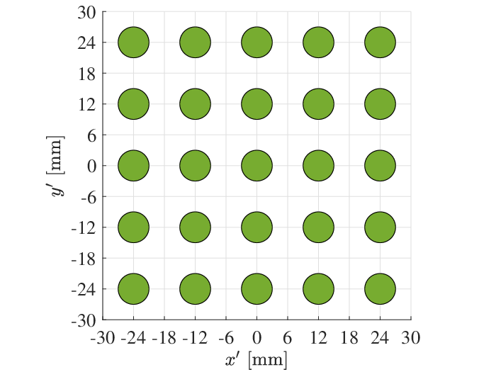
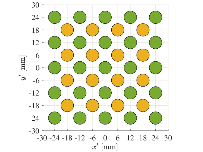
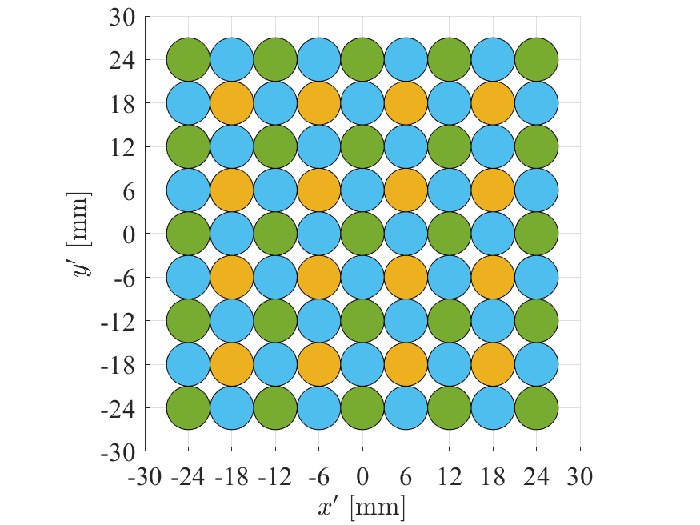
V-C1 Radial Displacement Error
Fig. 12 plots the aggregate data rate of the system with respect to the radial displacement error. ‘Exact’ and ‘Approx.’ labels refer to the exact MIMO GMM procedure from Section IV-B and the approximate formula in (35) used for computing the MIMO channel gains for the case without SVD. The results of the two approaches perfectly match with each other for both scenarios shown in Figs. 12a and 12b. In Fig. , the radial displacement takes place along one of the two lateral dimensions of the PD array relative to the VCSEL array, i.e. horizontally. Note that vertical displacement is similar to this case due to the symmetry in the square lattice of the arrays. It is observed from Fig. that without SVD, the data rate rapidly drops to zero after mm. When using SVD for Config. I, the rate performance exhibits a decaying oscillation with exactly five peaks, each of which corresponds to an event that a given number of columns of the VCSEL array are aligned to those of the PD array. The use of Config. II slightly improves the valleys because of the second lattice of PD placed on the vertices of the first lattice. This keeps the aggregate data rate above Tb/s for mm. By comparison, significant performance improvements are attained with SVD and Config. III in which PD are densely packed onto the receiver array, thus heightening the chance to acquire strong eigenmodes from the MIMO channel as increases. This comes at the expense of higher hardware complexity for the CSI estimation and the SVD computation for a MIMO setup. When the radial displacement occurs diagonally as shown in Fig. , the amplitude of oscillations under Config. I becomes larger and the extent of improvements by Config. II is more pronounced. Also, Config. III consistently retains the highest performance.


V-C2 Transmitter Orientation Error
Fig. 13 presents the aggregate data rate of the system as a function of the orientation angle error at the transmitter. For the system without SVD, the results evaluated by using the approximate expression in (40) perfectly match with those obtained based on the MIMO GMM from Section IV-B for both cases shown in Figs. 12a and 12b. It is evident how sensitive the system performance is with respect to the transmitter orientation error such that a small error of about is enough to make the data rate zero. This is because the transmitter is m away from the receiver, and hence small deviations in its orientation angle are translated into large displacements of the beam spots on the other end. In Fig. , the orientation error happens only in the azimuth angle by assuming . The results in Fig. have similar trends as those in Fig. , except for their different scales in the horizontal axis. In fact, an azimuth angle error of is equivalent to a horizontal displacement error of mm. Consequently, causes the beam spots of the VCSEL to completely miss the receiver array. Likewise, Fig. can be paired with Fig. . Fig. represents the case where the orientation error comes about in both azimuth and elevation angles equally, which produces the same effect as the diagonal displacement error as shown in Fig. . Therefore, the transmitter orientation error can be viewed as an equivalent radial displacement error, if the beam spot size at the receiver array is sufficiently small, as formally established in Section IV-C.


V-C3 Receiver Orientation Error
Fig. 14 shows the aggregate data rate when the orientation angle error at the receiver is variable. It can be clearly seen that the MIMO system is significantly more tolerant against the receiver misalignment as compared to the transmitter misalignment in terms of the orientation angle error. In Fig. , the azimuth angle is varied between and while the elevation angle is fixed at . It is observed that even without SVD, the rate is above Tb/s over a wide range of , i.e. for . The use of SVD gives an almost equal performance for Configs. I and II, providing a noticeable improvement with respect to the case without SVD by maintaining the rate above Tb/s for . Since the size of the PD is smaller than the size of the beam spots, small rotations of the PD array about its axes have a marginal effect on the system performance, unless they are sufficiently large to alter the distribution of the received optical power on the PD array. Also, the performance of Config. III is slightly better than Configs. I and II. In Fig. , where , the performance without SVD crosses Tb/s at . This occurs at for Configs. I, II and III.
V-C4 Performance-Complexity Tradeoff
The use of Config. III leads to a significantly smoother curve of the aggregate data rate as shown in Figs. 12 and 13. However, since the hardware complexity is mainly due to the SVD computation, increasing the number of elements of the receiver array heightens the hardware complexity too. The time complexity associated with computing the full SVD for the matrix of the MIMO channel based on the R-SVD algorithm is [35]. Thus, the computational complexity for Configs. I, II and III, respectively, is , and . Therefore, Config. III requires times higher computational power than Config. I. To elaborate on the performance gain, in the case of radial displacement as shown in Fig. 12, the first crossover of the aggregate rate from the Tb/s threshold takes place at horizontal displacements mm for Configs. I, II and III, respectively. Compared with Config. I, Config. III provides more than times wider room for misalignment tolerance while incurring times higher complexity. This underlines the point that it is worthwhile to use Config. III for the system implementation.
VI Conclusions
A VCSEL-based MIMO OWC system using DCO-OFDM and spatial multiplexing techniques was designed and elaborated. The fundamental problem of the link misalignment was supported by extensive analytical modeling and the generalized model of misalignment errors was derived for both SISO and MIMO link configurations. Under perfect alignment conditions, data rates of Tb/s are achievable with a MIMO system without SVD over a link distance of m for a beam waist radius of µm, equivalent to a beam divergence angle of , while fulfilling the eye safety constraint. The same system setup attains Tb/s data rates when SVD is applied. The use of µm (i.e. ) renders beam spots on the receiver array almost nonoverlapping and the aforementioned system delivers Tb/s with or without SVD. In fact, when the link is perfectly aligned, the use of SVD is essentially effective in the crosstalk-limited regime. The derived GMM was used to study the effect of different misalignment errors on the system performance. Under radial displacement error or orientation angle error at the transmitter, the performance of MIMO systems with SVD shows a declining oscillation behavior with increase in the error value. For a system using µm, the aggregate rate stays above the Tb/s level for horizontal displacements of up to mm ( relative to the array side length). The performance remains over Tb/s for an orientation error of in the azimuth angle of the transmitter. In the presence of the receiver orientation error, the aggregate rate is maintained above Tb/s over a wide range of for the azimuth angle of the receiver. The results indicate that the orientation angle error at the transmitter is the most impactful type of misalignment. They also confirm that the impact of misalignment is alleviated by using a receiver array with densely packed PD elements, improving the system tolerance against misalignment errors. This is especially pronounced for the radial displacement and orientation angle error at the transmitter. Future research involves extended system modeling and performance evaluation under practical design limitations including multi-mode output profile of VCSEL, frequency-selective modulation response of VCSEL and PD, and receiver optics. An interesting application of the proposed Tb/s OWC backhaul system is wireless inter-rack communications in high-speed data center networks, which brings an avenue for future research.
Appendix A Verifying the Approximations in (35) and (40)
In this appendix, the aim is to verify the accuracy of the approximations applied to the MIMO GMM in Section IV-C to derive (35) and (40). For clarity, the SISO channel gain between and is evaluated for . Due to the circular symmetry of the beam, it is assumed that the radial displacement is located along the axis on the receiver plane such that and , and the corresponding channel gain is denoted by . Similarly, it can be assumed that only the azimuth component of the transmitter orientation angle is non-zero so that , and the resulting channel gain is represented by . The exact values are numerically computed based on (6), by using (33), (36) and (37) in Section IV-C.


Fig. 15 demonstrates the comparison between the exact and approximate expressions for both radial displacement and orientation angle error at the transmitter. The horizontal axis represents the normalized radial displacement and the results are shown for different values of the ratio . It can be seen that the proposed approximations excellently conform with the exact values especially when . In the case where the beam spot size is equal to the PD size, the approximate expressions slightly underestimate the exact values in a logarithmic scale. As a measure of accuracy, NMSE (NMSE) between the exact and approximate expressions are calculated in Table II. By increasing , NMSE rapidly decreases for both cases and always holds. Hence, the underlying approximations are highly accurate for . Note that this conclusion is independent of the link distance as the results are presented in terms of the beam spot size at the receiver. The smallest beam spot size considered in Section V is mm for µm, in which case and .
References
- [1] H. Kazemi, E. Sarbazi, M. D. Soltani, M. Safari, and H. Haas, “A Tb/s Indoor Optical Wireless Backhaul System Using VCSEL Arrays,” in Proc. IEEE 31st Int. Symp. Pers. Indoor Mobile Radio Commun. (PIMRC), Sep. 2020, pp. 1–6.
- [2] M. Giordani, M. Polese, M. Mezzavilla, S. Rangan, and M. Zorzi, “Toward 6G Networks: Use Cases and Technologies,” IEEE Commun. Mag., vol. 58, no. 3, pp. 55–61, Mar. 2020.
- [3] E. Calvanese Strinati, S. Barbarossa, J. L. Gonzalez-Jimenez, D. Ktenas, N. Cassiau, L. Maret, and C. Dehos, “6G: The Next Frontier: From Holographic Messaging to Artificial Intelligence Using Subterahertz and Visible Light Communication,” IEEE Veh. Technol. Mag., vol. 14, no. 3, pp. 42–50, Sep. 2019.
- [4] R. Shrestha, K. Kerpez, C. S. Hwang, M. Mohseni, J. M. Cioffi, and D. M. Mittleman, “A wire waveguide channel for terabit-per-second links,” Appl. Phys. Lett., vol. 116, no. 13, p. 131102, Mar. 2020.
- [5] W. Idler, F. Buchali, L. Schmalen, E. Lach, R. Braun, G. Bocherer, P. Schulte, and F. Steiner, “Field Trial of a 1 Tb/s Super-Channel Network Using Probabilistically Shaped Constellations,” IEEE/OSA J. Lightw. Technol., vol. 35, no. 8, pp. 1399–1406, Apr. 2017.
- [6] V. Petrov, J. Kokkoniemi, D. Moltchanov, J. Lehtomaki, Y. Koucheryavy, and M. Juntti, “Last Meter Indoor Terahertz Wireless Access: Performance Insights and Implementation Roadmap,” IEEE Commun. Mag., vol. 56, no. 6, pp. 158–165, Jun. 2018.
- [7] E. Ciaramella, Y. Arimoto, G. Contestabile, M. Presi, A. D’Errico, V. Guarino, and M. Matsumoto, “1.28 Terabit/s (32×40 Gbit/s) WDM Transmission System for Free Space Optical Communications,” IEEE J. Sel. Areas Commun., vol. 27, no. 9, pp. 1639–1645, Dec. 2009.
- [8] G. Parca, A. Shahpari, V. Carrozzo, G. M. T. Beleffi, and A. L. J. Teixeira, “Optical wireless transmission at 1.6-Tbit/s (16×100 Gbit/s) for next-generation convergent urban infrastructures,” SPIE Opt. Eng., vol. 52, no. 11, pp. 1–6, Nov. 2013.
- [9] J. Poliak, R. M. Calvo, and F. Rein, “Demonstration of 1.72 Tbit/s Optical Data Transmission Under Worst-Case Turbulence Conditions for Ground-to-Geostationary Satellite Communications,” IEEE Commun. Lett., vol. 22, no. 9, pp. 1818–1821, Sep. 2018.
- [10] T. Koonen, F. Gomez-Agis, F. Huijskens, K. A. Mekonnen, Z. Cao, and E. Tangdiongga, “High-Capacity Optical Wireless Communication Using Two-Dimensional IR Beam Steering,” IEEE/OSA J. Lightw. Technol., vol. 36, no. 19, pp. 4486–4493, Oct. 2018.
- [11] C. Sun, J. Wang, X. Gao, Z. Ding, and X. Zheng, “Fiber-Enabled Optical Wireless Communications With Full Beam Coverage,” IEEE Trans. Commun., vol. 69, no. 5, pp. 3207–3221, May 2021.
- [12] E. Sarbazi, H. Kazemi, M. D. Soltani, M. Safari, and H. Haas, “A Tb/s Indoor Optical Wireless Access System Using VCSEL Arrays,” in Proc. IEEE 31st Int. Symp. Pers. Indoor Mobile Radio Commun. (PIMRC), Sep. 2020, pp. 1–6.
- [13] K. Iga, “Surface-Emitting Laser—Its Birth and Generation of New Optoelectronics Field,” IEEE J. Sel. Topics Quantum Electron., vol. 6, no. 6, pp. 1201–1215, Nov. 2000.
- [14] A. Larsson, “Advances in VCSELs for Communication and Sensing,” IEEE J. Sel. Topics Quantum Electron., vol. 17, no. 6, pp. 1552–1567, Nov.-Dec. 2011.
- [15] A. Liu, P. Wolf, J. A. Lott, and D. Bimberg, “Vertical-cavity surface-emitting lasers for data communication and sensing,” Photon. Res., vol. 7, no. 2, pp. 121–136, Feb. 2019.
- [16] B. E. A. Saleh and M. C. Teich, Fundamentals of Photonics, 3rd ed. John Wiley & Sons, Inc., 2019, vol. Part I: Optics.
- [17] A. A. Farid and S. Hranilovic, “Outage Capacity Optimization for Free-Space Optical Links With Pointing Errors,” IEEE/OSA J. Lightw. Technol., vol. 25, no. 7, pp. 1702–1710, Jul. 2007.
- [18] ——, “Diversity Gain and Outage Probability for MIMO Free-Space Optical Links with Misalignment,” IEEE Trans. Commun., vol. 60, no. 2, pp. 479–487, Feb. 2012.
- [19] S. Arnon, “Effects of atmospheric turbulence and building sway on optical wireless-communication systems,” OSA Opt. Lett., vol. 28, no. 2, pp. 129–131, Jan. 2003.
- [20] S. Huang and M. Safari, “Free-Space Optical Communication Impaired by Angular Fluctuations,” IEEE Trans. Wireless Commun., vol. 16, no. 11, pp. 7475–7487, Nov. 2017.
- [21] J. Poliak, P. Pezzei, E. Leitgeb, and O. Wilfert, “Link budget for high-speed short-distance wireless optical link,” in Proc. 8th Int. Symp. Commun. Sys., Netw. Digit. Signal Process. (CSNDSP), Jul. 2012, pp. 1–6.
- [22] J. Poliak, P. Pezzei, P. Barcik, E. Leitgeb, L. Hudcova, and O. Wilfert, “On the derivation of exact analytical FSO link attenuation model,” Wiley Trans. Emerg. Telecommun. Technol., vol. 25, no. 6, pp. 609–617, Apr. 2014.
- [23] C. P. Azzolin, A. F. Gurgel, and V. G. A. Carneiro, “Marcum Q-function as an analytical solution for misaligned Gaussian beams,” SPIE Opt. Eng., vol. 60, no. 5, pp. 1–10, May 2021.
- [24] J. M. Kahn and J. R. Barry, “Wireless Infrared Communications,” Proc. IEEE, vol. 85, no. 2, pp. 265–298, Feb. 1997.
- [25] O. Gonzalez, R. Perez-Jimenez, S. Rodriguez, J. Rabadan, and A. Ayala, “OFDM over indoor wireless optical channel,” IEE Proceedings - Optoelectronics, vol. 152, no. 4, pp. 199–204, Aug. 2005.
- [26] D. Dardari, V. Tralli, and A. Vaccari, “A Theoretical Characterization of Nonlinear Distortion Effects in OFDM Systems,” IEEE Trans. Commun., vol. 48, no. 10, pp. 1755–1764, Oct. 2000.
- [27] S. Dimitrov, S. Sinanovic, and H. Haas, “Clipping Noise in OFDM-Based Optical Wireless Communication Systems,” IEEE Trans. Commun., vol. 60, no. 4, pp. 1072–1081, Apr. 2012.
- [28] L. A. Coldren, S. W. Corzine, and M. L. Masanovic, Diode Lasers and Photonic Integrated Circuits, 2nd ed. John Wiley & Sons, Inc., 2012.
- [29] D. Tse and P. Viswanath, Fundamentals of Wireless Communication. Cambridge University Press, 2005.
- [30] A. J. Goldsmith and S.-G. Chua, “Variable-Rate Variable-Power MQAM for Fading Channels,” IEEE Trans. Commun., vol. 45, no. 10, pp. 1218–1230, Oct. 1997.
- [31] K. Szczerba, P. Westbergh, J. Karout, J. S. Gustavsson, A. Haglund, M. Karlsson, P. A. Andrekson, E. Agrell, and A. Larsson, “4-PAM for High-Speed Short-Range Optical Communications,” IEEE/OSA J. Opt. Commun. Netw., vol. 4, no. 11, pp. 885–894, Nov. 2012.
- [32] Safety of Laser Products - Part 1: Equipment Classification, Requirements and User’s Guide, International Electrotechnical Commission (IEC) 60825-1:2014 Std., Aug. 2014.
- [33] R. Henderson and K. Schulmeister, Laser Safety. CRC Press, 2003.
- [34] OpticStudio. [Online]. Available: https://www.zemax.com/products/opticstudio
- [35] G. H. Golub and C. F. V. Loan, Matrix Computations, 4th ed. The Johns Hopkins University Press, 2013.
![[Uncaptioned image]](2102.10024v2/Hossein.png) |
Hossein Kazemi received his Ph.D. degree in Electrical Engineering from the University of Edinburgh, UK in 2019. He also received an M.Sc. degree in Electrical Engineering (Microelectronic Circuits) from Sharif University of Technology, Tehran, Iran in 2011, and an M.Sc. degree (Hons) in Electrical Engineering (Wireless Communications) from Ozyegin University, Istanbul, Turkey in 2014. He is currently a Research Associate at the LiFi Research and Development Centre, University of Strathclyde, Glasgow, UK. His main research interests include wireless communications and optical wireless communications. |
![[Uncaptioned image]](2102.10024v2/Elham.png) |
Elham Sarbazi received her Ph.D. degree in Electrical Engineering from the University of Edinburgh, UK, in 2019. She also received her B.Sc. degree in Electrical and Computer Engineering from the University of Tehran, Iran, in 2011, and her M.Sc. degree in Electrical Engineering from Ozyegin University, Istanbul, Turkey, in 2014. She is currently a Research Associate at the LiFi Research and Development Centre, University of Strathclyde, Glasgow, UK. Her main research interests include optical wireless communications, visible light communications and photon-counting optical receivers. |
![[Uncaptioned image]](2102.10024v2/Mohammad.png) |
Mohammad Dehghani Soltani received the M.Sc. degree from the Department of Electrical Engineering, Amirkabir University of Technology, Tehran, Iran, in 2012, and the Ph.D. degree in Electrical Engineering from the University of Edinburgh, UK, in 2019. During his M.Sc., he was studying wireless communications, MIMO coding and low complexity design of MIMO-OFDM systems. He worked for two years in the telecommunication industry in Iran. He is currently a Research Associate with the Institute for Digital Communications (IDCOM) at the University of Edinburgh. His current research interests include mobility and handover management in wireless cellular networks, optical wireless communications, visible light communications, and LiFi. |
![[Uncaptioned image]](2102.10024v2/Taisir.png) |
Taisir E. H. El-Ghorashi received the B.S. degree (first-class Hons.) in Electrical and Electronic Engineering from the University of Khartoum, Khartoum, Sudan, in 2004, the M.Sc. degree (with distinction) in Photonic and Communication Systems from the University of Wales, Swansea, UK, in 2005, and the PhD degree in Optical Networking from the University of Leeds, Leeds, UK, in 2010. She is currently a Lecturer in optical networks in the School of Electronic and Electrical Engineering, University of Leeds. Previously, she held a Postdoctoral Research post at the University of Leeds (2010– 2014), where she focused on the energy efficiency of optical networks investigating the use of renewable energy in core networks, green IP over WDM networks with datacenters, energy efficient physical topology design, energy efficiency of content distribution networks, distributed cloud computing, network virtualization and big data. In 2012, she was a BT Research Fellow, where she developed energy efficient hybrid wireless-optical broadband access networks and explored the dynamics of TV viewing behavior and program popularity. The energy efficiency techniques developed during her postdoctoral research contributed 3 out of the 8 carefully chosen core network energy efficiency improvement measures recommended by the GreenTouch consortium for every operator network worldwide. Her work led to several invited talks at GreenTouch, Bell Labs, Optical Network Design and Modelling conference, Optical Fiber Communications conference, International Conference on Computer Communications, EU Future Internet Assembly, IEEE Sustainable ICT Summit and IEEE 5G World Forum and collaboration with Nokia and Huawei. |
![[Uncaptioned image]](2102.10024v2/Jaafar.png) |
Professor Jaafar Elmirghani is Fellow of IEEE, Fellow of the IET, Fellow of the Institute of Physics and is the Director of the Institute of Communication and Power Networks and Professor of Communication Networks and Systems within the School of Electronic and Electrical Engineering, University of Leeds, UK. He joined Leeds in 2007 having been full professor and chair in Optical Communications at the University of Wales Swansea 2000-2007. He received the BSc in Electrical Engineering, First Class Honours from the University of Khartoum in 1989 and was awarded all 4 prizes in the department for academic distinction. He received the PhD in the synchronization of optical systems and optical receiver design from the University of Huddersfield UK in 1994 and the DSc in Communication Systems and Networks from University of Leeds, UK, in 2012. He co-authored Photonic Switching Technology: Systems and Networks, (Wiley) and has published over 550 papers. He was Chairman of the IEEE UK and RI Communications Chapter and was Chairman of IEEE Comsoc Transmission Access and Optical Systems Committee and Chairman of IEEE Comsoc Signal Processing and Communication Electronics (SPCE) Committee. He was a member of IEEE ComSoc Technical Activities Council’ (TAC), is an editor of IEEE Communications Magazine and is and has been on the technical program committee of 42 IEEE ICC/GLOBECOM conferences between 1995 and 2022 including 21 times as Symposium Chair. He was founding Chair of the Advanced Signal Processing for Communication Symposium which started at IEEE GLOBECOM’99 and has continued since at every ICC and GLOBECOM. Prof. Elmirghani was also founding Chair of the first IEEE ICC/GLOBECOM optical symposium at GLOBECOM’00, the Future Photonic Network Technologies, Architectures and Protocols Symposium. He chaired this Symposium, which continues to date. He was the founding chair of the first Green Track at ICC/GLOBECOM at GLOBECOM 2011, and is Chair of the IEEE Sustainable ICT Initiative, a pan IEEE Societies Initiative responsible for Green ICT activities across IEEE, 2012-present. He has given over 90 invited and keynote talks over the past 15 years. He received the IEEE Communications Society 2005 Hal Sobol award for exemplary service to meetings and conferences, the IEEE Communications Society 2005 Chapter Achievement award, the University of Wales Swansea inaugural ‘Outstanding Research Achievement Award’, 2006, the IEEE Communications Society Signal Processing and Communication Electronics outstanding service award, 2009, a best paper award at IEEE ICC’2013, the IEEE Comsoc Transmission Access and Optical Systems outstanding Service award 2015 in recognition of “Leadership and Contributions to the Area of Green Communications”, the GreenTouch 1000x award in 2015 for “pioneering research contributions to the field of energy efficiency in telecommunications”, the IET 2016 Premium Award for best paper in IET Optoelectronics, shared the 2016 Edison Award in the collective disruption category with a team of 6 from GreenTouch for their joint work on the GreenMeter, the IEEE Communications Society Transmission, Access and Optical Systems technical committee 2020 Outstanding Technical Achievement Award for outstanding contributions to the “energy efficiency of optical communication systems and networks”. He was named among the top 2% of scientists in the world by citations in 2019 and 2020 in Elsevier Scopus, Stanford University database which includes the top 2% of scientists in 22 scientific disciplines and 176 sub-domains. He was elected Fellow of IEEE for “Contributions to Energy-Efficient Communications,” 2021. He is currently an Area Editor of IEEE Journal on Selected Areas in Communications series on Machine Learning for Communications, an editor of IEEE Journal of Lightwave Technology, IET Optoelectronics and Journal of Optical Communications, and was editor of IEEE Communications Surveys and Tutorials and IEEE Journal on Selected Areas in Communications series on Green Communications and Networking. He was Co-Chair of the GreenTouch Wired, Core and Access Networks Working Group, an adviser to the Commonwealth Scholarship Commission, member of the Royal Society International Joint Projects Panel and member of the Engineering and Physical Sciences Research Council (EPSRC) College. He has been awarded in excess of £30 million in grants to date from EPSRC, the EU and industry and has held prestigious fellowships funded by the Royal Society and by BT. He was an IEEE Comsoc Distinguished Lecturer 2013-2016. He was PI of the £6m EPSRC Intelligent Energy Aware Networks (INTERNET) Programme Grant, 2010-2016 and is currently PI of the EPSRC £6.6m Terabit Bidirectional Multi-user Optical Wireless System (TOWS) for 6G LiFi, 2019-2024. He leads a number of research projects and has research interests in communication networks, wireless and optical communication systems. |
![[Uncaptioned image]](2102.10024v2/Richard.png) |
Richard V. Penty received the Ph.D. degree in engineering from the University of Cambridge, Cambridge, U.K., in 1989, for his research on optical fiber devices for signal processing applications, where he was a Science and Engineering Research Council Information Technology Fellow researching on all optical nonlinearities in waveguide devices. He is currently Professor of Photonics and a Deputy Vice Chancellor at the University of Cambridge, having previously held academic posts with the University of Bath and the University of Bristol. He has authored over 900 refereed journal and conference papers. His research interests include high speed optical communications systems, photonic integration, optical switching, and quantum communication systems. He is a fellow of the Royal Academy of Engineering and the IET. |
![[Uncaptioned image]](2102.10024v2/Ian.png) |
Professor Ian White joined the University of Bath from the University of Cambridge where he had been Master of Jesus College, van Eck Professor of Engineering, Deputy Vice-Chancellor and Head of Photonics Research in the Electrical Division of the Department of Engineering. Ian gained his BA and PhD degrees from the University of Cambridge (in 1980 and 1984) and was then appointed a Research Fellow and Assistant Lecturer at the University of Cambridge before becoming Professor of Physics at the University of Bath in 1991. In 1996 he moved to the University of Bristol as Professor of Optical Communications and became Head of the Department of Electrical and Electronic Engineering in 1998. He returned to the University of Cambridge in October 2001 and, in 2005, became Head of the School of Technology and subsequently Chair. He left the School of Technology to take up the position of Pro-Vice-Chancellor for Institutional Affairs in 2010. Professor White’s research interests are in photonics, including optical data communications and laser diode-based devices. He is a Fellow of the Institute of Electrical and Electronic Engineers (IEEE), the UK Royal Academy of Engineering, and the Institution of Engineering and Technology. He was a Member of the Board of Governors of the IEEE Photonics Society (2008-2012). He is an Editor-in-Chief of Electronics Letters and Nature Microsystems and Nanoengineering. |
![[Uncaptioned image]](2102.10024v2/Majid.png) |
Majid Safari received his Ph.D. degree in Electrical and Computer Engineering from the University of Waterloo, Canada in 2011. He also received his B.Sc. degree in Electrical and Computer Engineering from the University of Tehran, Iran, in 2003, M.Sc. degree in Electrical Engineering from Sharif University of Technology, Iran, in 2005. He is currently a Reader in the Institute for Digital Communications at the University of Edinburgh. Before joining Edinburgh in 2013, He held postdoctoral fellowship at McMaster University, Canada. Dr. Safari is currently an associate editor of IEEE Transactions on Communications and was the TPC co-chair of the 4th International Workshop on Optical Wireless Communication in 2015. His main research interest is the application of information theory and signal processing in optical communications including fiber-optic communication, free-space optical communication, visible light communication, and quantum communication. |
![[Uncaptioned image]](2102.10024v2/Harald.png) |
Professor Harald Haas received the Ph.D. degree from The University of Edinburgh in 2001. He is a Distinguished Professor of Mobile Communications at The University of Strathclyde/Glasgow, Visiting Professor at the University of Edinburgh and the Director of the LiFi Research and Development Centre. Prof Haas set up and co-founded pureLiFi. He currently is the Chief Scientific Officer. He has co-authored more than 600 conference and journal papers. He has been among the Clarivate/Web of Science highly cited researchers between 2017-2021. Haas’ main research interests are in optical wireless communications and spatial modulation which he first introduced in 2006. In 2016, he received the Outstanding Achievement Award from the International Solid State Lighting Alliance. He was the recipient of IEEE Vehicular Society James Evans Avant Garde Award in 2019. In 2017 he received a Royal Society Wolfson Research Merit Award. He was the recipient of the Enginuity The Connect Places Innovation Award in 2021. He is a Fellow of the IEEE, the Royal Academy of Engineering (RAEng), the Royal Society of Edinburgh (RSE) as well as the Institution of Engineering and Technology (IET). |