Spin half-adder
Abstract
A new proposal is given to design a spin half-adder in a nano-junction. It is well known that at finite voltage a net circulating current (known as circular current) appears within a mesoscopic ring under asymmetric ring-to-electrode interface configuration. This circular current induces a finite magnetic field at the center of the ring. We utilize this phenomenon to construct a spin half adder. The circular current induced magnetic field is used to regulate the alignments of local free spins, by their orientations we specify the output states of the ‘sum’ and ‘carry’. All the outputs are spin based, therefore the results get atomically stored in the system. We also illustrate the experimental possibilities of our proposed model.
I Introduction
The ultimate goal of modern technology is to make atomic scale devices. The continuous shrinking in the size of the channel length of a transistor has driven the industry from the first four-function calculators to the modern laptops datta. The functionality of these atomic scale devices are based on the quantum nature of the electrons. But the movement of charge within an information processing device always associates dissipation which makes the device energy in-efficient SB. Replacement of “electrons” by “spin” is found to be a most suitable way to resolve these problems. In 1990 SFET, Datta and Das came out with a proposal of spin-field-effect-transistor (SFET), where they used the spin degree of freedom of channel electrons instead of the charge. Starting from the idea of SFET, till now various proposals have been reported using spin degrees of freedom, such as spin injection into semiconductors from ferromagnetic metals spin1; spin2; spin3; spin4; spin5, the development of diluted ferromagnetic semiconductors spin6; spin7, etc. These devices have several advantages like, low power consumption, speedy processing, etc. compared to the commonly used semi-conducting devices ref6; ref7; ref8; ref9. Apart from these advantages, the most important factor in the context of computation is that these devices are non-volatile in nature. Therefore, unlike charge based microprocessor, the spintronic devices can store the output itself and we do not need any extra memory device. For example, using magneto-resistive elements, AND, OR, NAND, and NOR gates have been constructed with non-volatile output ref4. Dery et. al have designed logic gate that consisted of a semi-conductor structure with multiple magnetic contacts lg1. In a recent work Datta et al. LGS5 have proposed all spin logic devices along with storage mechanism. Spin-orbit interaction has been used to perform a universal logic operation utilizing minimum possible devices lg2. In another work A. A. Khajetoorains et al. lg3 have combined bottom-up atomic fabrication with spin-resolved scanning tunneling microscopy to construct and readout atomic-scale model systems performing logic operations.
It is always important to design spin based combinational digital circuit at atomic scale. In this article we propose a spin half-adder using circular current induced magnetic field

in a comfirmational interface. An usual half-adder consists of an AND and XOR gates which are independently composed of various transistors, resistors, capacitors, etc. Whereas our model has a strikingly simple design consisting of couple of loops, where the orientations of spins denotes the low and high states of the inputs and outputs.
Under finite bias condition, a net current ref10; ref11; ref12; ref13; ref14 appears within the ring, along with the transport current (or drain current). This current is known as circular current . Circular current is analogous to the persistent current in a Aharonov-Bhom ring, where the driving force is magnetic field. The circular current produces a net local magnetic field at the ring center. In some cases the magnitude of reaches Millitesla (mT) even up to the order of T. Such high local magnetic field can be used to manipulate the alignment of a local spin embedded at the center of the ring or at any point on the axis (say, -axis) passing through the center of the ring ref11; ref13; ref15. Using the bias induced circular current, here we design a half-adder where all the inputs and outputs are spin based. The system is composed of a nano-channel sandwiched between electrodes, namely source and drain (as shown in Fig. 1). The electrodes are semi-infinite and non-magnetic. The channel consists of multiple loops. The spin orientations (viz up and down) of sites 4 and 6 are taken as inputs for the entire operation. The outputs of the half-adder i.e., ‘sum’ and ‘carry are specified by the spin orientations of two free spins S and C, respectively which are attached at the center of the top loop containing atomic sites 3-4-5-6, and at the center of the whole system, respectively. The sum and carry are not orientated at the -direction and make an angle (say, ). This can be done by the application of a constant external magnetic field. We use the circular current induced magnetic field to tune these free spins. Under finite bias condition the circular current so as the magnetic field vanish when the loops are symmetric,

and they reappear for asymmetric loop geometry. This is the key idea behind the logical operations. When a large magnetic field is produced in the loop, the corresponding free spin changes its orientation towards -direction. Whereas when the circular current (and the associated magnetic field) vanishes, the free spin again moves back by an angle due to the applied external constant magnetic field. In the system the asymmetry is introduced by the different spin orientations of sites 4 and 6.

As the Boolean operation is based on the manipulation of local spin by the means of circular current, this device is expected to has negligible power-consumption and delay time mp, and very high endurance ( cycle) which exceeds the requirements of various memory use cases, including high-performance applications such as CPU level-2 and level-3 caches en, as we find in the spin-transfer-torque random-access memory (where local spin is regulated by spin polarized current).
An efficient readout of electronic spins denoting the outputs sum and carry, is required for the experimental execution. The traditional magnetic resonance techniques rely on large ensembles of nuclear spins. Though the ultimate goal is the readout of the single spin states and there are lots of proposals available in this direction at the present time. For example, spin readout of nitrogen-vacancy (NV) centers in diamond is achieved by the conversion of the electronic spin state of the nitrogen-vacancy to a charge-state distribution, followed by single-shot readout of the charge state sr1. A versatile single spin meter is designed which is consisting of a quantum dot in a magnetic field under microwave irradiation combined with a charge counter sr2. Several other proposals are also available based on the physical system in which the spin is housed sr3 or requiring certain special features, such as optical activity sr4, nuclear spins sr5 or a large detector-system interaction sr6, etc. These proposals make us confident about the spin state readability of our system.
There are several characteristic features which substantiate the robustness of the half adder.
- 1.
Though in this paper we consider a simplified model of 14 atomic sites, but the results are equally true for any same kind of system having more atomic sites. But in each loop the number of atoms should be even such that they can be symmetrically connected to the other part of the circuit.
- 2.
So far in the literature, to construct spin logic gates, the spins are used either as input or output variables. So spin-to-charge converter is required for every operation, which causes the loss of efficiency. As in our set up all the operations are described by only spin states, no spin-to-charge conversion is required.
- 3.
The spin based logic devices can store the information which is very important for non-volatile computations in computer. On the other hand the conventional charge based computers are volatile.
- 4.
The spin injection efficiency and the material of the channel (semi-conductor or metal) are two extremely important aspects for any experimental application ref14a. Metal has high spin injection efficiency LGS5, but the spin coherence length is smaller for a metallic channel. On the hand, semi-conductor has high coherence length, but inadequate spin injection efficiency. In this paper, the proposed model has a metallic channel with smaller length (only 14 atomic sites), so that it has high spin injection efficiency, whereas the issue of coherence is solved because of its smaller system size.
- 5.
The proposed model can be reprogrammed to have various other logical operations like NAND, NOT, OR, etc.
- 6.
- 7.
The results are valid at non-zero temperature, which is very crucial for practical applications.
We arrange the paper in following manner. The theoretical method is discussed in Sec II. In Sec III we present all the results. In Sec IV, various other logical operations are demonstrated in the same setup. An experimental proposal is demonstrated in Sec V and finally, we give a over view in Sec VI.
II Theoretical prescription
To calculate the circular current in a nano junction, we use the wave-guide theory. We start by writing the tight binding Hamiltonian of the model as shown in Fig. 1. The system consists of quantum channel connected to the electrodes. Therefore the Hamiltonian for the entire system becomes
| (1) |
Here the , and the Hamiltonians for the channel (C), source (S) and drain and they read as:
| (2) |
where . For the electrodes, the on-site energy and atom-to-atom coupling become : and , respectively whereas for the channel they are and , respectively. Sites 4, 6, 11, and 13 are magnetic. The onsite potential for these sites are: ( represents the spin-flip scattering and is Pauli matrices). The last term of Eq. 1 is the tunneling Hamiltonian.
In the channel, the atomic sites 4, 6, 11, and 13 are magnetic, we need to calculate all spin dependent components of circular current . In one of our recent works ref14 we have put forward the methodology to calculate the spin components of circular current. Here we follow the same prescription.The detailed calculation of the bond current density between the site and is described in Appendix A. The current at bias voltage can be written as ref16; ref17
| (3) |
Where, is the Fermi function ( is the Boltzmann constant and is the temperature) corresponding to the source and drain and is the corresponding chemical potential.
In the present system we need to calculate the circular current for two loops: one is for the top loop containing atomic sites 3, 4, 5, and 6, and other for the center loop containing atomic sites 1-2-3-6-5-7-8-9-10-13-12-14. After calculating the corresponding bond currents we calculate net circular current of these two loops as:
| (4) |
and
| (5) | |||||
respectively. If the current goes in anti-clockwise direction then we consider it positive, and vise-versa.
Net local magnetic fields are established as the circular currents flow with in the rings. Using the Biot-Savart’s law we can calculate the magnetic fields as
| (6) |
. is the magnetic constant.
Now we consider a free spin is embedded at the ring center as shown in Fig. 1. The spin is initially misaligned with direction. With the appearance of and associated , the spin tries to align itself along direction. We calculate the spin angle of rotation ref13; cite12; cite22 by the magnetic field for a time as
| (7) |
. Lande -factor; Bohr magneton.
III Numerical Results and Discussion
As the functionality of the half-adder depends on the appearance of circular induced magnetic field in asymmetric situation, we want to examine the dependence of the induced magnetic field on the system-asymmetry. In Fig. 2, we plot the magnetic field produced at the center of the device with the angle of rotation of the inputs-A and B. We consider spin-11 and 13 to be down. All the ’s are eV. Here we find that a large magnetic field is produced when the system has the most asymmetry and it smoothly varies towards zero as the orientations of A and B become similar to spins-11 and 13, and this is the key factor of our proposal. For the execution of logic operation the appearance of zero circular current is a prime requirement. This demands an ideal symmetric condition, which seems to be unrealistic in real situation. But we can see in Fig. 2 that the produced magnetic field is insufficient to rotate the spin along for a considerable range around the symmetry point (). Therefore we can argue that, even if there is little asymmetries due to manufacturing imperfection and other factors, but this proposal will still be equally valid.
Now We explain the half-adder operation.

In Fig. 3 we present the circuit diagram and the truth table for spin half adder. The input states are specified by the spin orientations of spin-A and B as and . Whereas the output conditions are specified by the spin alignment of free spin S (represents sum) and C (i.e., carry). The mechanisms of sum and carry are as follows:
Sum: We assume that the free spins initially are not aligned along -direction. The output for the sum is defined as: if the free spin S is in its initial position, then the output is 0, and if it is aligned along , it represents 1. The alignment of the individual free spin depends on the appearance of current induced magnetic field in each loop. So there is no magnetic field when both A and B are parallel, i.e., when both are either up or down (see Fig. 3(c) and
| Input | Sum ( in mT) | Carry ( in mT) | |
| A | B | S | C |
| 0 | 62.7 | ||
| 101 | 30.3 | ||
| 101 | 41.5 | ||
| 0 | 0 | ||
(d)). In these cases S remains in its initial position such that logical output becomes 0. When they are anti-parallel (shown in Fig. 3(e) and (f)) the corresponding loop becomes asymmetry and a net magnetic field is produced along direction and the free spin S follows the field. These situations imply 1. So, this part of the circuit behaves an XOR gate which is the sum of the half adder.
Carry: To generate carry we consider the full system, and place a free spin C at the center of the whole system. The output for the carry is assumed to be 0 when C is aligned along , otherwise it is 1. As the lower loop contains two up spins, the whole system becomes symmetric only when both the inputs (i.e., A and B in upper loop) are up. So no magnetic field is developed at the center of the circuit and C remains in its initial position (Fig. 3(f)). This situation implies 1. For all three input conditions the system is asymmetric and a net magnetic field produced at the center which turns the free spin C along direction (as shown in Fig. 3(c) - (e)) hence the output becomes in these cases. So AND behavior is accomplished at C and hence the construction of half adder is accomplished.
In Fig. 4 we plot the produced magnetic fields and associated with the operation sum and carry, respectively as a function of voltage for four different input conditions (i.e., when inputs A and B are: , , , and and shown in Fig. 4(a)-(d), respectively). Here we set, all site energies to zero, hopping integral in contacting leads at eV, and all the s’ in the ring at eV and

the ring-to-lead couplings at eV. The magnitude of the net magnetization at sites 4, 6, 11, and 13 are eV. The calculations are done considering K temperature. The average atomic distance is considered to be . The red curve represents the magnetic field corresponding to sum (i.e. ) whereas black one represents which is the magnetic field associated to carry. Let the free spins corresponding to S and C are initially set at . When the loops become asymmetric, the circular currents hence net magnetic fields will produce in each loop that will turn the free spins S and C towards direction. Considering the desired operation time as ns cite22, we can calculate the desired magnetic field to align the spin along is mT (as follows from Eq. 7). So we need at least mT to execute all the logic operations. For all the four cases of Fig. 4 we find large enough magnetic fields are produced which are more than sufficient to turn S and C in appropriate cases. On the other hand for the proper cases the magnetic fields are exactly zero, which will leave the S and C in its initial positions. As the results remain valid for large ranges of voltage and temperature, we can expect that the proposed model might be implemented in the laboratory.
IV Reprogrammable spin logic gate
In this paper our main motivation is to construct spin half-adder, though other logical operations can be accomplished by reprogramming the same system. For example in Fig. 5, we have shown the sketches for NAND and NOT gates. The spins shown in green color represent the inputs and O represents the output. As the logical operations follow the symmetry conditions of the ring, we accordingly set the spin orientations of the other sites in the system. For NAND gate (Fig. 5(a)) spin-11 and 13 are set to be down. So only for (, ) input condition, there is no circular current appears at the center of the system and the output becomes zero. But for all other three cases the outputs are 1, which is a NAND gate response. For NOT gate (Fig. 5(b)), there is one input i.e., A, and other spin are considered to be up. So if A is down, output becomes 1 and vice-versa.
In a similar fashion, we can reprogram this model to have other logical operations also, which definitely implies the versatility of our proposal.
V Experimental setup of half adder
To have the input conditions 0 and 1, we need to align the spins in the magnetic ring selectively several prescriptions are available to control single electron spin. For instance, using radio frequency pulses these spins can be manipulated pl22; pl23; pl24, though in this case relatively larger time scale is required to operate the spins. On the other hand,

the manipulations can be made much faster such as in the picosecond or femtosecond time scale with the help of optical pulses pl25; pl26; pl27. In another pioneering work Press et al. have shown that the selective tuning of electron spins are possible within the spins’ coherence times by means of ultrafast laser pulses pl28. With the availability of these various sophisticated prescriptions, we strongly believe that the alignment of selective spins (i.e., 4 and 6) can be properly adjusted.
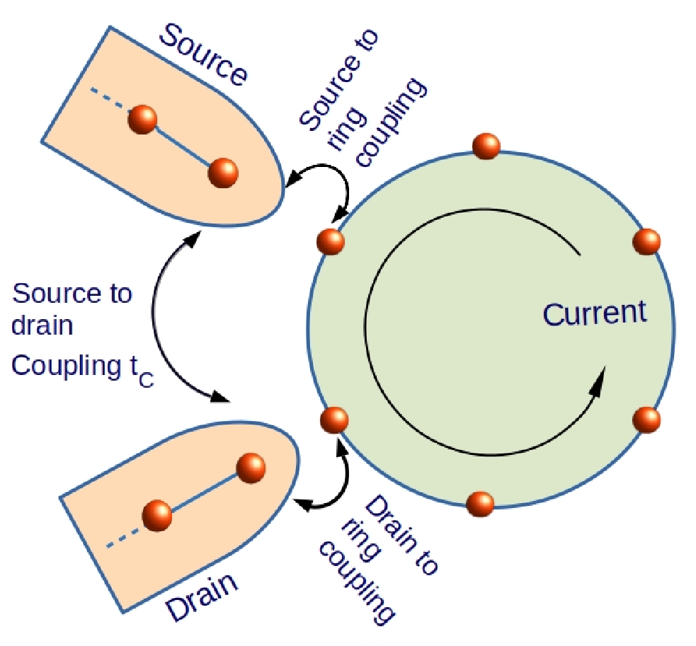
Apart from the above mentioned proposals here we present another suitable method for the proper regulations of the spin specifying input conditions. We make use of the circular current induced magnetic field to regulate the inputs and for that matter tuning of the magnetic field externally is required. We take a nano ring with two side attached metallic electrodes (S and D) connected to the two adjacent sites of the ring as shown in the left figure of Fig. 6. As the electrodes are connected at the two neighboring sites of the ring, with a finite probability, the electrons can directly hop from S to D. Let be related hopping integral between the electrodes. By changing relative positions of the electrodes we can tune , and tuning we can regulate the circular current induced magnetic field for a large scale. This proposal has already been discussed in on of our previous work ref21. For an example, taking an 20-site ring we show the variation of the magnetic field with source-to-drain coupling in the right figure of Fig. 6 where we follow the same theoretical prescription for the calculation of current and magnetic filed as described in Sec. II. From the result we can conclude that regulating the tunneling between the side attached electrodes the local magnetic field can be tuned a large scale which is required for flipping of spin states (i.e., up or down). Such nano junctions needed to be put on the sites 4 and 6 (as shown in in the right of Fig. 6, the distance of the ring center to the sites 4 and 6 will be Å ) and in every cases changing the shunting paths between source-to-drain we can specify the required input conditions.
VI Closing Remarks
In conclusion, we have theoretically realized a spin half-adder where all the inputs are output conditions are completely spin based. The outputs preserve the memories. The logic operations have been implemented in a nano channel containing multiple loops. The basic mechanism of replies on the appearance of circular current and associated magnetic field under a finite bias condition. We have used the magnetic field to rotate free spins embedded at the center of the loops. By the proper chooses of their orientations we have specified the 0 and 1 states of ‘sum’ and ‘carry’ of the half-adder. The proposal is well tested at non-zero temperature and a well suited experimental setup is discussed for input spins regulations. We have shown various other logical operation in the same setup utilizing the bias induced circular current.
In a real situation, many possible sources are there those may destroy phase and spin memory of electrons, and among them the most common source is electron-phonon (e-ph), the stray field, and other impurities. Theoretically one can incorporate these effects by studying the dephasing effecting on the current by introducing phenomenological voltage probes into the system. The effect of dephasing and impurities on circular current are different compared to the transport current, which generally decreases with these factors. On the other hand, circular current may increase in the presence of dephasing and disorder ref14. Therefore we strongly believe that the results presented here will be still valid in real experiment.
Though results displayed here are calculated for a specific system, but this proposal will be well suited for same kind of geometry having any arbitrary number of atomic sites in each loop. The spin half adder along with other logical operations, discussed here will certainly boost the new generation computations along with storage mechanism.
VII Acknowledgements
The author gratefully acknowledge the fruitful discussions with Prof. Alok Shukla and Prof. S. K. Maiti. The work has been done with the financial support (post-doctoral fellowship) from Indian Institute of Technology, Bombay, India.
Appendix A Circular current density
The wave guide formalism ref14; ref18; ref19; ref20; ref21 involves a set of linear coupled equations which are obtained from the Schrödinger equation with . The coefficients , and are the wave-amplitude corresponding to the th site of the electrodes (namely, source and drain), where as represent the site index of the ring. Let an up spin injected from the source to the channel as a plane wave with unit amplitude. For our present setup as shown in Fig. 1, we have the equations as follows:
| (272) |
The parameters and represent the coupling between source-to-channel and channel-to-drain, respectively. and are to the reflection and transmission probabilities, respectively. be the polar angle whereas is the azimuthal angle. is wave vector and is the atomic length. By solving Eq. 272, we get bond current densities for sites and of the channel as:
| (273) |
In the above expressions, is used for the incident spin, while represents the transmitting spin.
Similarly, for the down spin incidence, we get a set of equations like Eq. 272 and we evaluate and . With all these components of circular bond current densities now we define the net bond current density as .
References
- (1) S. Datta, Lessons from Nanoelectrctonics: A New Perspective on Transport (World Scientific, 2012).
- (2) S. Bandyopadhyay and M. Cahay, Nanotechnology 20, 412001 (2009).
- (3) S. Datta and B. Das, Appl. Phys. Lett. 56, 665 (1990).
- (4) H. J. Zhu et al., Phys. Rev. Lett. 87, 016601 (2001).
- (5) A. T. Hanbicki et al., Appl. Phys. Lett. 82, 4092 (2003).
- (6) X. Jiang et al., Phys. Rev. Lett. 94, 056601 (2005).
- (7) S. A. Crooker et al., Science 309, 2191 (2005).
- (8) X. Lou et al. Nature Phys. 3, 197 (2007).
- (9) Y. Ohno et al. Nature 402, 790 (1999).
- (10) T. Dietl, H. Ohno, F. Matsukura, J. Cibert, and D. Zener Ferrand, Science 287, 1019 (2000).
- (11) S. A. Wolf et al., Science 294, 1488 (2001).
- (12) D. E. Nikonov, G. I. Bourianoff, and P. A. Gargini, J. Supercond. Novel Magn. 19, 497 (2006).
- (13) M. Johnson and R. H. Silsbee, Phys. Rev. Lett. 55, 1790 (1985).
- (14) M. N. Baibich et al., Phys. Rev. Lett., 61, 2472 (1988).
- (15) A. Ney, C. Pampuch, R. Koch, and K. H. Ploog, Nature 425, 485 (2003).
- (16) H. Dery, P. Dalal, L. Cywiski and Ł. J. Sham, Nature, 447 573 (2007).
- (17) B. Behin-Aein, D. Datta, S. Salahuddin, S. Datta, Nature Nanotech. 6, 266 (2010).
- (18) M. Kazemi, Sci. Rep., 7 15358 (2017).
- (19) A. A. Khajetoorians, J. Wiebe, B. Chilian, and R. Wiesendanger, Science 332, 1062 (2011).
- (20) D. Rai, O. Hod, and A. Nitzan, J. Phys. Chem. C 114, 20583 (2010).
- (21) D. Rai, O. Hod, and A. Nitzan, Phys. Rev. B 85, 155440 (2012).
- (22) M. Patra and S.K. Maiti, Sci. Rep. 7 43343 (2017).
- (23) M. Patra and S. K. Maiti, Org. Electron. 62, 454 (2018).
- (24) M. Patra and S. K. Maiti, Phys. Rev. B 100, 165408 (2019).
- (25) K. Tagami, M. Tsukada, Curr. Appl. Phys. 3 439 (2003).
- (26) M. Patra, A. Shukla, and S. K. Maiti, J. Phys. D: Appl. Phys. 54, 095001 (2021).
- (27) H. Cai et al., Appl. Sci. 7, 929 (2017).
- (28) B. J. Shields, Q. P. Unterreithmeier, N. P. de Leon, H. Park, and M. D. Lukin, Phys. Rev. Lett. 114, 136402 (2015).
- (29) J. Wabnig and B. W. Lovett, New J. Phys. 11, 043031 (2009).
- (30) R. Hanson and D. D. Awschalom, Nature 453 1043 (2008).
- (31) J. R. Maze et al., Nature 455 644 (2008).
- (32) M. Sarovar, K. C. Young K C, T. Schenkel and B. K. Whaley, Phys. Rev. B 78, 245302 (2008).
- (33) H-Z Lu and S-Q Shen, Phys. Rev. B 77, 235309 (2008).
- (34) M. Patra and S. K. Maiti, Europhys. Lett. 121, 38004 (2018).
- (35) D. A. Lidar and J. H. Thywissen, J. Appl. Phys. 96, 754 (2004).
- (36) S. Datta, Electronic Transport in Mesoscopic Systems (Cambridge University Press, Cambridge, 1997).
- (37) S. Datta, Quantum Transport: Atom to Transistor (Cambridge University Press, Cambridge, 2005).
- (38) S. K. Maiti, J. Appl. Phys. 117, 024306 (2015).
- (39) F. H. L. Koppens, K. C. Nowack, and L. M. K. Vandersypen, Phys. Rev. Lett. 100, 236802 (2008).
- (40) Y. Tokura, W. G. van der Wiel, T. Obata, and S. Tarucha, Phys. Rev. Lett. 96, 047202 (2006).
- (41) K. C. Nowack, F. H. L. Koppens, Y. V. Nazarov, and L. M. K. Vandersypen, Science 318, 1430 (2007).
- (42) K.-M. C. Fu, S. M. Clark, C. Santori, C. R. Stanley, M. C. Holland, and Y. Yamamoto, Nat. Phys. 4, 780 (2008).
- (43) J. Berezovsky, M. H. Mikkelsen, N. G. Stoltz, L. A. Coldren, and D. D. Awschalom, Science 320, 349 (2008).
- (44) Y. Wu, E. D. Kim, X. Xu, J. Cheng, D. G. Steel, A. S. Bracker, D. Gammon, S. E. Economou, and L. J. Sham, Phys. Rev. Lett. 99, 097402 (2007).
- (45) D. Press, T. D. Ladd, B. Zhang, and Y. Yamamoto, Nature 456, 218 (2008).
- (46) C.-M. Ryu, S. Y. Cho, M. Shin, K. W. Park, S. Lee, and E.-H. Lee, Int. J. Mod. Phys. B 10, 701 (1996).
- (47) Y. Shi and H. Chen, Phys. Rev. B 60, 10949 (1999).
- (48) Y.-J. Xiong and X.-T. Liang, Phys. Lett. A 330, 307 (2004).
- (49) M. Patra and S. K. Maiti, Sci. Rep. 7, 14313 (2017).