Realization of the Chern insulator and Axion insulator phases in antiferromagnetic MnTe-Bi2(Se, Te)3-MnTe heterostructures
Abstract
Breaking time-reversal symmetry in three-dimensional topological insulator thin films can lead to different topological quantum phases, such as the Chern insulator (CI) phase, and the axion insulator (AI) phase. Using first-principles density functional theory methods, we investigate the onset of these two topological phases in a tri-layer heterostructure consisting of a Bi2Se3 (Bi2Te3) TI thin film sandwiched between two antiferromagnetic MnTe layers. We find that an orthogonal exchange field from the MnTe layers, stabilized by a small anisotropy barrier, opens an energy gap of the order of 10 meV at the Dirac point of the TI film. A topological analysis demonstrates that, depending on the relative orientation of the exchange field at the two interfaces, the total Chern number of the system is either or , characteristic of the CI and the AI phase, respectively. Non-topological surface states inside the energy-gap region, caused by the interface potential, complicate this identification. Remarkably though, the calculation of the anomalous Hall conductivity shows that such non-topological surface states do not affect the topology-induced transport properties. Given the size of the exchange gap, we estimate that gapless chiral edge states, leading to the quantum anomalous Hall effect, should emerge on the sidewalls of these heterostructures in the CI phase for widths nm. We also discuss the possibility of inducing transitions between the CI and the AI phases by means of the spin-orbit torque caused by the spin Hall effect in an adjacent conducting layer.
I Introduction
The discovery of three-dimensional (3D) topological insulators (TIs), characterized by a bulk band gap and dissipationless helical surface states protected by the time-reversal symmetry (TRS), has led to intense research in topological materials over the past decadeKane and Mele 2005; Bernevig et al. 2006; König et al. 2007; Hasan and Kane 2010; Bansil et al. 2016. Introducing magnetic order in TIs breaks TRS, an exchange energy gap opens up at the Dirac point (DP) of the topological surface states, and different topological phases emerge when the chemical potential is tuned inside the gapHe et al. 2013; Tokura et al. 2019. Magnetism in TIs can be achieved either by doping with magnetic impuritiesZhang et al. 2013; Fan et al. 2019; Kim et al. 2017; Islam et al. 2018; Tokura et al. 2019; Satake et al. 2020 or through proximity with magnetic layersLuo and Qi 2013; Eremeev et al. 2013; Wei et al. 2013; Lee et al. 2016; Burn et al. 2019. Recently, intrinsic magnetic TIs such as the van der Waals layered MnBi2Te4-familyOtrokov et al. 2017; Li et al. 2019; Otrokov et al. 2019 and Mn4Bi2Te7 Hirahara et al. 2020 have also been discoverednot. Magnetic TIs host a wide range of novel quantum phenomena, of which the most important and most investigated ones are the quantum anomalous Hall effect (QAHE) and the topological magneto-electric effect (TME)Hasan and Kane 2010. The common origin of these phenomena is the so-called topological -axion termWilczek 1987, which in TIs has to be added to the ordinary Maxwell electrodynamicsQi et al. 2008; Essin et al. 2009. In 3D TIs, the -term is directly related to the topological index , and can only affect the 2D Dirac surface states. When TRS is broken at the surface of a TI, a half-integer quantum anomalous Hall conductivity ( is the Planck constant and is the electron charge) arises at that surfaceFu and Kane 2007; Qi et al. 2008; Essin et al. 2009; Vanderbilt 2018.

In a TI thin film, the resulting topological state depends on how TRS is broken at the two surfaces, see Fig. 1. Specifically, when the magnetization at the top and the bottom surfaces points in the same direction (P configuration) and the chemical potential is inside the exchange gap, the system is in the Chern insulator (CI) state. This phase is characterized by a non-zero integer Chern number , and may display the QAHE in which the Hall conductance in a Hall bar geometry is quantized , due to the emergence of chiral edge states on the film side wallsYu et al. 2010; Chang et al. 2013; Liu et al. 2016; Chang and Li 2016. On the other hand, when the magnetization at the top and bottom surfaces points in opposite directions (AP configuration), the system is in the axion insulator (AI) state where . In this phase, all the surface states are gapped, and transport in a Hall bar geometry is characterized by a large longitudinal and zero Hall resistance. A quantized version of the magnetoelectric coupling (the TME) with a universal coefficient equal to is predicted by theory Qi et al. 2008; Essin et al. 2009; Wang et al. 2015; Morimoto et al. 2015; Armitage and Wu 2019; Vanderbilt 2018, where an applied magnetic field causes a response in the electrical polarization and vice versa.
Recent experimental work shows that both the CI and AI phases can be realized in magnetic modulation-doped TI multilayer films Mogi et al. 2017; Xiao et al. 2018; Allen et al. 2019. However, the magnetic gaps in these doped-TI thin films are small, and the presence of impurity statesSessi et al. 2016; Islam et al. 2018 as well as the dissipative non-chiral edge states inside these gaps Pertsova et al. 2016 limit substantially the maximum temperatures and magnetic field intervals where the CI and AI phases are stable. These are also some of the reasons that have so far precluded the realization of the much more elusive TME in the AI phase.
An alternative approach to generate uniform 2D magnetism at the surfaces of a TI thin film is to exploit the interfacial proximity with an adjacent film of a magnetic insulator or semiconductorLuo and Qi 2013; Eremeev et al. 2013; Wei et al. 2013. The crucial issues here are the selection of the best magnetic materials, and the nature of their coupling with the TI film. The magnetic layer should be able to generate sizable exchange gaps; at the same time, the interface hybridization should not be too strong to avoid damaging the Dirac surface states or shifting them away from the Fermi level. For this purpose, over the past few years, several magnetic insulator-TI heterostructures have been proposed theoretically and realized experimentallyYang et al. 2013; Lang et al. 2014; Katmis et al. 2016; Tang et al. 2017; Hirahara et al. 2017; Zhu et al. 2018; Mogi et al. 2019. The majority of these consist of ferromagnetic (FM) insulators, but a few examples with antiferromagnetic (AFM) materials have been consideredLuo and Qi 2013; Eremeev et al. 2013; He et al. 2018; Yang et al. 2020; Bonbien et al. 2021. Despite all this effort, realization of the CI and AI phases in these heterostructures is still quite challenging, and only very recently the first observation of the QAHE in a FM/TI/FM tri-layer heterostructure has been reportedWatanabe et al. 2019.
In this paper, we employ density functional theory (DFT) to study the electronic and topological properties of an AFM/TI/AFM tri-layer heterostructure, where the hexagonal manganese telluride semiconductor, is used to magnetize the Dirac surface states of two prototypical 3D TIs: Bi2Se3 and Bi2Te3. The goal of this work is to investigate the possibility of realizing both the CI and AI phases within the same heterostructure, and introduce efficient ways of switching between these two phases. MnTe is a material that had been extensively studied in the pastKomatsubara et al. 1963, but it has received great renewed attention recently for its relevance to AFM spintronicsKriegner et al. 2016; Kriegner et al. 2017. Its magnetic structure consists of FM hexagonal Mn planes which are antiferromagnetically coupled along the c axis (growth direction). AFM insulators have an advantage over FM insulators in that their stray magnetic field, which has detrimental effects at the interface, is considerably smaller than the field of FM insulators. Stray magnetic fields can also introduce spurious effects in the study of the QAHE and the TME.
The tri-layer heterostructure considered here allows us to realize the two mentioned CI and AI phases shown in Fig. 1. We find that the magnetic anisotropy energy due to the AFM layers favors an out-of-plane easy axis (i.e., orthogonal to the surface) with an energy barrier of meV. The resulting orthogonal exchange field generates an energy gap of the order of 10 meV at the DP of the surface states of the TI film, which should be viewed as fairly large for this type of heterostructure. The topological analysis fully supports the expectation that in the P configuration the system has Chern number , whereas in the AP configuration . Importantly, the bandstructures for both phases show the emergence of non-topological surface states in the region of the DP, caused by the interface potential. This feature confirms that engineering a heterostructure in which the magnetic layers only provide gap-opening exchange fields remains a challenging task. Nevertheless, a calculation of the anomalous Hall conductivity shows that, for the heterostructure considered here, such non-topological surface states do not disrupt the transport properties that depend on the topological invariants. Atomistic tight-binding calculations with parameters extracted from the DFT results show that a nanoribbon with width of nm cut out of the heterostructure does support chiral edge states in the CI phase.
The paper is organized as follows: in Sec. II we describe the details of the computational procedure employed in this work. The results of the electronic structure, topological analysis and investigation of the chiral edge states are presented in Sec. III. In Sec. IV we discuss an electric mechanism based on the spin-orbit torque, which can be used to promote topological phase transitions from the CI to the AI phase in a topological memory device. Finally, in Sec. V we present our conclusions.
II Computational details
II.1 First-principles DFT calculations
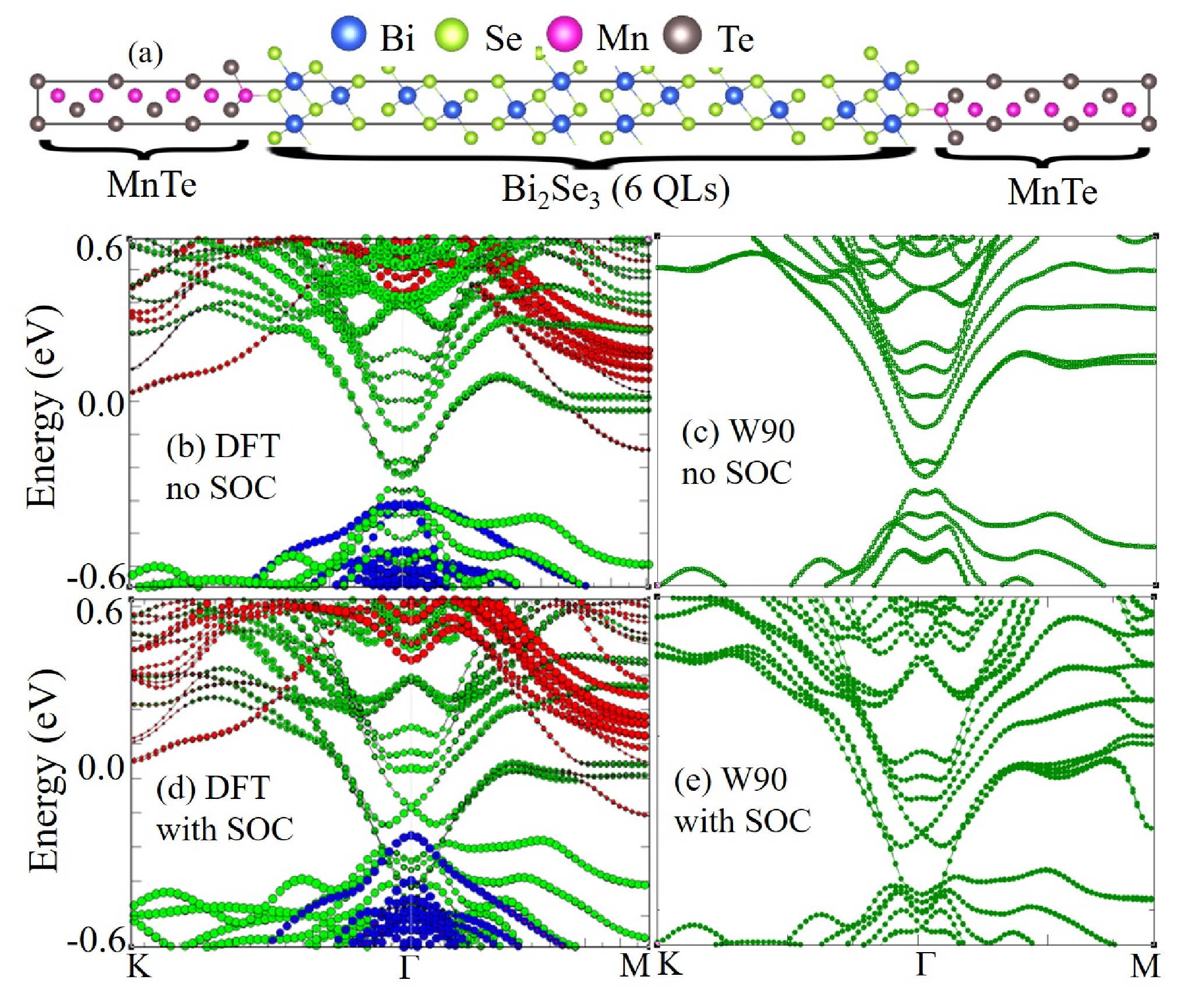
To study the electronic and topological properties of MnTe-Bi2(Se, Te)3-MnTe heterostructure, we have constructed a periodic supercell (no vacuum) consisting of six quintuple layers (QLs) of Bi2(Se,Te)3 TI sandwiched between two MnTe films with each film containing three unit cells of MnTe as shown in Fig. 2a to preserve the inversion symmetry. The termination of the MnTe at the interface plays a critical role in magnetizing the TI surface statesYang et al. 2020. Since the Mn atoms provide the exchange coupling to open the gap at the DP, we have placed the Mn layer of MnTe film closest to the TI material to have a stronger impact. However, the Mn atoms can be coupled to the topmost TI layer in two different configurations: i) a top-site setup, where the Mn atom is aligned with the Se (Te) atoms (see Fig. 2a); ii) a hollow-site setup, where Mn is aligned with the Se (Te) atoms at the second layer of the TI. We have found that the top-site setup is energetically favorable. Therefore, all the self-consistent calculations in this work are performed using the top-site setup.
All the DFT calculations are performed by employing the Vienna ab initio Simulation Package (VASP)Kresse and Hafner 1993; Kresse and Furthmüller 1996, and using the Perdew-Burke-Ernzerhof generalized gradient approximation (PBE-GGA) for the exchange correlation functionalPerdew et al. 1996. We have first relaxed the crystal structure for both the cell parameters and the atomic positions using a -mesh of size 6 6 1 until the stress on the cell and the average forces on the atoms are 0.02 eV/Å.
The final relaxed structure is then used to study the electronic properties with the inclusion of the spin-orbit coupling (SOC); for this part we use a larger -mesh of 10 10 1 to improve the accuracy of the calculations. To incorporate the effect of correlations at the transition metal Mn atoms, all self-consistent calculations are performed using GGA+U with =4 eV.
II.2 Tight-binding Models
For the topological studies of this system, we have constructed a real-space tight-binding (TB) Hamiltonian in the basis of the Wannier states for the low-energy bands extracted by Wannier90 Mostofi et al. 2014. We would like to point out that, to our best knowledge, the construction of a TB model directly from DFT calculations for such a complicated system was never done before. The accurate construction of the WFs of this complex structure is computationally very challenging, particularly with SOC. For this reason, we have implemented the following strategy. We have first calculated the KS orbitals without SOC. Since the DFT calculations show that the states near the DP are predominantly the states of Bi and Se (Te) atoms of the TI part of the heterostructure, we have projected the Bloch states onto these -orbitals. Thus, for our system we have constructed a total number of 90 WFs for each of the two spin states (up and down). To ensure that these functions are atomic-like orbitals localized on their respective sites, we have used up to 260 bands, which resulted in WFs with a spread of about 3 Å2 or less, compatible with the spreads of the pristine compounds. To reduce the numerical error during the Wannierization, we have also implemented disentanglement, a procedure to project out the contribution of the relevant bands from the unwanted bandsSouza et al. 2001. The condition that must be satisfied for this approach to work is the possibility of disentangling the p-bands of the TI from the bands of the magnetic layer. This is possible with the MnTe but not for transition metal pnictides such as CrSb. Indeed, we also have tried other heterostructure e.g., CrSb-Bi2(Se, Te)3-CrSb, but we were unable to disentangle the -bands of the TI from the bands of the magnetic layer. The transition metal pnictides like CrSb show negligible charge transferPark et al. 2020; as a consequence, the -bands of the transition metals are at the Fermi level. Moreover, these -bands cannot be disentangled from the -bands of the pnictidesCuono et al. 2019.
Since the WFs are constructed from the DFT bands which include the structural and magnetic effects of all atoms, these WFs also include the effects of the MnTe films. We would also like to mention that in this approach we have not implemented the procedure for Maximally Localized Wannier Functions since such a procedure leads to a mixing of different orbitals, making the use of atomic SOC constants in constructing the TB Hamiltonian with SOC unfeasible.
The effective TB Hamiltonian containing the effect of the exchange field obtained from this calculation is then used to construct the Hamiltonian with SOC. The acceptable accuracy of the TB Hamiltonian is determined by the criterion that the bands obtained from this Hamiltonian should be a good match with the corresponding bands obtained from the full DFT calculations when SOC is also included. The inclusion of the SOC into the TB Hamiltonian affects the -orbitals of the Bi and Se (Te) atoms with a coupling, atomic in character, whose strength is given by possibly renormalized atomic SOC parameters . Our calculations show that a good match of the bands can be obtained with =1.60 and =0.34 for Bi2Se3 TI. On the other hand, for Bi2Te3 TI, only a small adjustment of the original atomic parameters is required (=1.2 eV and =0.5 eV. Note that the corresponding atomic values of the SOC parameters are =1.25 eV, =0.49 eV, and =0.22Wittel and Manne 1974). Figs. 2b-e show the comparison of the bands obtained from DFT and the Wannier90 TB calculations. A good match implies that the topological properties can be reliably calculated from the TB Hamiltonian.
II.3 Topological Chern numbers
The topological properties of the system with broken TRS are characterized by the Chern number, which can be calculated either by integrating the total Berry curvature over the 2D Brillouin zone (BZ) or by integrating the Berry connection over the boundary of the 2D BZ:
| (1) |
where
| (2) |
with
| (3) |
Here are Bloch states with energies and the sum in Eq. 3 is over all occupied states, defined by putting the Fermi energy inside the exchange gap.
By introducing the velocity operator with components , the Berry curvature can be rewritten as
| (4) |
where now the sum in Eq. 4 is over both occupied and unoccupied states.
The expression of the Chern number given by the line integral of can be reformulated in terms of Wannier Charge Centers (WCC), localized along the -direction, which are defined bySoluyanov and Vanderbilt 2011
| (5) |
The approach in terms of WCC is particularly convenient for the numerical evaluation of the Chern number, as implemented in WannierToolsWu et al. 2018; it is this procedure that we have used in our work. Nonetheless, the alternative expression of the Berry curvature given in Eq. 4 will be very useful for the microscopic interpretation of the Chern number and for understanding the conditions of validity of the method.
Strictly speaking, the Chern number is a well-defined integer only when the Fermi energy lies between Bloch state bands. In this case, the anomalous Hall conductance of 2D systems is equal to the quantized value in units of . As we explained in Sec. II.A, the first-principles DFT calculations reported here are carried out on bulk 3D systems, where the 2D heterostructure is periodically repeated in the -direction. However, the topological Chern number is evaluated by means of the effective 2D TB model, corresponding to selecting the -plane in the BZ.
III Results
III.1 Electronic and magnetic properties of the MnTe-Bi2(Se, Te)3-MnTe heterostructures
In this work we have investigated two different heterostructures, namely MnTe-Bi2Se3-MnTe and MnTe-Bi2Te3-MnTe. Since the most important effect caused by the AFM MnTe layers, namely the magnetization of the surface states and the opening of an energy gap at their DP, is expected to occur predominantly only when the exchange field is orthogonal to the surface of the heterostructure, we will assume for the time being that this direction of the exchange fields is the one that corresponds to the lowest energy state of the system. At the end of this section we will show that, by calculating the magnetic anisotropy energy, the system has indeed an out-of-plane easy axis with a small energy barrier meV.
The presence of the magnetic films is expected to open up a gap at the DPs, but it can also modify the orbital properties of the surface states, which can play a crucial role in determining the topological properties. Therefore, we first discuss how the overall electronic structure and, in particular, the Dirac surface states of a pristine Bi2Te3 slab are modified by the magnetic films at the two interfaces.
In Fig. 3a and b we have plotted the bandstructure of pristine Bi2Se3 and MnTe-Bi2Se3-MnTe, respectively, highlighting the contribution of different QLs (first, second and third) of Bi2Se3. Note that only the first three top QLs of the TI film QLs are shown, the second three being identical by mirror symmetry with respect to the plane in the middle of the TI film. It is evident that the first and the second QL closest to the two interfaces provide most of the contribution to the Dirac surface states (note the linear dispersion region inside the box) of pristine Bi2Te3, with the largest contribution coming from the 1st QL. The contributions from the 3rd QL to the surface states are vanishingly small, and therefore these QLs may be viewed to involve bulk states only. In the heterostructure, on the other hand, we find the following outstanding features:
- (i)
Due to the closest proximity to the MnTe film, the atomic orbitals of the first QL hybridize with the magnetic film and decouple from the surface states, which now reside mostly on the atoms of the second QL.
- (ii)
Importantly, as a result of the shift of the surface states from the first QL to the second, the DP, which was at the Fermi level for the pristine TI film, moves below the Fermi level by approximately eV.
- (iii)
As a result of interface potential, a new non-topological surface state appears, localized on the very first QL of the TI film. See top panel of Fig.3(b). Given its immediate proximity with the magnetic layer, this surface state is strongly spin polarized. At the -point, the energy band of this state drops deeply inside the bulk states and it has a gap of meV. Away from the -point, this band extends inside the bulk gap, and couples strongly with the topological surface states. It is via this coupling that the topological surface states, now not directly in contact with the magnetic layers, will acquire a gap (see below). We will also see that the presence of this non-topological band inside the energy region of the DP represents an important challenge in realizing the CI and the AI topological phases.
- (iv)
Very similar features are also found for the MnTe-Bi2Te3-MnTe heterostructure.
The space shift of the topological surface states from the first to the second QL, and the emergence of a non-topological bound state at the interface as a result of the crystal symmetry breaking at the interface, were already pointed out in Ref. Eremeev et al. 2013 for the study of the Bi2Se3/MnSe heterostructure.

We now discuss the effect of magnetism on the topological surface states due to the magnetic film. For each of these two heterostructures, we have studied both the P and AP magnetic configurations (see Fig. 1), between the exchange fields of the MnTe films at the two interfaces (see Figs. 4a and b). Our calculations show that the AP configuration is lower in energy compared to the P configuration by about 9 meV in Bi2Se3 and by 1 meV in Bi2Te3 TIs. However, this difference in energy is due to the exchange interaction between the magnetic films of the neighboring supercells in our bulk-like approach, that is, it is not a property of the magnetic coupling of the two MnTe films in the isolated heterostructure. To estimate the magnetic interaction between two interfaces, we have performed a calculation by adding a vacuum of about 16 Å between the two supercells, which shows that both the P and the AP configurations are almost degenerate (AP is lower in energy than P by less than 0.1 meV).

In Figs. 4c and d we have plotted the bandstructure of MnTe-Bi2Te3-MnTe for the P and AP configurations. The bandstructure of the MnTe-Bi2Se3-MnTe heterostructure (not shown here) is qualitatively identical (see Fig. 2d). We observe the following salient features.
The bandstructure of the P and AP configurations are qualitatively very similar, with one important distinction (see Fig 4(c)-(d)). The Dirac point of Bi2Te3 (Bi2Se3) TI resides at about 0.13 eV (0.17 eV) below the Fermi level due to the presence of MnTe films at the two interfaces.
For both configurations, breaking of the TRS at the surface of the TI by the MnTe film opens up a gap at the DP of the TIs, as shown in Fig 4(e)-(f) where we zoom in the region around the DP. Although MnTe is an AFM insulator and therefore has no net magnetization, it can provide an effective FM exchange coupling at the interface with the following mechanism: since the first FM layer of Mn atoms is the closest to the TI surface, its Mn states are exchange coupled with the states of the surface electrons within the first QL of the TI, resulting in a FM spin polarization of the surface states (residing on this first QL) along the magnetization direction of the magnetic film. An exchange gap then opens up at the DP due to the overlap between the spin-polarized non-topological surface states (the states outside the box in Fig. 3b) and the topological surface states residing on the second QLEremeev et al. 2013. These spin-polarized surface states have a small but non negligible contribution to the topological surface states, which also contribute to the gap opening at the Dirac point. The second magnetic layer, which is anti-parallel to the first layer, can also contribute to the exchange field in the opposite sense. But since it is about 2.6 Å away from the first layer, its contribution is exponentially smaller than the other. Therefore, the contribution to the exchange gap at the DP essentially results from the closest Mn layer. Our calculations show that the gap at the DP of MnTe-Bi2Te3-MnTe heterostructure is about 12 meV, whereas for MnTe-Bi2Se3-MnTe heterostructure, it is about 7 meV.
Although the bandstructures of the P and AP configurations are quite similar, there is a noticeable qualitative difference, albeit quantitative small, as shown in Fig 4(e)-(f) by zeroing inside the region of the split DP. The energies in this region originate from two Dirac-cone surface states (one from the top and one from the bottom interface). We can see that these energies are exactly two-fold degenerate for the AP configuration, whereas for P configuration this degeneracy is lifted. Disregarding for a moment the complications caused by the hybridization with the states of the AFM layers, we can explain this result in the following way. The exchange interaction at the two surfaces spin polarizes the surface states around the point of the two Dirac cones and opens a magnetic gap separating “valence” majority-spin states (lower in energy) from “conduction” minority-spin states (higher in energy). In the P configuration, the valence bands of the two cones, degenerate in energy, have also the same spin-character and so do the two conduction bands. Therefore in a thin film, any tunneling between the top and bottom surface can couple these degenerate states, and lift the degeneracy by creating bonding and anti-bonding states. In the AP configuration, the two valence and two conduction bands have an opposite spin character at the point and cannot couple directly. In principle, the valence band of the top surface can couple with the conduction band of the bottom surface and vice versa. However, apart from being a smaller effect since they have different energies, this coupling still generates pairs of perfectly symmetric splitting, and therefore the energies remain two-fold degenerate.
A careful inspection of the energy bands shows that in the AI phase the spectrum of the whole heterostructure is exactly degenerate everywhere. This degeneracy stems from the perfect mirror symmetry (included the direction of the magnetization at the interfaces) with respect to a plane located in the middle of the heterostructure. Alternatively, the overall symmetry behind this degeneracy can be viewed as the product of inversion (with respect to the origin located in the middle of the heterostructure) and time-reversal . Clearly, the AI phase is symmetric under , whereas the CI is not.
The consequence of the degeneracy is also reflected into the spin texture of the surface states, as shown in Figs. 4g-h, where we have plotted the expectation value of the spin along a closed loop in -space around the -point at constant energy eV, just above the DP. It is evident from the figure that for the P configuration the spin states associated with the top and the bottom surface states are split in the momentum space, and form a spiral spin texture with opposite helicity. On the other hand, for the AP configuration, these two helical spin states are degenerate in the momentum space.
In order to gain insight into the gap difference for the two heterostructures, we have calculated the potential energy distribution across the interface, averaged over the xy-plane as a function of the distance along the growth direction (z), and have analyzed the effect of the interface potential on the wave function of the surface electrons. In Fig. 5, we have plotted the potential profile and the wave function of a surface electron close to the DP. We note that for Bi2Se3 the peak of the potential is shifted slightly towards the bulk. However, for Bi2Te3 the potential profile is rather uniform across different QLs. The uniformity is due to the fact that the Te atom is common to both TI and magnetic film. Therefore, the structure may be viewed as a continuation of the TI material with some Bi atoms replaced by Mn atoms resulting in a weak interface effect compared to Bi2Se3. As a consequence, the wave function of the surface electrons of Bi2Se3 is pushed towards the bulk (extended up to the third QL), similar to the one obtained for the Bi2Se3-MnSe heterostructureEremeev et al. 2013. For Bi2Te3 the wave function is essentially localized between the first and the second QLs, which is consistent with the surface wave function of pure TI materials with no interface effectPertsova and Canali 2014. Since the surface electrons in Bi2Te3 are closer to the magnetic film, they experience a larger effective exchange field, resulting in a larger gap at the DP compared to that of Bi2Se3.

Realization of the quantum phases CI and AI in magnetic TIs requires opening of an energy gap at the DP. The simplest Dirac model of the topological surface states with linear dispersion predicts that the presence of a TRS breaking exchange field opens a gap only when the magnetization is orthogonal to the surface. It turns out that it is also possible to open a gap when the magnetization is in-plane by means of other mechanisms. When the magnetization lies in the plane of the surface, it shifts the DP from the -point along a direction perpendicular to the magnetization. A gap then opens up at the shifted DP due to non-linear corrections to the simple Dirac model that are also responsible for the hexagonal warping of the dispersionFu 2009; Islam et al. 2019. However, such a gap is typically smaller compared to the gap induced by an out-of-plane magnetization. Therefore, to assess which mechanism is relevant for the heterostructures investigated in this work, we have calculated the magnetic anisotropy energy of the two heterostructures. Magnetic anisotropy calculations are computationally very subtle because they involve small energy differences between the (large) ground state energies for different orientations of the magnetization. To attain the required accuracy in the total energy for a given magnetization orientation, we have used 16 16 1 -mesh f or this calculation. Our calculations show that, for both Bi2Te3 and Bi2Se3 heterostructures, the ground state magnetization is oriented along the out-of-plane direction, namely we have an easy axis along the -direction, with an anisotropy barrier of 0.5 meV and 0.6 meV respectively. It is interesting to note that the magnetization of bulk MnTe lies in-planeKriegner et al. 2017 with a small anisotropy of 0.2 meV, but the interaction of the magnetic film with the surface electrons of the TI (- hybridization) and the change in lattice constant with respect to the bulk MnTe, rotate the magnetization along the out-of-plane direction. The obtained anisotropies, of the order of 0.3 meV per two Mn atoms are one of the largest values obtained in DFT; there are very few systems like Fe/Pt where one can get higher values. Actually, these anisotropies would allow the stability of the two phases at 4 K. Note that the majority of the experiments on the QAHE in TI system are done at sub-Kelvin temperatures.
III.2 Topological properties of MnTe-Bi2(Se, Te)3-MnTe heterostructures
In this section, we investigate whether the tri-layer AFM/TI/AFM heterostructure consisting of the AFM semiconductor MnTe and the TI Bi2Se3 or Bi2Te3 can provide a platform to realize both the AI and CI phases within the same system, as a result of the effect of 2D magnetism on the TI surface states. Topologically, these two phases are characterized by a total Chern number and respectively. Therefore, we have calculated the total Chern number for both the P and AP configurations. To set up the calculation, we first construct a set of Wannier functions from the DFT result, which are then used to construct the TB Bloch Hamiltonian. The details of this computational procedure are described in Sec. II.
In applying this procedure to our two heterostructures, we face the following problem. As we can see from the bandstructure plotted in Fig. 4, if we set the chemical potential inside the exchange gap, the highest occupied “valence” band, which at the point is the highest band below , will eventually cross at some finite . Therefore, strictly speaking, is not well defined. However, a close inspection shows that the highest occupied band at the always maintains a finite gap with the band immediately above (which is the first unoccupied “conduction” band at the point) throughout the BZ. Therefore, we can formally still apply the procedure given in Eq. 4, and obtain a topological characterization of the valence energy bands, by assuming that the highest “occupied” and the lowest “unoccupied” bands are the ones defined at the point. Note that this procedure was used in Ref. Fu and Kane 2007 to calculate topological invariants for 3D TIs which present a finite direct energy gap throughout the BZ but a negative indirect gap due to band overlap. In agreement with the expectations, our calculations show that for the P configuration and for the AP configuration for both heterostructures. This result demonstrates that the P and AP configurations give rise to two topologically distinct states which are consistent with the CI phase and the AI phase, respectively.
To elucidate further the distinct topological character of the P and AP configurations and support the claim that the AP configuration does correspond to the AI phase, we have investigated the 3D anomalous Hall conductivity (AHC). The AHC can be calculated directly from the Kubo formula in terms of eigenstates and eigenvalues of the Bloch HamiltonianNagaosa et al. 2010
| (6) | |||||
where is the Fermi-Dirac distribution function for a given chemical potential . From a comparison with Eq. 4, we can see that is proportional to the integral of the Berry’s curvature over the 3D Fermi sea, and therefore it is directly related to the topological properties of the Bloch states.
In Fig. 6 we have plotted as a function of chemical potential . Note that integral in Eq. 6 is over the 3D Brillouin zone; the units of the 3D conductivity are in . The figure shows that when lies inside the exchange gap, delimited by the values and , for the AP configuration [Fig. 6(a)], which is consistent with the topology-controlled transport properties expected for the AI phase. On the other hand, for the P configuration [Fig. 6(b)], displays a constant value -0.25 when is inside the exchange gap, which would correspond to 2D conductance of the order of the quantized value for a few-nanometer-thick thin film. It is quite remarkable that the presence of non-topological states in the exchange gap region (albeit away from the DP) does not seem to disrupt these topological features for both configurations, suggesting that these states do not contribute to the overall Berry’s curvature.

As the reaches the top and bottom edge of the exchange gap, we observe the emergence of two sharp peaks in for both spin configurations. This occurrence can be ascribed to the -dependence of the Berry’s curvature, which is sharply peaked at the point. Therefore, the main contribution to in Eq. 6 involves the coupling between the occupied and unoccupied states at , with the small energy denominator , which is possible only when is inside the exchange gap (see insets of Fig. 6). Clearly this contribution drops out precisely when or . Outside the gap region is identically zero for the AP configuration; for the P configuration is typically finite but not quantized.
At this point it is important to address the question of whether the topological and transport properties presented here are an incontrovertible proof that both the CI and AI phase are in fact realized in these heterostructures. The non-zero Chern number and the quantized value of found in the P configuration is a strong indication that this configuration is indeed a CI phase. The case for the AI phase in the AP configuration is more subtle, since and = 0 could as well correspond to a trivial insulator with TRS broken at the surface. Here the only real proof for the AI phase would be the existence of a half quantized Hall conductance with opposite signs at the top and bottom surface. We are unable to carry out these calculations with the present version of WannierTools. Nevertheless, it is very unlikely that flipping the magnetization from P to AP, which results in only minor changes in the band structure, should bring about a topological phase transition from a CI to a trivial insulator. Therefore we believe that the case for the AI phase in the AP configuration is equally quite strong.
A non-trivial gap at the DP, characterized by different topological invariants for the CI and AI phases, has different observable consequences. For a heterostructure of finite width, the non-zero Chern number, characterizing the CI phase, results in one dimensional (1D) dissipationless chiral edge states appearing on the sidewalls, leading to the QAHE (see Fig. 1). On the other hand, in the AI phase, these chiral edge states are absent, and provided that no additional non-topological 1D conducting states appear on the sidewalls, and all the surfaces are insulating; this is one of the essential condition for the realization of the quantized TME.
To ascertain some of these physical consequences in the MnTe/Bi(Se,Te)/MnTe heterostructures, we have investigated the heterostructures in a quasi 1D nanoribbon geometry, with a finite width of the order of several tens nm. The goal is to see the emergence of chiral edge states on the sidewalls of the nanoribbon when the system is in the P configuration corresponding to the CI phase. Unfortunately, the presence of non-topological surface states in the gap region of the 2D bandstructure (localized in the first QL, see Fig. 3), when projected along the edge of the nanoribbon, generates additional non-topological 1D states, blurring the detection of the topological chiral edge states.
We have then resorted to the less ambitious goal of assessing the presence and nature of topological chiral edge states in a magnetic TI nanoribbon in the CI phase, with the same exchange gap found by DFT for the realistic heterostructure, where the additional non-topological states have been artificially removed. Using an atomistic tight-binding (TB) model, we have first constructed a pristine Bi2Se3 slab of 6 QLs. To break the TRS, we have added an exchange field at the top and the bottom surface layers to mimic the effect of the magnetic film on the surface states. Since the strength of the exchange field determines the size of the gap at the DP, we have chosen an exchange field that opens up a gap of meV, the same order of gap that we have obtained from the DFT calculations. This approach allows us to obtain a clean surface gap throughout the BZ. The P configuration that results in the CI phase is realized simply by aligning the exchange fields at the two surfaces along the same direction.
To model the Hamiltonian of Bi2Se3 we have used the following TB modelKobayashi 2011; Pertsova and Canali 2014; Pertsova et al. 2016
| (7) | ||||
In the first term, are the SlaterKoster parameters for the hopping energies. is the creation (annihilation) operator for an electron with spin and the atomic orbital () at site . is the reciprocal-lattice vector that spans the BZ. runs over all the neighbors of atom in the same atomic layer as well as the first and second nearest-neighbor layers in the adjacent cells ( represents the vector connecting two neighbor atoms). In the second term, the on-site SOC is implemented in the intra-atomic matrix elements Harrison 1999, in which are spin- and orbital-resolved atomic orbitals. and are the orbital angular momentum and the spin operators, respectively, and is the SOC strength Kobayashi 2011. The last term indicates the exchange field to break the TRS. We assume M=0.025 eV only for the surface atoms yielding a 10 meV surface gap. Using this TB Hamiltonian, we have plotted the band structure for a Bi2Se3 slab in Fig. 7. When a ribbon geometry is constructed with a finite width along the x-direction, edge states (the red lines) appear in the gap as shown in Fig. 7b. These edge states are chiral and polarized as shown in the inset. The black (magenta) arrows show spin-up states which are propagating at the right (left) edge with negative (positive) velocity.

Since the magnetization is small and there is a small gap where the edge states cross, there is a small contribution of states propagating in the opposite direction at each sidewall. However, by increasing the magnetization we get perfect chiral edge states. It is also evident from the figure that the bulk bands occupy the region around the surface gap. Therefore, it is also important to have a larger surface gap to distinguish the edge states from the bulk states. We have plotted the projected wave functions for the conduction and the valence bands in Fig. 7 (c) and (d), respectively, which clearly show the edge character of these bands, localized on the sidewalls. The presence of gapless edge states in the CI phase crucially depends on the width of the system since the coupling between opposite side walls can open a gap at the edge statesPertsova et al. 2016. The minimum width depends on the strength of the exchange field. In the present case, because of the coupling of the side walls, for a nanoribbon of width 125 nm (the largest that we have solved numerically) there is still a small gap of meV at the point where the edge states cross This gap decreases exponentially with increasing width, as shown in Fig. 7(e). For the exchange field used in this calculation, we expect to get a zero gap for a width of about 250 nm. This critical width for gapless edge states may be reduced by increasing the strength of the exchange field.
IV Proposal for a topological memory device
The different topological character of the CI phase and the AI phase is manifested in their transport properties in Hall bar geometriesMogi et al. 2017; Xiao et al. 2018; Allen et al. 2019. A non-zero Chern number results in robust dissipationless conducting edge states in the CI phase and the QAHE. On the other hand, the absence of edge states in the AI phase makes the system highly resistive, with zero longitudinal conductance and characteristic zero-field plateaus in the Hall conductance. Therefore, realizing both the AI phase and the CI phase within the same system can be utilized to develop a robust spintronic memory device that exploits their very different conducting properties. For device applications, it is clearly necessary to have a mechanism that induces efficient transitions between these two phases. Since the MnTe film used in this study is AFM, its magnetic states are largely insensitive to any external magnetic field, if exclude the presence of remnant magnetizations coming from uncompensated spins at the interfaces. Therefore, in order to control the relative orientation of the magnetic order at the two interfaces, we propose a mechanism based on a combination of the spin Hall effect (SHE) and spin-orbit torque (SOT) effectManchon et al. 2019. A schematic picture of the proposed memory device is shown in Fig. 8.

According to this approach, the heterostructure is placed on a spin Hall substrate, which in principle can be any heavy metal with strong SOC or a TI. Among heavy metals, a large SHE is predicted and observed in platinumGuo et al. 2008; Stamm et al. 2017; Morota et al. 2011 and goldYao and Fang 2005; Seki et al. 2008; Tian et al. 2016. In recent years, there have been also suggestions of large SHE in TIs such as Bi2Se3Mellnik et al. 2014 and Khang et al. 2018, since a large non-equilibrium spin accumulation is predicted at the TI surfacesChang et al. 2015. For our heterostructure, Bi2Se3 could be more suitable since its lattice constant is a good match with the one of MnTe. In a recent experiment, an efficient method of spin current generation has been demonstrated in WTe2 type-II Weyl semimetalZhao et al. 2020, which may also be utilized as a substrate for the setup proposed here.
Since the AI and CI states are nearly degenerate, the device can be in any of these two states, which are separated by an energy barrier set by the small easy-axis magnetic anisotropy energy. In order to determine whether the device is in the AI state, labeled as , or in the CI state, labeled as , we can use the , which simply measures the QAHE current: for the CI phase, the Hall resistance will be quantized, while for the AI phase it will be at a zero-field plateau. If the system is in the state, it can be changed to the state by using the as follows: if a charge current is injected into the substrate along, say the y-direction, then a spin current is generated along the z-direction via the SHE due to the strong SOC of the substrate. Consequently, a non-equilibrium spin density of conduction electrons with spin along the x-direction is accumulated at the interface of the substrate and the bottom layer of MnTe film (Fig. 8b). Since the local moments of MnTe is perpendicular to , a SOT is exerted to the magnetic film. For a sufficiently large , the magnetic orientation of the film can flip, resulting in a transition to the CI phase with the associate chiral edge-state QAHE current along -x direction (for the opposite edge, is in the opposite direction).
V Conclusions
In conclusion, using DFT methods we have studied the electronic and topological properties of AFM/TI/AFM MnTe-Bi2(Se, Te)3-MnTe heterostructures, with the goal of assessing the possible realization of both the CI and AI topological phases via the breaking of TRS induced by the magnetic proximity effect. Our calculations show that the electronic structure of the pristine TI film is sensibly modified by the presence of the adjacent AFM films, causing a shift of the topological surface states away from the interface and the concomitant appearance of spin polarized non-topological surface states localized at the interface. An orthogonal and short-range exchange field, stabilized by a small magnetic anisotropy barrier, opens a gap of the order of 10 meV at the DP of the topological surface states in both heterostructures. The topological character of the exchange-induced gap, captured by the Chern number, depends on the relative orientation of exchange fields at the two surfaces of the TI film (Fig. 1): it is consistent with a CI phase for the parallel spin configuration and with the AI phase for the anti-parallel configurations respectively. Given the size of the attained exchange gap, one-dimensional chiral edge states responsible for the QAHE should become discernible on the side-walls of these heterostructures in the CI phase when their lateral width is of the order of a few hundred nm.
The strong coupling between the TI and the magnetic films is a condition to achieve a sizable exchange gap, but it comes at the cost of the unwanted presence of non-topological surface states in the gap (away from the DP) induced by the interface potential. However, our calculations show that such non-topological states have a negligible effect on the conductivity of both the CI and the AI phase when the chemical potential lies inside the exchange gap. Nonetheless, these states poses an important challenge for the observation of edge states. An alternative that avoids this problem is to consider heterostructures where the magnetic and TI films are coupled by the van der Waals interaction. Typically, the resulting gaps tend to be small. However, tri-layer van der Waals heterostructures consisting of a TI thin film sandwiched between the recently discovered 2D FM monolayers such as CrI3Huang et al. 2017 seems to be a promising novel approachHou et al. 2019.
The use of AFM thin films in the tri-layer heterostructures has significant advantages over the use of FM films. Their short-range TRS breaking field at the TI surface does not produce stray fields and does not break TRS in the bulk of the TI film, which is a condition for the realization of the AI phaseWang et al. 2015; Morimoto et al. 2015; Xiao et al. 2018; Armitage and Wu 2019. In particular, the AFM MnTe thin films considered here are presently intensively investigated in spintronicsKriegner et al. 2016; Kriegner et al. 2017, and progress is being made in the efficient electrical manipulation of their spin texture and domain walls. In this context, we have proposed a spintronic mechanism based on the spin-orbit torque exerted on one of the AFM MnTe films of the heterostructure as a means to induce transitions between the CI and AI topological phases, without the need of an external magnetic field. This system could realize a topological memory device where the two digital states are encoded and read out by means of the two topological phases.
Acknowledgments
This work was supported by the Swedish Research Council (VR) through Grant No. 621-2014-4785, Grant No. 2017-04404, and by the Carl Tryggers Stiftelse through Grant No. CTS 14:178. Computational resources have been provided by the Lunarc Center for Scientific and Technical Computing at Lund University and HPC2N at Umeå university. We also acknowledge A. Lau for useful suggestions. The work is partially supported by the Foundation for Polish Science through the International Research Agendas program co-financed by the European Union within the Smart Growth Operational Programme. We acknowledge the access to the computing facilities of the Interdisciplinary Center of Modeling at the University of Warsaw, Grant No. G73-23 and G75-10.
References
- Kane and Mele (2005) C. L. Kane and E. J. Mele, Phys. Rev. Lett. 95, 146802 (2005).
- Bernevig et al. (2006) B. A. Bernevig, T. L. Hughes, and S.-C. Zhang, Science 314, 1757 (2006).
- König et al. (2007) M. König, S. Wiedmann, C. Brüne, A. Roth, H. Buhmann, L. W. Molenkamp, X.-L. Qi, and S.-C. Zhang, Science 318, 766 (2007).
- Hasan and Kane (2010) M. Z. Hasan and C. L. Kane, Rev. Mod. Phys. 82, 3045 (2010).
- Bansil et al. (2016) A. Bansil, H. Lin, and T. Das, Rev. Mod. Phys. 88, 021004 (2016).
- He et al. (2013) K. He, Y. Wang, and Q.-K. Xue, National Science Review 1, 38 (2013).
- Tokura et al. (2019) Y. Tokura, K. Yasuda, and A. Tsukazaki, Nature Reviews Physics 1, 126 (2019).
- Zhang et al. (2013) J. Zhang, C.-Z. Chang, P. Tang, Z. Zhang, X. Feng, K. Li, L.-l. Wang, X. Chen, C. Liu, W. Duan, et al., Science 339, 1582 (2013).
- Fan et al. (2019) Y. Fan, P. Upadhyaya, X. Kou, M. Lang, S. Takei, Z. Wang, J. Tang, L. He, L.-T. Chang, M. Montazeri, et al., Nature Materials 13, 699 (2019).
- Kim et al. (2017) J. Kim, S.-H. Jhi, A. H. MacDonald, and R. Wu, Phys. Rev. B 96, 140410 (2017).
- Islam et al. (2018) M. F. Islam, C. M. Canali, A. Pertsova, A. Balatsky, S. K. Mahatha, C. Carbone, A. Barla, K. A. Kokh, O. E. Tereshchenko, E. Jiménez, et al., Phys. Rev. B 97, 155429 (2018).
- Satake et al. (2020) Y. Satake, J. Shiogai, G. P. Mazur, S. Kimura, S. Awaji, K. Fujiwara, T. Nojima, K. Nomura, S. Souma, T. Sato, et al., Phys. Rev. Materials 4, 044202 (2020).
- Luo and Qi (2013) W. Luo and X.-L. Qi, Phys. Rev. B 87, 085431 (2013).
- Eremeev et al. (2013) S. V. Eremeev, V. N. Men’shov, V. V. Tugushev, P. M. Echenique, and E. V. Chulkov, Phys. Rev. B 88, 144430 (2013).
- Wei et al. (2013) P. Wei, F. Katmis, B. A. Assaf, H. Steinberg, P. Jarillo-Herrero, D. Heiman, and J. S. Moodera, Phys. Rev. Lett. 110, 186807 (2013).
- Lee et al. (2016) C. Lee, F. Katmis, P. Jarillo-Herrero, J. S. Moodera, and N. Gedik, Nature Communications 7, 12014 (2016).
- Burn et al. (2019) D. M. Burn, L. B. Duffy, R. Fujita, S. L. Zhang, J. Figueroa, A. I. Herrero-Martin, G. van der Laan, and T. Hesjedal, Scientific Reports 9, 10793 (2019).
- Otrokov et al. (2017) M. M. Otrokov, T. V. Menshchikova, M. G. Vergniory, I. P. Rusinov, A. Y. Vyazovskaya, Y. M. Koroteev, G. Bihlmayer, A. Ernst, P. M. Echenique, A. Arnau, and E. V. Chulkov, 2D Materials 4, 025082 (2017).
- Li et al. (2019) J. Li, Y. Li, S. Du, Z. Wang, B.-L. Gu, S.-C. Zhang, K. He, W. Duan, and Y. Xu, Science Advances 5 (2019), 10.1126/sciadv.aaw5685.
- Otrokov et al. (2019) M. M. Otrokov, I. I. Klimovskikh, H. Bentmann, D. Estyunin, A. Zeugner, Z. S. Aliev, S. Gaß, A. U. B. Wolter, A. V. Koroleva, A. M. Shikin, et al., Nature 576, 416 (2019).
- Hirahara et al. (2020) T. Hirahara, M. M. Otrokov, T. T. Sasaki, K. Sumida, Y. Tomohiro, S. Kusaka, Y. Okuyama, S. Ichinokura, M. Kobayashi, Y. Takeda, et al., Nat. Comm. 11 (2020).
- (22) These intrinsic magnetic TIs are predicted to have large exchange gaps at DPOtrokov et al. 2017 and are being studied to realize different topological phasesWu et al. 2019; Liu et al. 2020. However, the true nature of their surface states is yet to be understood since very recent experiments indicate the existence of gapless surface states in these materialsNevola et al. 2020 .
- Wilczek (1987) F. Wilczek, Phys. Rev. Lett. 58, 1799 (1987).
- Qi et al. (2008) X.-L. Qi, T. L. Hughes, and S.-C. Zhang, Phys. Rev. B 78, 195424 (2008).
- Essin et al. (2009) A. M. Essin, J. E. Moore, and D. Vanderbilt, Phys. Rev. Lett. 102, 146805 (2009).
- Fu and Kane (2007) L. Fu and C. L. Kane, Phys. Rev. B 76, 045302 (2007).
- Vanderbilt (2018) D. Vanderbilt, Berry Phases in Electronic Structure Theory (Cambridge University Press, 2018).
- Yu et al. (2010) R. Yu, W. Zhang, H.-J. Zhang, S.-C. Zhang, X. Dai, and Z. Fang, Science 329, 61 (2010).
- Chang et al. (2013) C.-Z. Chang, J. Zhang, X. Feng, J. Shen, Z. Zhang, M. Guo, K. Li, Y. Ou, P. Wei, L.-L. Wang, et al., Science 340, 167 (2013).
- Liu et al. (2016) C.-X. Liu, S.-C. Zhang, and X.-L. Qi, Annual Review of Condensed Matter Physics 7, 301 (2016).
- Chang and Li (2016) C.-Z. Chang and M. Li, Journal of Physics: Condensed Matter 28, 123002 (2016).
- Wang et al. (2015) J. Wang, B. Lian, X.-L. Qi, and S.-C. Zhang, Phys. Rev. B 92, 081107 (2015).
- Morimoto et al. (2015) T. Morimoto, A. Furusaki, and N. Nagaosa, Phys. Rev. B 92, 085113 (2015).
- Armitage and Wu (2019) N. P. Armitage and L. Wu, SciPost Phys. 6, 46 (2019).
- Mogi et al. (2017) M. Mogi, M. Kawamura, R. Yoshimi, A. Tsukazaki, Y. Kozuka, N. Shirakawa, K. S. Takahashi, M. Kawasaki, and Y. Tokura, Nature materials 16, 516 (2017).
- Xiao et al. (2018) D. Xiao, J. Jiang, J.-H. Shin, W. Wang, F. Wang, Y.-F. Zhao, C. Liu, W. Wu, M. H. W. Chan, N. Samarth, et al., Phys. Rev. Lett. 120, 056801 (2018).
- Allen et al. (2019) M. Allen, Y. Cui, E. Y. Ma, M. Mogi, M. Kawamura, I. C. Fulga, D. Goldhaber-Gordon, Y. Tokura, and Z. X. Shen, Proc. Natl. Acad. Sci. USA 116, 14511 (2019).
- Sessi et al. (2016) P. Sessi, R. R. Biswas, T. Bathon, O. Storz, S. Wilfert, A. Barla, K. A. Kokh, O. E. Tereshchenko, K. Fauth, M. Bode, et al., Nat. Commun. 7, 12027 (2016).
- Pertsova et al. (2016) A. Pertsova, C. M. Canali, and A. H. MacDonald, Phys. Rev. B 94, 121409 (2016).
- Yang et al. (2013) Q. I. Yang, M. Dolev, L. Zhang, J. Zhao, A. D. Fried, E. Schemm, M. Liu, A. Palevski, A. F. Marshall, S. H. Risbud, , and A. Kapitulnik, Phys. Rev. B(R) 88, 081407 (2013).
- Lang et al. (2014) M. Lang, M. Montazeri, M. C. Onbasli, X. Kou, Y. Fan, P. Upadhyaya, K. Yao, F. Liu, Y. Jiang, W. Jiang, et al., Nano Lett. 14, 3459 (2014).
- Katmis et al. (2016) F. Katmis, V. Lauter, F. S. Nogueira, B. A. Assaf, M. E. Jamer, P. Wei, B. Satpati, J. W. Freeland, I. Eremin, D. Heiman, et al., Nature(London) 533, 513 (2016).
- Tang et al. (2017) C. Tang, C.-Z. Chang, G. Zhao, Y. Liu, Z. Jiang, C.-X. Liu, M. R. McCartney, D. J. Smith, T. Chen, J. S. Moodera, and J. Shi, Sci. Adv. 3, e1700307 (2017).
- Hirahara et al. (2017) T. Hirahara, S. V. Eremeev, T. Shirasawa, Y. Okuyama, T. Kubo, R. Nakanishi, R. Akiyama, A. Takayama, T. Hajiri, S. Ideta, et al., Nano Lett. 17, 3493 (2017).
- Zhu et al. (2018) S. Zhu, D. Meng, G. Liang, G. Shi, P. Zhao, P. Cheng, Y. Li, X. Zhai, Y. Lu, L. Chen, and K. Wu, Nanoscale 10, 10041 (2018).
- Mogi et al. (2019) M. Mogi, T. Nakajima, V. Ukleev, A. Tsukazaki, R. Yoshimi, M. Kawamura, K. S. Takahashi, T. Hanashima, K. Kakurai, T. Arima, et al., Phys. Rev. Lett. 123, 016804 (2019).
- He et al. (2018) Q. L. He, G. Yin, L. Yu, A. J. Grutter, L. Pan, C.-Z. Chen, X. Che, G. Yu, B. Zhang, Q. Shao, A. L. Stern, B. Casas, J. Xia, X. Han, B. J. Kirby, R. K. Lake, K. Law, and K. L. Wang, Phys. Rev. Lett. 121, 096802 (2018).
- Yang et al. (2020) C.-Y. Yang, L. Pan, A. J. Grutter, H. Wang, X. Che, Q. L. He, Y. Wu, D. A. Gilbert, P. Shafer, E. Arenholz, et al., Sci. Adv. 6, eaaz8463 (2020).
- Bonbien et al. (2021) V. Bonbien, F. Zhuo, A. Salimath, O. Ly, A. Abbout, and A. Manchon, “Topological aspects of antiferromagnets,” (2021), arXiv:2102.01632 .
- Watanabe et al. (2019) R. Watanabe, R. Yoshimi, M. Kawamura, M. Mogi, A. Tsukazaki, X. Z. Yu, M. Kawasaki, and Y. Tokura, Appl. Phys. Lett. 115, 102403 (2019).
- Komatsubara et al. (1963) T. Komatsubara, M. Murakami, and E. Hirahara, Journal of the Physical Society of Japan 18, 356 (1963).
- Kriegner et al. (2016) D. Kriegner, K. Výborný, K. Olejní, H. Reichlová, V. Nová, X. Marti, J. Gazquez, V. Saidl, P. Němec, V. Volobuev, G. Springholz, V. Holý, and T. Jungwirth, Nat. Comm. 7, 11623 (2016).
- Kriegner et al. (2017) D. Kriegner, H. Reichlova, J. Grenzer, W. Schmidt, E. Ressouche, J. Godinho, T. Wagner, S. Y. Martin, A. B. Shick, V. V. Volobuev, et al., Phys. Rev. B 96, 214418 (2017).
- Kresse and Hafner (1993) G. Kresse and J. Hafner, Phys. Rev. B 47, 558 (1993).
- Kresse and Furthmüller (1996) G. Kresse and J. Furthmüller, Computational Materials Science 6, 15 (1996).
- Perdew et al. (1996) J. P. Perdew, K. Burke, and M. Ernzerhof, Phys. Rev. Lett. 77, 3865 (1996).
- Mostofi et al. (2014) A. A. Mostofi, J. R. Yates, G. Pizzi, Y.-S. Lee, I. Souza, D. Vanderbilt, and N. Marzari, Computer Physics Communications 185, 2309 (2014).
- Souza et al. (2001) I. Souza, N. Marzari, and D. Vanderbilt, Phys. Rev. B 65, 035109 (2001).
- Park et al. (2020) I. J. Park, S. Kwon, and R. K. Lake, “Effects of filling, strain, and electric field on the néel vector in antiferromagnetic crsb,” (2020), arXiv:2005.08412 [cond-mat.mtrl-sci] .
- Cuono et al. (2019) G. Cuono, F. Forte, M. Cuoco, R. Islam, J. Luo, C. Noce, and C. Autieri, Phys. Rev. Materials 3, 095004 (2019).
- Wittel and Manne (1974) K. Wittel and R. Manne, Theoretica chimica acta 33, 347 (1974).
- Soluyanov and Vanderbilt (2011) A. A. Soluyanov and D. Vanderbilt, Phys. Rev. B 83, 235401 (2011).
- Wu et al. (2018) Q. Wu, S. Zhang, H.-F. Song, M. Troyer, and A. A. Soluyanov, Computer Physics Communications 224, 405 (2018).
- Pertsova and Canali (2014) A. Pertsova and C. M. Canali, New Journal of Physics 16, 063022 (2014).
- Momma and Izumi (2011) K. Momma and F. Izumi, Journal of Applied Crystallography 44, 1272 (2011).
- Fu (2009) L. Fu, Phys. Rev. Lett. 103, 266801 (2009).
- Islam et al. (2019) M. F. Islam, A. Pertsova, and C. M. Canali, Phys. Rev. B 99, 155401 (2019).
- Nagaosa et al. (2010) N. Nagaosa, J. Sinova, S. Onoda, A. H. MacDonald, and N. P. Ong, Rev. Mod. Phys. 82, 1539 (2010).
- Kobayashi (2011) K. Kobayashi, Physical Review B 84 (2011).
- Harrison (1999) W. A. Harrison, Elementary Electronic Structure (World Scientific Pub Co Inc, 1999).
- Manchon et al. (2019) A. Manchon, J. Železný, I. M. Miron, T. Jungwirth, J. Sinova, A. Thiaville, K. Garello, and P. Gambardella, Rev. Mod. Phys. 91, 035004 (2019).
- Guo et al. (2008) G. Y. Guo, S. Murakami, T.-W. Chen, and N. Nagaosa, Phys. Rev. Lett. 100, 096401 (2008).
- Stamm et al. (2017) C. Stamm, C. Murer, M. Berritta, J. Feng, M. Gabureac, P. M. Oppeneer, and P. Gambardella, Phys. Rev. Lett. 119, 087203 (2017).
- Morota et al. (2011) M. Morota, Y. Niimi, K. Ohnishi, D. H. Wei, T. Tanaka, H. Kontani, T. Kimura, and Y. Otani, Phys. Rev. B 83, 174405 (2011).
- Yao and Fang (2005) Y. Yao and Z. Fang, Phys. Rev. Lett. 95, 156601 (2005).
- Seki et al. (2008) T. Seki, Y. Hasegawa, S. Mitani, S. Takahashi, H. Imamura, S. Maekawa, J. Nitta, and K. Takanashi, Nature Materials 7 (2008).
- Tian et al. (2016) D. Tian, C. Chen, H. Wang, and X. Jin, 25, 107201 (2016).
- Mellnik et al. (2014) A. R. Mellnik, J. S. Lee, A. Richardella, J. L. Grab, P. J. Mintun, M. H. Fischer, A. Vaezi, A. Manchon, E.-A. Kim, N. Samarth, and D. C. Ralph, Nature , 449 (2014).
- Khang et al. (2018) N. H. D. Khang, Y. Ueda, , and P. N. Hai, Nature Materials , 808 (2018).
- Chang et al. (2015) P.-H. Chang, T. Markussen, S. Smidstrup, K. Stokbro, and B. K. Nikolić, Phys. Rev. B 92, 201406 (2015).
- Zhao et al. (2020) B. Zhao, B. Karpiak, D. Khokhriakov, A. Johansson, A. M. Hoque, X. Xu, Y. Jiang, I. Mertig, and S. P. Dash, Advanced Materials 32, 2000818 (2020).
- Huang et al. (2017) B. Huang, G. Clark, E. Navarro-Moratalla, D. R. Klein, R. Cheng, K. L. Seyler, D. Zhong, E. Schmidgall, M. A. McGuire, D. H. Cobden, W. Yao, D. Xiao, P. Jarillo-Herrero, and X. Xu, Nature 546, 270 (2017).
- Hou et al. (2019) Y. Hou, J. Kim, and R. Wu, Sci. Adv. 5, eaaw1874 (2019).
- Wu et al. (2019) J. Wu, F. Liu, M. Sasase, K. Ienaga, Y. Obata, R. Yukawa, K. Horiba, H. Kumigashira, S. Okuma, T. Inoshita, et al., Science Advances 5 (2019).
- Liu et al. (2020) C. Liu, Y. Wang, H. Li, Y. Wu, Y. Li, J. Li, K. He, Y. Xu, J. Zhang, and Y. Wang, Nature Materials 19, 522 (2020).
- Nevola et al. (2020) D. Nevola, H. X. Li, J.-Q. Yan, R. G. Moore, H.-N. Lee, H. Miao, and P. D. Johnson, Phys. Rev. Lett. 125, 117205 (2020).