Theory of electron states in a twisted two-valley 2D systemPreprint: Phys.Rev.B
Abstract
A system similar to gapped graphene (for example, fluorinated) containing two or more electron valleys is considered. It is assumed that the material has a sector cut and is deformed in the plane and the the cut edges are connected to form an adiabatically curved atomic net without extended defects. We neglect the deformation potential. In such a system, the local momentum of the valley center acts as the vector potential of fictitious magnetic field. We found the electron states in such system in the case of orientation along the azimuth of geometric space at any point. It is shown that the vector potential results in the appearance of local discrete electron states. Mathematically, the problem is mapped onto the Coulomb problem with an effective charge depending on .
Introduction
The purpose of the present paper is studying of electron states in an adiabatically and statically deformed 2D crystal. There are different manifestations of such deformation. One can mention the appearance of the geometric potential da costa, ogawa and the modifications of the 2D Hamiltonian caused by curvilinearity chap&mag,ent&mag1,ent&mag2. However, systems considered in above mentioned articles possess simple energy spectrum. Here we concentrate on multivalley materials.
There are different kinds of deformation. In an open system the deformation is supported by an external field. The other kind of deformation, which is the topic of the present paper, is the situation when a stressed state is caused by a contact splice of cut edges. For the total adiabaticity of the system the abutment joint should conserve the crystallographic order. We assume that the deformed material is, locally, a crystal and has no extension defects anywhere. This condition can be formulated as if one goes around a cut vertex in a closed loop in real space, and the material should coincide with itself (see Fig.1). This means that after such walk, the material changes in accordance with the crystallographic group.

Problem formulation
The number of valleys is determined by the crystal symmetry. In particular, fluorinated graphene or dichalcogenide have two independent valleys which can be numerated by the valley centers and in the Brilllouin zone. To specify the valley further, we will use valley index These ideal systems in the single-band (electron states in the conduction band will be studied) envelope approximation are described by the Hamiltonian
| (1) |
where is the 2D momentum operator, is the effective mass in the conduction band; we set .
We consider the situation with no electric or magnetic fields. Now let us make to depend on planar coordinates , .
In the deformed system the Hamiltonian Eq.(1) changes as
| (2) |
Assume that and . Here is the unit vector of the normal to the system plane.
In polar coordinates the Schrödinger equation can be written as
| (3) |
where ; energy is counted from the conduction band bottom.
Coulomb-like states
Let us present the wave-function as , where . Then angle variable is separated and we arrive at the equation for radial function :
| (4) |
One can see that Eq.(4), in fact, is the Schrödinger equation for the 2D Coulomb center with a potential of the form , in which value acts as coefficient . We can immediately conclude that for , i.e. when the potential is attractive, localized states appear.
Note that the states appear in pairs with and . Hence, localized Coulomb-like states with positive appear if and vice versa. For the state the effective charge vanishes and localized states disappear. The solution of 2D Coulomb problem was found, in chap&ent,yang. Using the results of these publications we have the following expressions for the energies of discrete states
| (5) |
where is the principal quantum number. The normalized radial functions are given by
| (6) |
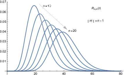
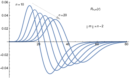
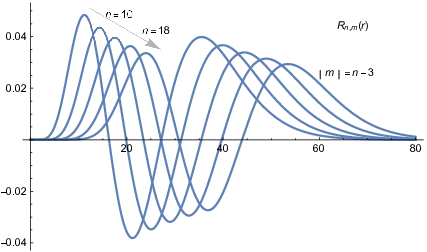
The characteristic order of the magnitude is . This is a very large quantity which is beyond the applicability domain of the simple model of Eq.(1). However, if and , then , and that revives the envelope-function assumptions. If so,
| (7) |
Note, that although the states and are degenerate, they belong to different valleys. These states have positive energies, but they are discrete and localized. This is an unusual, but not forbidden situation. In fact, the motion in the coordinate space automatically changes the relation of electron momentum and the local valley minimum; that blocks electron relocation and localizes the electron states.
Another remark concerns the spectrum discreetness. As far as energies are proportional to the rational expression from numbers and , the spectrum covers all positive energies .
Thus, essentially different electron spectrum shows the important influence of the valley center coordinate dependence on the electron states.
Optical transitions
Let us illuminate the system by some normally directed circular-polarized light which is resonant with respect to some interlevel distance. To determine the interlevel transition probability it is necessary to calculate the matrix elements of operator , where is the velocity operator corresponding to the Hamiltonian Eq.(1), and is the electromagnetic wave polarization vector.
The matrix elements are expressed via the integrals of the radial functions and, for circular polarization , they are given
| (8) |
Eq.(Optical transitions), together with the wave functions Eq.(Coulomb-like states), allows easy to calculate the oscillator strengths for different optical transitions.
Taking into account that the light causes dipole transitions, we have for, say, . If . the transitions occur between localized states in the valley . At the same time another valley will stay inactive. In other words, in dependence on the polarization sign (i.e., on sign of ), the selected valley will be active or not with respect to transitions between discrete levels.
Thus, we can selectively excite electrons in the valleys or . This property unifies the considered system with non-deformed dichalcogenides. However, in the deformed crystal the excitation touches the localized states, instead of 2D extended states in non-deformed dichalcogenides.
Note, that the transitions in non-active valley occur also, but they have no resonant nature; this means much lower absorption at frequency corresponding to discrete states.
Generalizations
The case .
The obtained results can be simply generalized. First, one can consider another configuration of vector , when . In this case represents a potential field, , and can be excluded from the wave function by the gauge transformation. Thus, does not influence electron states.
Two-bands narrow-gap model.
Another generalization concerns the model. In fact, the considered basic materials have relatively close conduction (c) and valence (v) energy bands. The previous consideration is valid for an electron state close to the conduction band bottom. To extend the model one should base on the minimal two-band model di xiao; falko. Taking into account the dependence of vector on , the Hamiltonian of this model becomes
Here is the interband velocity, is the gap between c- and v-bands. The eigenfunction of Eq.(Two-bands narrow-gap model.) is the two-component spinor Eliminating from the system of equations , we find:
| (12) |
We have used relation . For the case, , Eq.(12), after separating the angular variable (), is transformed into
| (13) |
Comparing Eq.(13) with Eq.(4) we obtain the expression for the spectrum in the two-band case:
| (14) |
or expanding with respect to large and :
| (15) |
Gapped graphene cone
Conic graphene ripples were realized in bouchiat-bouchiat1 and bouchiat-bouchiat2. From the theoretical point of view, a disadvantage of planar deformed gapped graphene is a strong deformation of external graphene parts. Conic graphene is a system where the in-plane deformation vanishes. Such system is similar to a inextensible sheet of paper rolled into a cone. In fact, this system is equivalent to planar graphene. Here we consider the conic gapped graphene within the single-band approximation.
To fulfill the adiabaticity requirement one can cut sector from a graphene disk with radius , then connect the edges of the cut. As a result, we obtain a cone where the crystal structure is continuously repeated through the cut (see Fig.(16). The cone height is , the base radius is .


Mathematically, in the envelope approximation, electrons in gapped graphene on the surface can be described by the Schrödinger equation in spherical coordinates
| (16) |
Here is the half-angle at the cone apex, is the distance to the apex. In the cone shown in Fig.(16) . After the separation of angle we come to
Summary
In conclusion, we have found the electron states in a planar deformed multivalley 2D system. Unexpectedly, the influence of the adiabatic deformation turned to be strong. One can consider this new interaction as a topological one. The characteristic energy of this interaction is based on quantity . This quantity has the value of the order of several , and it exceeds the deformation potential, which reaches such value at an extreme linear deformation only. Also, this topological interaction exceeds the characteristic geometric potential (which entirely vanishes for planar deformation, but can be nonzero for the space deformation of a plane of the system). Obviously, there is a lot of different other deformation kinds of 2D systems. However, our finding shows the important role of the vector rotation, considered in the present paper.
Acknowledgements
This work has been supported by RFBR grant No 20-02-00622.
References
- (1) R.C.T. da Costa, Phys.Rev.A 23, 1982 (1981).
- (2) N. Ogawa, K. Fujii, and A. Kobushukin, Prog.Theor.Phys. 83, 894 (1990).
- (3) L.I. Magarill, D.A. Romanov, and A.V. Chaplik, JETP 64, No 4, 460 (1998) [[Zh.Eksp.Teor.Fiz. 86, No 4, 771 (1998].
- (4) M.V. Entin and L.I. Magarill, Phys.Rev B 64, 085330 (2001).
- (5) L.I. Magarill and M.V. Entin, JETP 96, No. 4, 2003, 766 (2003) [Zh.Eksp.Teor.Fiz. 123, No. 4, 867 (2003)].
- (6) A.V. Chaplik and M.V. Entin, Soviet Phys. JETP 34, 1335 (1972) [Zh.Eksp.Teor.Fiz. 61, 2496 (1971)].
- (7) X.L. Yang, S.H. Guo, F.T. Chan, K.W. Wong, W.Y. Ching, Phys.Rev.A 43, 1186 (1990).
- (8) Di Xiao, Gui-Bin Liu, Wanxiang Feng, Xiaodong Xu, and Wang Yao, Phys.Rev.Lett. 108, 196802 (2012).
- (9) A. Kormanyos, G. Burkard, M. Gmitra, J. Fabian, V. Zolyomi, N.D. Drummond, and V. Falko, 2D Materials 2, 022001 (2015).
- (10) Antoine Reserbat-Plantey, Dipankar Kalita, Laurence Ferlazzo, Sandrine Autier-Laurent, Katsuyoshi Komatsu, Chuan Li, Raphael Weil, Zheng Han, Sandrine Autier-Laurent, Arnaud Ralko, Laetitia Marty, Sophie Gueron, Nedjma Bendiab, Helene Bouchiat, and Vincent Bouchiat. arXiv:1404.5783v2[cond-mat.mes-hall]
- (11) Antoine Reserbat-Plantey, Dipankar Kalita, Zheng Han, Laurence Ferlazzo, Sandrine Autier-Laurent, Katsuyoshi Komatsu, Chuan Li, Raphael Weil, Arnaud Ralko, Laetitia Marty, Sophie Gueron, Nedjma Bendiab, Helene Bouchiat, and Vincent Bouchiat, Nano Lett. 14, No 9, 5044 (2014).