Theoretical analysis of thermal boundary conductance of MoS2-SiO2 and WS2-SiO2 interface
Abstract
Understanding the physical processes involved in interfacial heat transfer is critical for the interpretation of thermometric measurements and the optimization of heat dissipation in nanoelectronic devices that are based on transition metal dichalcogenide (TMD) semiconductors. We model the phononic and electronic contributions to the thermal boundary conductance (TBC) variability for the MoS2-SiO2 and WS2-SiO2 interface. A phenomenological theory to model diffuse phonon transport at disordered interfaces is introduced and yields and MW/K/m2 at 300 K for the MoS2-SiO2 and WS2-SiO2 interface, respectively. We compare its predictions to those of the coherent phonon model and find that the former fits the MoS2-SiO2 data from experiments and simulations significantly better. Our analysis suggests that heat dissipation at the TMD-SiO2 interface is dominated by phonons scattered diffusely by the rough interface although the electronic TBC contribution can be significant even at low electron densities ( cm-2) and may explain some of the variation in the experimental TBC data from the literature. The physical insights from our study can be useful for the development of thermally aware designs in TMD-based nanoelectronics.
I Introduction
Atomically thin two-dimensional (2D) transition metal dichalcogenide (TMD) semiconductors such as MoS2 and WS2 hold great potential for the development of next-generation electronic devices (Li et al. 2015; Lembke et al. 2015). At the nanoscale, high power densities in these devices require efficient thermal management crucial for optimal device performance, with the thermal boundary conductance (TBC) of the 2D crystal-substrate interface playing a key role in the dissipation of excess Joule heat (Pop 2010; Ong and Bae 2019). Therefore, clearer insights into the role of the different physical mechanisms underlying the TBC of the TMD-substrate interface may lead to superior thermally aware TMD-based nanoelectronic device designs.
One widely studied mechanism is the van der Waals coupling between the phonons of the 2D crystal and its substrate which is believed to be the dominant component in the overall TBC (Ong and Bae 2019). The phononic TBC () has been estimated using molecular dynamics (MD) simulations (Ong et al. 2018; Suryavanshi et al. 2019), elasticity theory (Persson et al. 2011; Ong et al. 2016; Ong 2017) and density functional theory-based models (Correa et al. 2017). Another mechanism of heat dissipation is through the inelastic scattering of electrons in the 2D crystal by dipoles in the dielectric substrate, a phenomenon known widely as “remote phonon (RP) scattering” or “surface optical phonon scattering” (Hess and Vogl 1979; Fischetti et al. 2001; Konar et al. 2010; Zou et al. 2010). This inelastic scattering mechanism, which plays an important role in limiting the electron mobility in TMDs (Yu et al. 2014; Yu et al. 2016), also underlies the electronic TBC () and depends strongly on the electron or hole density. Although it is predicted to be insubstantial for heat dissipation in graphene (Ong et al. 2013; Koh et al. 2016), the contribution from RP scattering may be significant and comparable to the phononic TBC for MoS2 and WS2 (Ong et al. 2020).
Nonetheless, even though the phononic TBC has been studied using various theoretical methods, it is useful to have a model that relates to the fundamental elastic properties of the 2D crystal and its substrate while accounting for quantum statistics at low temperatures. One such theory that is based on coherent flexural phonons (Persson et al. 2011) and developed in Ref. (Ong et al. 2016) yields relatively accurate values for the graphene-SiO2 interface (Ong et al. 2016; Ong 2017) and also predicts a modest room-temperature phononic TBC of MW/K/m2 for the MoS2-SiO2 interface, in good agreement with earlier published data (Taube et al. 2015) but considerably smaller than later more accurately measured TBC values (Yalon et al. 2017a; Yalon et al. 2017b) in the range of to MW/K/m2. This substantial discrepancy necessitates a relook of the heat dissipation mechanisms at the TMD-substrate substrate.
In our paper, we model the relative contribution of the different physical mechanisms to the overall TBC of the MoS2-SiO2 and WS2-SiO2 interface. Our objective is to understand how these mechanisms (e.g. coherent vs. diffuse phonon transport and the electron density dependence of ) lead to the variability in their TBC. We revisit the phononic TBC problem and introduce a phenomenological diffuse phonon theory that is more suitable for atomically disordered interfaces and allows us to model the effect of disorder on the TBC. To understand its difference to the coherent theory, we compare the TBC predictions from the coherent and diffuse phonon models with data from experiments and MD simulations. We also compare the phononic contribution (coherent or diffuse) to the electronic contribution in the TBC. Finally, we use the combined electronic and phononic BC results () to analyze reported experimental TBC data (Taube et al. 2015; Yalon et al. 2017b; Yalon et al. 2017a; Yasaei et al. 2017) for the MoS2-SiO2 interface and to discuss the possible physics underlying the variability of the TBC data. We also use the combined electronic and phononic BC results to predict the variability of the TBC for the WS2-SiO2 interface. Although the theoretical methods in this paper are used specifically to analyze the TBC variability of the single-layer MoS2-SiO2 and WS2-SiO2 interface, they can also be extended to other 2D crystals (e.g. graphene and other TMDs) and substrates (e.g. Al2O3).
II Theoretical models
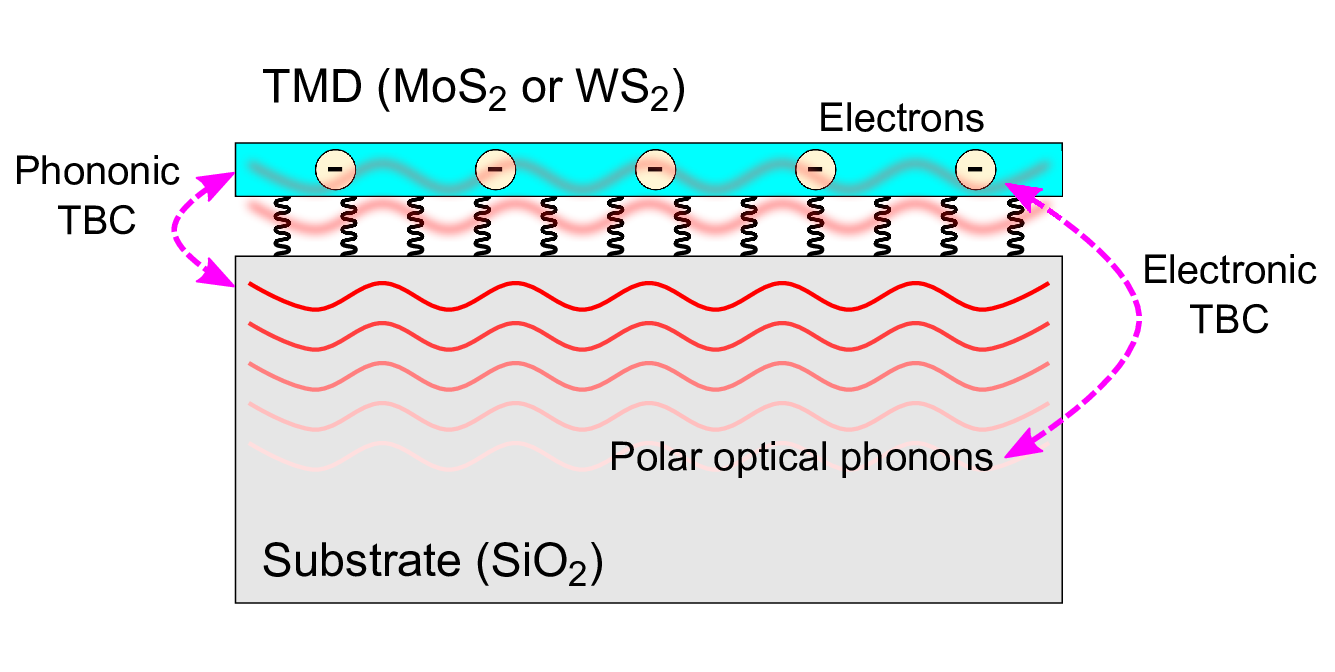
We discuss our theoretical models of the phononic and electronic TBC processes, as depicted in the schematic of the TMD-substrate interface in Fig. 1, in the following subsections. Roughly speaking, we attribute the phononic TBC () to the linear mechanical coupling between the flexural phonons of the TMD sheet and the bulk elastic waves (i.e., acoustic phonons) of the substrate, and the electronic TBC () to the remote scattering of the TMD electrons by the polar optical phonons of the dielectric substrate, also otherwise known as “remote phonon scattering” (Hess and Vogl 1979; Ong et al. 2020). We assume that the two TBC components are independent (i.e., the electron-phonon interaction has no effect on the mechanical coupling between the TMD and the substrate and vice versa) and can be added in parallel.
II.1 Heat dissipation from coherent and diffuse flexural phonon scattering
We adopt a linear elasticity theory-based approach to model the phononic TBC from Ref. (Ong et al. 2016). Although the model is applied to the TMD-SiO2 interface here, it is sufficiently general to be applied to any linear elastic isotropic substrate. The model, which assumes heat dissipation by coherent 2D flexural phonons at a perfectly smooth interface (Persson et al. 2011), is used to derive the following expression for the coherent phononic TBC
| (1) |
where
| (2) |
is the coherent areal transmission function, is the maximum wave vector which we can set as m-1 ( is the unit cell area of the TMD), and is the Bose-Einstein occupation factor at frequency and temperature . The transmission function in Eq. (2) depends on the spring constant at the TMD-substrate interface , the retarded Green’s function for the flexural motion of the TMD monolayer , and the retarded Green’s function for the free surface displacement of the isotropic solid substrate . The value of for the MoS2-SiO2 interface is taken from Ref. (Ong et al. 2016) while its value for the WS2-SiO2 interface is calculated using density functional theory like in Ref. (Ong et al. 2016).
The expressions for and are (Ong et al. 2016)
| (3) |
where and denote the areal mass density and the bending stiffness of the uncoupled 2D crystal, respectively, and
| (4) |
where
| (5a) | ||||
| (5b) | ||||
| (5c) | ||||
and , and are the longitudinal and transverse speed of sound, and the voluminal mass density of the substrate, respectively. In Eq. (4), represents the Heaviside function, and rad/s (or meV) and m-3 are respectively the longitudinal Debye frequency and number density (Goodson et al. 1994) of the substrate (amorphous SiO2). As in Ref. (Ong et al. 2016), in Eq. (3) is the frequency-dependent damping coefficient representing the intrinsic damping of the flexural motion, given as where is the ratio of the phonon lifetime to its period at room temperature and is the room temperature ( K). It has been shown (Ong et al. 2016) that it is necessary to include the intrinsic damping of the flexural motion in Eq. (3) to account for the interfacial heat dissipation correctly.
Although the predictions of the coherent flexural phonon model are relatively accurate for graphene (Ong et al. 2016; Ong 2017), its predictions for the MoS2-SiO2 interface are substantially smaller than experimental data (Yalon et al. 2017a; Yalon et al. 2017b), highlighting a possible shortcoming of the model. The theory in Eq. (2) assumes a perfectly smooth interface (Persson et al. 2011) which limits energy transfer to processes that conserve parallel momentum, a restriction that may not apply to the more disordered TMD-substrate interface which can have surface roughness, trapped charged impurities and surface adsorbates (Rhodes et al. 2019). For a highly disordered interface, this assumption can be relaxed and we may assume that each incoming phonon is scattered by the disordered interface without constraints to all available outgoing phonon modes with equal probability like in the diffuse mismatch model (DMM) (Swartz and Pohl 1989). Using this assumption, we apply the DMM approximation to modify Eq. (1) by writing the diffuse transmission function between the 2D crystal and the substrate as (Zhang et al. 2018)
| (6) |
where and are the number of available transmitting modes per unit area at frequency in the 2D crystal and substrate, respectively. We stress that Eq. (6) describes a phenomenological model derived from purely kinetic considerations of detailed balance (Swartz and Pohl 1989; Zhang et al. 2018) and ignores the details of the interactions at the interface. The corresponding TBC is
| (7) |

To determine in Eq. (6), we need to count the number of modes in the 2D crystal and the substrate that contribute to cross-plane phonon transport at each frequency . This problem is particularly tricky for a single-layer 2D crystal since it has no extended volume in the cross-plane direction as shown in Fig. 2(a). Instead, we estimate in our model phenomenologically by assuming that the interface between the 2D crystal and a substrate consisting of a semi-infinite number of the same 2D material is acoustically transparent, e.g. a single-layer MoS2 (1L-MoS2) on a bulk MoS2 (L-MoS2) substrate, such that the transmission function between the two materials is equal to the number of transmitting modes in the single-layer 2D crystal. To do this, we make the replacement and in Eq. (2), where
| (8) |
is the surface response function of a semi-infinite 2D layered substrate (Ong et al.), with
for , and is the interlayer spring constant in the substrate. Hence, we obtain the expression analogous to Eq. (2), i.e.,
| (9) |
which can be evaluated numerically. The set up of the calculation for for a single-layer TMD (1L-TMD) is shown in Fig. 2(b). In the case of SiO2 as shown in Fig. 2(c), we estimate the number of modes per unit area in an isotropic elastic substrate as
| (10) |
Since for , we have and Eq. (7) becomes
| (11) |
which depends on the substrate through its longitudinal Debye frequency and the 2D crystal though . The expression in Eq. (11) suggests that in the diffuse limit, the phononic TBC for a particular 2D crystal can be maximized only through which depends on . Hence, the phononic TBC would be high for hard insulators such as diamond and sapphire for which and m/s, respectively (Swartz and Pohl 1989).
| TMD | WS2 | MoS2 |
|---|---|---|
| ( Nm-3) | ||
| (eV) | (Lai et al. 2016) | (Lai et al. 2016) |
| ( kgm-2) | ||
| (Ong et al. 2016) | ||
| (kgm-3) | (Persson et al. 2011) | |
| (ms-1) | (Persson et al. 2011) | |
| (ms-1) | (Persson et al. 2011) | |
| (meV) | ||
| ( Nm-3) | (Liang et al. 2017) | (Liang et al. 2017) |
II.2 Heat dissipation by remote phonon scattering
To model the electronic TBC , we use the theory developed in Ref. (Ong et al. 2020). The expression for is written as a 2D integral that can be evaluated numerically, i.e.,
| (12) |
where m-1 is the cutoff wave vector like in Eq. (2), is the frequency of the phonon, is the TMD-substrate gap size, is the chemical potential, and
| (13) |
In Eq. (12), is the electron polarizability (Ong et al. 2020) while the screening function is given by (Ong and Fischetti 2012a)
| (14) |
where and are the electron charge and the permittivity of vacuum, respectively. In Eq. (13), the expressions for , , and are given by , , and where and are the transverse optical phonon frequencies associated with the bulk polar optical phonons of the substrate.
We use the simulation parameters from Table 2 for our calculations. The longitudinal optical (LO) phonon frequencies and are determined from the zeros of while the surface optical (SO) phonon frequencies and are determined from solving (Konar et al. 2010).
| Substrate | WS2 | MoS2 |
|---|---|---|
| (Å) | 3.0 (Ong et al. 2020) | |
| 2 | ||
| 2 | ||
| 2.50 | ||
| 3.05 | ||
| 3.90 | ||
| (meV) | 55.60 | |
| (meV) | 138.10 | |
| (meV) | 60.99 | |
| (meV) | 148.97 | |
III Numerical results and discussion
III.1 Comparison of coherent and diffuse phononic TBC
It is intuitively expected that disorder in the interface leads to higher thermal resistance because of increased phonon scattering (Hopkins 2013). However, the presence of interfacial disorder can enlarge the scattering phase space and possibly improve interfacial thermal transport by allowing energy transfer to proceed through scattering pathways that do not conserve parallel momentum (Tian et al. 2012). This difference in scattering is manifested in the transmission spectra and from Eqs. (2) and (6) in Fig. 3(a) which shows a marked difference in the transmission spectra for the MoS2-SiO2 interface, especially at low frequencies ( meV) where is substantially higher than . The sharp drop in the transmission spectra observed at meV is due to the frequency cutoff at the longitudinal Debye frequency of the substrate.
To understand the implications of the difference in the transmission spectra between the ordered and disordered TMD-substrate interface, we compare and of Eqs . (1) and (7) from to K, using the parameters in Table 1, for the WS2-SiO2 and MoS2-SiO2 interface in Fig. 3(b). For the MoS2-SiO2 interface at K, we obtain MW/K/m2, which is significantly larger than MW/K/m2 and more comparable to the value of MW/K/m2 at K in Ref. (Yalon et al. 2017a), – MW/K/m2 at K in Ref. (Yasaei et al. 2017), MW/K/m2 at K in Ref. (Guo et al. 2019) and MW/K/m2 at K in Ref. (Yu et al. 2020). This suggests that the MoS2-SiO2 interface is disordered, possibly connected to the absence of long-range order in a-SiO2 and chemical inhomogeneity of its surface (Rhodes et al. 2019), and that its thermal transport properties are better described by the diffuse phonon model. The larger for the MoS2-SiO2 interface is also closer to classical MD simulation results ( MW/K/m2 in Ref. (Yasaei et al. 2017), – MW/K/m2 in Ref. (Farahani et al. 2018) and MW/K/m2 in Ref. (Suryavanshi et al. 2019)). For the WS2-SiO2 interface at 300 K, we also find that MW/K/m2 is significantly larger than MW/K/m2. The good agreement of with experimentally derived values for the MoS2-SiO2 interface suggests that the real TBC value for the WS2-SiO2 interface is probably closer to the predicted MW/K/m2. We also note that the and values for the WS2-SiO2 and MoS2-SiO2 interface are comparable because of their similar elasticity parameters (, and ).

III.2 Interpretation of experimental data for MoS2-SiO2 interface
We combine the results for , and to analyze the experimental TBC data () for the MoS2-SiO2 interface from Yalon et al. (Yalon et al. 2017a). As mentioned earlier, we assume that the phononic and electronic TBC components are independent and can be added in parallel, and that the electronic TBC is unaffected by the disorder at the TMD-substrate interface. In Fig. 4, we plot , , (coherent phononic and electronic) and (diffuse phononic and electronic) at different values of the electron density from to cm-2 in steps of cm-2 as a function of temperature and compare them to the data.
At cm-2, there is no electronic contribution to the overall TBC and the theoretical TBC values are given by or which we can treat as the baseline TBC. We find that the values are significantly higher than and in much closer agreement with over the temperature range of 311 to 558 K. This suggests that the diffuse phonon model captures the essential physics of heat dissipation at the MoS2-SiO2 interface and that electronic contribution to the TBC is not reflected in the data.
Nonetheless, we explore the effects of the electronic contribution to the total TBC which can be significant. Figure 4 shows that data can also be fitted by at cm-2, i.e., the discrepancies between the experimental TBC data and the predicted coherent phononic TBC ones can be eliminated by adding the contribution from the remote phonon scattering of TMD electrons. Although the predictions for at the relatively low electron density of cm-2 seem to fit the data slightly better at higher temperatures that the predictions do, the error bars in the data are too large for us to exclude or as the phononic component of the total TBC. Nonetheless, we favor as the phononic component because its predicted values are closer to classical MD simulation results (Yasaei et al. 2017; Farahani et al. 2018; Suryavanshi et al. 2019) which have no electronic contribution.
The substantial spread in the predictions in the to cm-2 range may also explain the variation in the experimental TBC values for the MoS2-SiO2 interface. It has been reported that the intrinsic doping of single-layer MoS2 can reach up to cm-2 on SiO2 substrates (Baugher et al. 2013; Mak et al. 2013) although not all the electrons are delocalized (Qiu et al. 2013). In samples grown by chemical vapor deposition, a maximum electron density of cm-2 can be reached using an applied gate voltage (Smithe et al. 2017). Nonetheless, we limit our analysis in the following discussion to a conservative cm-2 range as there has not been any systematic attempt to measure how the TBC varies with . As increases from to cm-2, the theoretical TBC at K increases from to MW/K/m2, producing a spread comparable to the TBC variation ( to MW/K/m2) obtained at K in Ref. (Yasaei et al. 2017). This suggests that the spread in TBC values may be caused by the variability in the electron density due to intrinsic doping in MoS2 (Leong et al. 2015) which is often -doped as a result of sulfur atom vacancies (Qiu et al. 2013). It also implies that it should be possible to increase the TBC of the MoS2-SiO2 interface by doping the MoS2 through the introduction of dopants (Kiriya et al. 2014; Rastogi et al. 2014) or the use of a metal gate electrode (as in a field-effect transistor) to modulate the electron density. In addition to the change in the TBC as increases, another striking feature is the change in the temperature dependence of the TBC.

III.3 Phononic and electronic TBC for WS2-SiO2 interface
We also present the simulated electronic and phononic TBC for the WS2-SiO2 interface in Fig. 5 in which we plot , , (coherent phononic and electronic) and (diffuse phononic and electronic) at different values of the electron density from to cm-2 in steps of cm-2 as a function of temperature. Unlike Fig. 4, no comparison with experimental data is made because no such data is available for the WS2-SiO2 interface. Nevertheless, the data in Fig. 5 can be useful for comparison with future experimental TBC measurements of the WS2-SiO2 interface and understanding its TBC variability.
We observe similar trends in Fig. 5 to the data in Fig. 4. At 300 K, as increases from to cm-2, increases from to MW/K/m2 while increases from to MW/K/m2. We note that the , and data for the WS2-SiO2 interface are comparable but smaller than their corresponding values for the MoS2-SiO2 interface in Fig. 4. The large change in the and data with respect to means that a change in electron density, from either intrinsic doping or an applied gate voltage, can also lead to a significant detectable change in the measured TBC as with the MoS2-SiO2 interface.

IV Summary and conclusion
In this work, we analyze the theoretical phononic and electronic TBC of the WS2-SiO2 and MoS2-SiO2 interface. To describe the phononic TBC contribution for the disordered TMD-substrate interface, we introduce a diffuse phonon model. We compare the coherent and diffuse phonon models for the WS2-SiO2 and MoS2-SiO2 interface, and find that the diffuse phonon model yields significantly higher TBC values that fit the TBC data for the MoS2-SiO2 interface from molecular dynamics simulations and thermometric experiments better, implying that the TMD-substrate interfaces are disordered. Our analysis of the experimental TBC data from Ref. (Yalon et al. 2017a) for the MoS2-SiO2 interface indicates that the overall TBC is dominated by diffuse phonon transport although the electronic contribution from remote phonon scattering can be significant even at low electron densities and becomes comparable to the phononic contribution at higher electron densities. The simulated phononic and electronic TBC data for the WS2-SiO2 interface also indicate that the electronic contribution to its TBC is also significant. Our results show that the spread in experimental TBC values of the MoS2-SiO2 interface can possibly be explained by the variability in intrinsic doping which affects the electronic TBC.
Acknowledgements.
We gratefully acknowledge support from the Science and Engineering Research Council through grant (152-70-00017) and use of computing resources at the A*STAR Computational Resource Centre and National Supercomputer Centre, Singapore. We also thank Eilam Yalon (Technion, Israel Institute of Technology) for sharing the experimental data from Ref. (Yalon et al. 2017a) with us.References
- Li et al. (2015) X. Li, L. Yang, M. Si, S. Li, M. Huang, P. Ye, and Y. Wu, Advanced Materials 27, 1547 (2015).
- Lembke et al. (2015) D. Lembke, S. Bertolazzi, and A. Kis, Accounts of Chemical Research 48, 100 (2015).
- Pop (2010) E. Pop, Nano Research 3, 147 (2010).
- Ong and Bae (2019) Z.-Y. Ong and M.-H. Bae, 2D Materials 6, 32005 (2019).
- Ong et al. (2018) Z.-Y. Ong, B. Qiu, S. Xu, X. Ruan, and E. Pop, J. Appl. Phys. 123, 115107 (2018).
- Suryavanshi et al. (2019) S. V. Suryavanshi, A. J. Gabourie, A. Barati Farimani, and E. Pop, J. Appl. Phys. 126, 55107 (2019).
- Persson et al. (2011) B. N. J. Persson, A. I. Volokitin, and H. Ueba, J. Phys.: Condens. Matter 23, 45009 (2011).
- Ong et al. (2016) Z.-Y. Ong, Y. Cai, and G. Zhang, Phys. Rev. B 94, 165427 (2016).
- Ong (2017) Z.-Y. Ong, Phys. Rev. B 95, 155309 (2017).
- Correa et al. (2017) G. C. Correa, C. J. Foss, and Z. Aksamija, Nanotechnology 28, 135402 (2017).
- Hess and Vogl (1979) K. Hess and P. Vogl, Solid State Communications 30, 797 (1979).
- Fischetti et al. (2001) M. V. Fischetti, D. A. Neumayer, and E. A. Cartier, J. Appl. Phys. 90, 4587 (2001).
- Konar et al. (2010) A. Konar, T. Fang, and D. Jena, Phys. Rev. B 82, 115452 (2010).
- Zou et al. (2010) K. Zou, X. Hong, D. Keefer, and J. Zhu, Phys. Rev. Lett. 105, 126601 (2010).
- Yu et al. (2014) Z. Yu, Y. Pan, Y. Shen, Z. Wang, Z. Y. Ong, T. Xu, R. Xin, L. Pan, B. Wang, L. Sun, J. Wang, G. Zhang, Y. W. Zhang, Y. Shi, and X. Wang, Nature Communications 5, 5290 (2014).
- Yu et al. (2016) Z. Yu, Z.-Y. Ong, Y. Pan, Y. Cui, R. Xin, Y. Shi, B. Wang, Y. Wu, T. Chen, Y.-W. Zhang, G. Zhang, and X. Wang, Advanced Materials 28, 547 (2016).
- Ong et al. (2013) Z.-Y. Ong, M. V. Fischetti, A. Y. Serov, and E. Pop, Phys. Rev. B 87, 195404 (2013).
- Koh et al. (2016) Y. K. Koh, A. S. Lyons, M. H. Bae, B. Huang, V. E. Dorgan, D. G. Cahill, and E. Pop, Nano Lett. 16, 6014 (2016), arXiv:1603.00358 .
- Ong et al. (2020) Z.-Y. Ong, G. Zhang, L. Cao, and Y.-W. Zhang, Phys. Rev. Research 2, 033470 (2020).
- Taube et al. (2015) A. Taube, J. Judek, A. Lapinska, and M. Zdrojek, ACS Appl. Mater. Interfaces 7, 5061 (2015).
- Yalon et al. (2017a) E. Yalon, O. B. Aslan, K. K. H. Smithe, C. J. McClellan, S. V. Suryavanshi, F. Xiong, A. Sood, C. M. Neumann, X. Xu, K. E. Goodson, T. F. Heinz, and E. Pop, ACS Appl. Mater. Interfaces 9, 43013 (2017a).
- Yalon et al. (2017b) E. Yalon, C. J. McClellan, K. K. H. Smithe, M. Munoz Rojo, R. L. Xu, S. V. Suryavanshi, A. J. Gabourie, C. M. Neumann, F. Xiong, A. B. Farimani, and E. Pop, Nano Lett. 17, 3429 (2017b).
- Yasaei et al. (2017) P. Yasaei, C. J. Foss, K. Karis, A. Behranginia, A. I. El-Ghandour, A. Fathizadeh, J. Olivares, A. K. Majee, C. D. Foster, F. Khalili-Araghi, Z. Aksamija, and A. Salehi-Khojin, Advanced Materials Interfaces 4, 1700334 (2017).
- Goodson et al. (1994) K. E. Goodson, M. I. Flik, L. T. Su, and D. A. Antoniadis, J. Heat Transfer 116, 317 (1994).
- Rhodes et al. (2019) D. Rhodes, S. H. Chae, R. Ribeiro-Palau, and J. Hone, Nature Materials 18, 541 (2019).
- Swartz and Pohl (1989) E. T. Swartz and R. O. Pohl, Rev. Mod. Phys. 61, 605 (1989).
- Zhang et al. (2018) J. Zhang, C. A. Polanco, and A. W. Ghosh, J. Heat Transfer 140, 092405 (2018), arXiv:1612.04807 .
- (28) Z.-Y. Ong, Y. Cai, G. Zhang, and Y.-W. Zhang, Submitted .
- Lai et al. (2016) K. Lai, W. B. Zhang, F. Zhou, F. Zeng, and B. Y. Tang, J. Phys. D: Appl. Phys. 49, 185301 (2016).
- Liang et al. (2017) L. Liang, J. Zhang, B. G. Sumpter, Q. H. Tan, P. H. Tan, and V. Meunier, ACS Nano 11, 11777 (2017).
- Ong and Fischetti (2012a) Z.-Y. Ong and M. V. Fischetti, Phys. Rev. B 86, 121409 (2012a).
- Jin et al. (2014) Z. Jin, X. Li, J. T. Mullen, and K. W. Kim, Phys. Rev. B 90, 045422 (2014), arXiv:1406.4569 .
- Ong and Fischetti (2012b) Z.-Y. Ong and M. V. Fischetti, Phys. Rev. B 86, 165422 (2012b).
- Hopkins (2013) P. E. Hopkins, ISRN Mechanical Engineering 2013, 682586 (2013).
- Tian et al. (2012) Z. Tian, K. Esfarjani, and G. Chen, Phys. Rev. B 86, 235304 (2012).
- Guo et al. (2019) J. Guo, F. Yang, M. Xia, X. Xu, and B. Li, J. Phys. D: Appl. Phys. 52, 385306 (2019).
- Yu et al. (2020) Y. Yu, T. Minhaj, L. Huang, Y. Yu, and L. Cao, Physical Review Applied 13, 034059 (2020).
- Farahani et al. (2018) H. Farahani, A. Rajabpour, M. Khanaki, and A. Reyhani, Computational Materials Science 142, 1 (2018).
- Baugher et al. (2013) B. W. Baugher, H. O. Churchill, Y. Yang, and P. Jarillo-Herrero, Nano Lett. 13, 4212 (2013).
- Mak et al. (2013) K. F. Mak, K. He, C. Lee, G. H. Lee, J. Hone, T. F. Heinz, and J. Shan, Nature Materials 12, 207 (2013).
- Qiu et al. (2013) H. Qiu, T. Xu, Z. Wang, W. Ren, H. Nan, Z. Ni, Q. Chen, S. Yuan, F. Miao, F. Song, G. Long, Y. Shi, L. Sun, J. Wang, and X. Wang, Nature Communications 4, 2642 (2013).
- Smithe et al. (2017) K. K. Smithe, C. D. English, S. V. Suryavanshi, and E. Pop, 2D Materials 4, 011009 (2017).
- Leong et al. (2015) W. S. Leong, Y. Li, X. Luo, C. T. Nai, S. Y. Quek, and J. T. Thong, Nanoscale 7, 10823 (2015).
- Kiriya et al. (2014) D. Kiriya, M. Tosun, P. Zhao, J. S. Kang, and A. Javey, Journal of the American Chemical Society 136, 7853 (2014).
- Rastogi et al. (2014) P. Rastogi, S. Kumar, S. Bhowmick, A. Agarwal, and Y. S. Chauhan, J. Phys. Chem. C 118, 30309 (2014).