Transport in helical Luttinger liquids in the fractional quantum Hall regime
I abstract
Domain walls in fractional quantum Hall ferromagnets are gapless helical one-dimensional channels formed at the boundaries of topologically distinct quantum Hall (QH) liquids. Naïvely, these helical domain walls (hDWs) constitute two counter-propagating chiral states with opposite spins. Coupled to an s-wave superconductor, helical channels are expected to lead to topological superconductivity with high order non-Abelian excitations Lindner2012; Clarke2012; Alicea2016. Here we investigate transport properties of hDWs in the fractional QH regime. Experimentally we found that current carried by hDWs is substantially smaller than the prediction of the naïve model. Luttinger liquid theory of the system reveals redistribution of currents between quasiparticle charge, spin and neutral modes, and predicts the reduction of the hDW current. Inclusion of spin-non-conserving tunneling processes reconciles theory with experiment. The theory confirms emergence of spin modes required for the formation of fractional topological superconductivity.
II introduction
Gapless chiral edge states, a hallmark of the quantum Hall effect (QHE), are formed at the boundaries of the two-dimensional (2D) electron liquid. These states are protected due to their topological properties; their spatial separation suppresses backscattering and insures precise quantization of the Hall conductance over macroscopic distances PerspQHE2007. Symmetry-protected topological systems can support spatially coexisting counter-propagating states. For example, in 2D topological insulators time reversal symmetry insures orthogonality of Kramers doublets Ando2002; Xu2006; Bardarson2008; in graphene the conservation of angular momentum prevents backscattering in the quantum spin Hall effect regime Young2014. Local symmetry protection is not as robust as spatial separation in the QHE and, as a result, hDWs have finite scattering and localization lengths. Helical states can be also engineered by arranging proximity of two counter-propagating chiral states with opposite polarization, e.g. in electron-hole bi-layers Sanchez-Yamagishi2017 or double quantum well structures Ronen2018, where local charge redistribution between two quantum wells creates two counter-propagating chiral states at the boundary of quantum Hall liquids with different filling factors. In the latter system, spatial separation into two quantum wells suppresses the inter-channel scattering, and transport in each chiral channel is found to be ballistic over macroscopic distances.
An intriguing possibility to form helical channels in the interior of a 2D electron gas is to induce a local quantum Hall ferromagnetic transition. In the integer QHE regime, scattering between overlapping chiral edges from different Landau levels is suppressed due to the orthogonality of the wavefunctions, but spin-orbit interaction mixes states with opposite spins and opens a small gap in the helical spectrum Kazakov2016; Kazakov2017; Simion2018. In the fractional quantum Hall effect (FQHE) regime, electrostatically-controlled transition between unpolarized (u) and polarized (p) states results in the formation of a conducting channel at the boundary between u and p regions (filling factor , where is an external magnetic field, is a flux quanta and is electron density). Superficially, transition between u and p states in the bulk can be understood as a crossing of two composite fermion energy states with opposite spin polarization Ronen2018; Jain1989; Kukushkin1999. Within this model, the hDW at the u-p boundary consists of two counter-propagating chiral states with opposite spin and fractionalized charge excitations, and presents an ideal platform to build fractional topological superconductors with parafermionic and Fibonacci excitations Lindner2012; Clarke2012; Vaezi2013; Mong2014; Vaezi2014; Liang2019. Highly correlated state exhibits rich physics beyond an oversimplified model of integer QHE for weakly interacting composite fermions and includes observation of upstream neutral modes Gurman2012; Inoue2014; Rosenblatt2017; Wang2013, short-range upstream charge modes Lafont2019, and a crossover from to charge excitations in shot noise measurements Bid2009. In the bulk, the spin transition at is accompanied by nuclear polarization Kronmueller1998; Kraus2002; Stern2004 indicating spin-flip processes in the 2D gas, a phenomena not seen in bi-layer systems Ronen2018; Cohen2019. Thus, we expect a hDW formed at a boundary between u and p states to be more complex than a simple overlap of two non-interacting chiral modes.
Here we study the electron transport in samples where hDWs of different length are formed by electrostatic gating. Experimentally, in the limit approximately of the edge current is diverted into the hDW, a number drastically different from the 50% prediction for two non-interacting counter-propagating chiral channels. To address this discrepancy theoretically we consider tunneling between Luttinger liquid modes Wen1995 through a hDW in the strong coupling limit Sandler1999; Nayak1999; Moore2002 . We found that in the presence of a strong inter-edge tunneling edge channels in u and p regions populate unequally, both at the boundary of the 2D gas and within the hDW, forming a number of down- and up-stream charge, spin and neutral modes. For spin-conserving tunneling 1/4 of the incoming charge current is diverted into the hDW, while allowing spin-flip processes further reduces hDW current. Indeed, at high bias currents we observe an increase in the current carried by the hDW. This indicates formation of a bottleneck for spin flips due to Overhauser pumping of nuclei and a crossover from spin-non-conserving to spin-conserving transport.

III Experimental Results
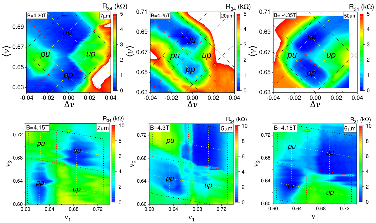
Several devices in a Hall bar geometry with multiple gates have been fabricated in order to study transport through hDWs, Fig. 1 (for heterostructure and fabrication details see Methods). Devices are separated into two regions and ; electron density in these regions can be controlled independently by electrostatic gates. In the IQHE regime when filling factors under gates and differ by one, a single chiral channel is formed along the gates boundary and resistance measured across the boundary is either quantized or zero depending on the sign of the filling factor gradient and direction of (see Supplementary Material). Likewise, a chiral channel is formed when gates boundary separates two different FQHE states.
Fractional QHE states can be understood as integer QHE states for composite fermions in a reduced field, , where is the filling factor for composite fermions JainCFbook2007. Energy separation between composite fermions levels depends on the competition between charging energy and Zeeman energy , and the two lowest energy levels with opposite spins 0-down and 1-up cross at finite due to different field dependencies. When level crossing occurs within the plateau ( for composite fermions), the energy gap for quasiparticle excitations vanishes providing mechanism for charge backscattering and, hence, at resistance of the 2D gas is no longer zero. In our devices it is possible to control by electrostatic gating, and a small peak within the 2/3 plateau in Fig. 1b is a quantum Hall ferromagnetic transition between polarized (p) and unpolarized (u) regions.
Independent control of filling factors and under G1 and G2 divides the 2/3 region into four quadrants uu, pp, up and pu, where the first letter corresponds to polarization of the state under G1 and the second corresponds to polarization under G2. Within the Landauer-Büttiker formalism Beenakker1990; Brey1994 resistance should be zero for all combinations of polarizations under the gates since quantum numbers for both u and p states (here is the Klitzing’s constant). Experimentally is found to be vanishingly small in uu and pp quadrants, consistent with a single topological state being extended over the whole device. in up and pu quadrants indicates backscattering between edge channels and, which, combined with zero longitudinal resistance under G1 and G2, means formation of a conducting channel along the gates boundary. Unlike resistance measured across chiral channels formed, e.g., between and FQHE states (see Supplementary Material), resistance measured across the boundary of u and p quantum liquids at shows almost no dependence on the direction of the external magnetic field and density gradient, consistent with the formation of a helical domain wall Wu2018.

Protection of helical states from backscattering and localization is weaker than for spatially separated chiral edge states, and conduction of hDWs is length dependent. In Fig. 2 a fraction of the external current that flows through the hDW, , is plotted as a function of hDW length . is found to decrease exponentially with , , with a characteristic length m. The value of corresponds to the transport through a ballistic hDW in the absence of localization. Within a simplified model of edge states consisting of equally populated chiral modes and no interaction between chiral channels with opposite spin polarization (Fig. 2a), one expects (marked by a blue arrow in Fig. 2c), an order of magnitude larger than the experimentally observed value (marked by a green arrow). Note that transport through helical modes formed in double quantum well structures are well described by this simple model of weakly interacting chiral states Ronen2018.
IV Theory
An isolated hDW at a boundary of p and u phases was studied in Refs. Wu2018; Liang2019, where disk and torus geometry were employed to avoid physical edges of the sample and coupling of domain wall modes to these edges. Analytical model and numerical results indicate an existence of modes with opposite velocities and spins within the hDW region, a prerequisite for generating topological superconductivity. No neutral or spin modes appear within the K-matrix Luttinger liquid approach Wen1995 in these isolated hDW models. Inclusion of a superconducting pairing term into the hDW Hamiltonian leads to the 6-fold degeneracy of the ground state within a range of parameters, a signature of low energy parafermionic excitations.
To calculate scattering of edge modes at a sample boundary by a hDW we need to move beyond an isolated hDW model. Here we consider tunneling of fractional QH edge states through the hDW in the strong coupling limit. The presence of the hDW imposes boundary conditions on the incoming and propagating modes and affects the population of charge and spin modes along the edges of the u phase and charge and neutral modes along the edges of the p phase. In terms of the separated charged and neutral modes and , the Luttinger liquid action for hierarchical edge states for the p phase reads
| (1) |
where and are velocities of charge and neutral modes, correspondingly. The neutral mode density measures the difference in the occupation of the first two composite fermion -levels. The u phase is described by a similar action, in which the neutral -mode becomes the spin -mode that determines a spin current in the u phase.
In the presence of voltage , change in the mode due to charge injection is characterized by an average induced current . Tunneling between p and u phases carried by electrons with the same spin can be described in terms of quasiparticles by the tunnel Hamiltonian
| (2) |
Mapping of an edge-hDW-edge structure onto one dimensional bosonic modes is shown schematically in Fig. 3a. In general, hDW and each region outside of the hDW may contain up to eight bosonic modes , where , and the superscript {} indicates projection of the velocity on the -axis. However, chirality of edge channels reduces the number of bosonic modes to four. Therefore, it is convenient to consider two charge modes and and two spin/neutral modes and .
In the strong coupling limit charge, neutral and spin currents can be found by imposing the following boundary conditions on bosonic fields right outside of the hDW :
| (3) |
which connect all incoming modes at the right side and outgoing modes at the left side of the equation. Details of calculation, including the account of scattering between p-modes in the polarized region, is presented in Supplementary Materials. The solution for charge fields (Eq. 3) is shown schematically in Fig. 3(b,c) where we assume a unit current incident on the hDW, this current corresponds to in Fig. 2b. There are two quasiparticle bosonic modes along the edges on both p and u sides which we refer to as and . An incoming charge current is divided between and in a ratio 7:1. 1/7 of the mode is scattered back into the p phase across the hDW, while 6/7 is tunneling into the u phase and splits equally between a downstream and an upstream (along the hDW) modes. The bosonic mode has different spin polarization on p and u sides, it carries downstream 1/8 of the total incoming current in p and 3/8 in u phases. In the absence of spin flips there is no tunneling between and modes. The total current backscattered through the hDW or . This value is three times larger than the experimentally measured and is indicated by a red arrow in Fig. 2c.
In 2D gases formed in GaAs heterostructures spin transition at is accompanied by a dynamic nuclear spin polarization Li2008book. Its main mechanism is the hyperfine coupling of electron and nuclear spins, which for QHE plateaus is usually suppressed due to a large difference between electron and nuclear Zeeman splittings. However, near the u-p phase transition electronic states with spin-up and spin-down are almost degenerate, enabling hyperfine coupling. This spin-flip mechanism can couple -up and -down bosonic modes on two sides of the hDW, as shown schematically in Fig. 3c. Assuming this charge transfer induces forward scattering and reduces the fraction of the total current flowing in the hDW from 1/4 to 1/8, which corresponds to (green arrow in Fig. 2c), we obtain the value in a good agreement with the experimentally observed .
To test the role of spin flips it is possible to pass a large dc current and polarize nuclei in the vicinity of the tri-junction. Saturation of nuclear spin polarization is expected to create a bottleneck for electron spin flips and disable charge transfer between two bosonic modes with opposite polarization. Indeed, application of nA results in approximately 3-fold increase of , as shown in the inset in Fig. 2. A corresponding shift of for the 7 m hDW is shown with a vertical arrow on the main plot. This shift is consistent with the 2.3 times current increase expected for the crossover from spin-flip-dominated to no-spin-flip transport.
V Methods
Devices are fabricated from GaAs/AlGaAs inverted single heterojunction heterostructures with electron gas density cm-2 and mobility cm. Details of heterostructure design can be found in Wan2015, these heterostructures demonstrate efficient electrostatic control of the spin transition at Wu2018. Devices are patterned in a Hall bar geometry using e-beam lithography and wet etching, photograph of a typical sample is shown in Fig. 1. Devices are divided into two regions by semi-transparent gates (10 nm of Ti), the gates are separated from the surface of the wafer and from each other by 50nm of Al2O3 grown by the atomic layer deposition (ALD). Gates boundary is aligned with a m - wide mesa constriction. Ohmic contacts are formed by annealing Ni/Ge/Au 30nm/50nm/100nm at 450∘C for 450 seconds in atmosphere. Measurements are performed in a dilution refrigerator at a base temperature of 20 mK using conventional low frequency lock-in technique with excitation current pA. A 2D electron gas is formed by shining red LED at 4 K.
Acknowledgments
Experimental part of the work is supported by NSF award DMR-1836758 (Y.W. and L.P.R.). Theoretical work is supported by the U.S. Department of Energy, Office of Basic Energy Sciences, Division of Materials Sciences and Engineering under Award DE-SC0010544 (Y.L-G). Heterostructures development and growth is funded in part by the Gordon and Betty Moore Foundation’s EPiQS Initiative, Grant GBMF9615 to L.N.P, and by the NSF MRSEC grant DMR-1420541.
Author contributions
Y.W. L.P.R conceived and performed experiments, V.P. and Y.L.G developed theory, K.W.W, K.B and L.N.P. developed and grew heterostructure materials. Y.W, Y.L.G and L.P.R have written the manuscript.
References
- (1) Netanel H. Lindner, Erez Berg, Gil Refael, and Ady Stern, Fractionalizing Majorana Fermions: Non-Abelian Statistics on the Edges of Abelian Quantum Hall States, Phys. Rev. X 2, 041002 (2012).
- (2) David J. Clarke, Jason Alicea, and Kirill Shtengel, Exotic non-Abelian anyons from conventional fractional quantum Hall states, Nat. Commun. 4, 1348 (2012).
- (3) Jason Alicea and Paul Fendley, Topological Phases with Parafermions: Theory and Blueprints, Annual Review of Condensed Matter Physics 7, 119 (2016).
- (4) Perspectives in Quantum Hall Effects: Novel Quantum Liquids in Low-Dimensional Semiconductor Structures, edited by Sankar Das Sarma and Aron Pinczuk (Wiley-VCH Verlag GmbH, Berlin, 2007).
- (5) Tsuneya Ando and Hidekatsu Suzuura, Presence of Perfectly Conducting Channel in Metallic Carbon Nanotubes, J. Phys. Soc. Japan 71, 2753 (2002).
- (6) Cenke Xu and J. E. Moore, Stability of the quantum spin Hall effect: Effects of interactions, disorder, and Z2 topology, Physical Review B 73, 045322 (2006).
- (7) J H Bardarson, A proof of the Kramers degeneracy of transmission eigenvalues from antisymmetry of the scattering matrix, Journal of Physics A: Mathematical and Theoretical 41, 405203 (2008).
- (8) A F Young et al., Tunable symmetry breaking and helical edge transport in a graphene quantum spin Hall state, Nature 505, 528 (2014).
- (9) Javier D Sanchez-Yamagishi et al., Helical edge states and fractional quantum Hall effect in a graphene electron–hole bilayer, Nat. Nanotechnol. 12, 118 (2017).
- (10) Yuval Ronen et al., Robust integer and fractional helical modes in the quantum Hall effect, Nature Physics 14, 411 (2018).
- (11) Aleksandr Kazakov et al., Electrostatic control of quantum Hall ferromagnetic transition: A step toward reconfigurable network of helical channels, Phys. Rev. B 94, 075309 (2016).
- (12) Aleksandr Kazakov et al., Mesoscopic Transport in Electrostatically Defined Spin-Full Channels in Quantum Hall Ferromagnets, Phys. Rev. Lett. 119, 046803 (2017).
- (13) G. Simion et al., Impurity-generated non-Abelions, Physical Review B 97, 245107 (2018).
- (14) J. K. Jain, Composite Fermion approach for the fractional quantum Hall effect, Physical Review Letters 63, 199 (1989).
- (15) I. V. Kukushkin, K. v. Klitzing, and K. Eberl, Spin Polarization of Composite Fermions: Measurements of the Fermi Energy, Phys. Rev. Lett. 82, 3665 (1999).
- (16) Abolhassan Vaezi, Fractional topological superconductor with fractionalized Majorana fermions, Physical Review B 87, 035132 (2013).
- (17) Roger S. K. Mong et al., Universal Topological Quantum Computation from a Superconductor-Abelian Quantum Hall Heterostructure, Physical Review X 4, 011036 (2014).
- (18) Abolhassan Vaezi, Superconducting analogue of the parafermion fractional quantum Hall states, Physical Review X 4, 031009 (2014).
- (19) Jingcheng Liang, George Simion, and Yuli Lyanda-Geller, Parafermions, induced edge states, and domain walls in fractional quantum Hall effect spin transitions, Physical Review B 100, 075155 (2019).
- (20) I. Gurman et al., Extracting net current from an upstream neutral mode in the fractional quantum Hall regime, Nature Communications 3, 1289 (2012).
- (21) Hiroyuki Inoue et al., Proliferation of neutral modes in fractional quantum Hall states, Nature Communications 5, 4067 (2014).
- (22) Amir Rosenblatt et al., Transmission of heat modes across a potential barrier, Nature Communications 8, 2251 (2017).
- (23) Jianhui Wang, Yigal Meir, and Yuval Gefen, Edge reconstruction in the =2/3 fractional quantum Hall state, Physical Review Letters 111, 246803 (2013).
- (24) Fabien Lafont, Amir Rosenblatt, Moty Heiblum, and Vladimir Umansky, Counter-propagating charge transport in the quantum Hall effect regime, Science 363, 54 (2019).
- (25) Aveek Bid et al., Shot noise and charge at the = 2/3 composite fractional quantum Hall state, Physical Review Letters 103, 236802 (2009).
- (26) S. Kronmüller et al., New resistance maxima in the fractional quantum Hall effect regime, Physical review letters 81, 2526 (1998).
- (27) S. Kraus et al., From quantum Hall ferromagnetism to huge longitudinal resistance at the =2/3 fractional quantum Hall state, Physical Review Letters 89, 266801 (2002).
- (28) O. Stern et al., NMR study of the electron spin polarization in the fractional quantum Hall effect of a single quantum well: Spectroscopic evidence for domain formation, Physical Review B 70, 075318 (2004).
- (29) Yonatan Cohen et al., Synthesizing a =2/3 fractional quantum Hall effect edge state from counter-propagating =1 and =1/3 states, Nat. Commun. 10, 1920 (2019).
- (30) Xiao-Gang Wen, Topological orders and edge excitations in fractional quantum Hall states, Adv. Phys. 44, 405 (1995).
- (31) Nancy P. Sandler, Claudio de C. Chamon, and Eduardo Fradkin, Noise measurements and fractional charge in fractional quantum Hall liquids, Phys. Rev. B 59, 12521 (1999).
- (32) Chetan Nayak, Matthew P. A. Fisher, A. W. W. Ludwig, and H. H. Lin, Resonant multilead point-contact tunneling, Physical Review B 59, 15694 (1999).
- (33) Joel E. Moore and Xiao-Gang Wen, Critical points in edge tunneling between generic fractional quantum Hall states, Physical Review B 66, 115305 (2002).
- (34) Jainendra K Jain, Composite fermions (Cambridge University Press, Cambridge, 2007).
- (35) C. W. J. Beenakker, Edge channels for the fractional quantum Hall effect, Phys. Rev. Lett. 64, 216 (1990).
- (36) Luis Brey, Edge states of composite fermions, Phys. Rev. B 50, 11861 (1994).
- (37) Tailung Wu et al., Formation of helical domain walls in the fractional quantum Hall regime as a step toward realization of high-order non-Abelian excitations, Physical Review B 97, 245304 (2018).
- (38) Y. Q. Li and J. H. Smet, in Spin Physics in Semiconductors, edited by Michel I. Dyakonov (Springer Berlin Heidelberg, Berlin, Heidelberg, 2008), pp. 347–388.
- (39) Zhong Wan et al., Induced superconductivity in high-mobility two-dimensional electron gas in gallium arsenide heterostructures, Nature Communications 6, 7426 (2015).
Transport in helical Luttinger liquids in the fractional quantum Hall regime
Ying Wang, Vadim Ponomarenko, Kenneth W. West, Kirk Baldwin, Loren N. Pfeiffer, Yuli Lyanda-Geller, Leonid P. Rokhinson
Supplementary Materials
VI Extended Figures
VII Transport in the presence of a chiral channel
In order to contrast helical and chiral channels we perform measurements of when filling factors and under gates and are different quantum Hall liquids. According to Landauer-Büttiker theory Beenakker1990; Brey1994 for for and for (zero and non-zero values will be switched for ). In Figure S2abc, resistance is plotted over a range of filling factors in IQHE and FQHE regimes. In (d) we plot experimentally measured scaled by ; the values fall within 1% of the expected values.
VIII Modeling of transport through a helical domain wall at
VIII.1 Description of edges of state in terms of bosonic fields and quasiparticle bosonic fields
Luttinger liquid action for hierarchical edge states in terms of bosonic fields of electron operators
| (S1) |
and the charge density is
| (S2) |
where matrix and vector q are given by
| (S3) |
For interaction matrix , we assume that diagonal matrix elements for intra-mode Coulomb interaction is defined by matrix element and off-diagonal matrix elements for inter-mode Coulomb interaction is defined by matrix element ,
| (S4) |
The commutation relation is
| (S5) |
For composite fermion creation operators, we have
| (S6) |
and
| (S7) |
Luttinger liquid action in terms of quasiparticle bosonic fields , defined by is given by
| (S8) |
where
| (S9) |
The two sets of fields are orthogonal:
| (S10) |
The charge mode , and the neutral mode are expressed as follows:
| (S11) |
where in vector form , opetration transposing a row vector into a column vector, and the matrix is given by
| (S12) |
and the following relations hold
| (S13) | |||||
| (S14) |
The neutral mode can be interpreted as a difference in the occupation of edge modes corresponding to the first and second -levels of composite fermions. In the unpolarized phase it coincides with the spin density and we will use spin index instead of .
VIII.2 Description of edges of state in terms of separate charge and neutral/spin modes
In order to discuss the application of voltage to the domain wall system it is convenient to formulate Luttinger liquid action in terms of separate charge and neutral/spin modes. Using matrix defined by Eq. (S12) the transformed matrix , given by Eq. (S3) becomes
| (S15) |
For the transformed matrix ,
| (S16) |
we obtain
| (S17) |
Here we take off-diagonal terms because they are proportional to the difference of velocities of modes and . Then the transformed action is
| (S18) |
The commutation relations for separated charge and neutral (spin) modes are given by
| (S19) | |||||
| (S20) |
To acquire non-zero average charge density and current, density of the charge mode is shifted, . A non-zero average appears due to a charge current injection,
| (S21) |
where V is the applied voltage. Then the average current carried by the edge is
| (S22) |
Shift of the charge mode density is described by an addition to the Luttinger liquid action
| (S23) |
so that .
VIII.3 The Luttinger liquid action in the presence of spin-polarized and spin-unpolarized phases.
The Luttinger liquid action for the edge states at consisting of the two phases, polarized and unpolarized , is given by
where 4x4 matrices
| (S30) |
with matrix defined by Eq. (S3) and
| (S31) |
with matrix is defined by Eq. (S17). For convenience, in order to keep the form of relations for the current as described above for both p and u phases, we reverse the sign of the quasiparticle field , so that .
VIII.4 Tunneling and charge currents
The tunneling between polarized and unpolarized phases for modes carried by composite fermions of the same spin polarization is described by the tunnel Hamiltonian
| (S32) |
where we re-labeled the neutral mode in the unpolarized phase as a spin mode describing the difference in spin density between modes.
VIII.5 Tunneling in the model of zero length hDW
In the strong coupling limit the tunneling current can be found by imposing conditions. A zero-length hDW is the limit of the model of the hDW shown in Fig. 3a of the main text. In order to formulate the boundary conditions, we use quasiparticle modes described by Eqs.(S13,S14) for polarized and unpolarized liquid. Imposing at as a boundary condition that leads to a jump in the tunneling mode and a continuity in the orthogonal, non-tunneling mode, we obtain:
| (S34) | |||
| (S35) |
Using the expressions for quasiparticle modes (S13), we have
| (S36) | |||
| (S37) |
We obtain two more equations defining boundary conditions imposing them for the two modes orthogonal to (S13). These modes are given by
| (S38) | |||
| (S39) |
The boundary conditions for these modes are
| (S40) | |||
| (S41) |
Using explicit expressions for the quasiparticle modes, we obtain that Eqs.( S35,S41) result in the following four equations defning the outgoing fields via incoming fields:
| (S42) |
The current injected into the polarized phase due to the applied voltage shifts only the incoming field
| (S43) |
Using Eq.(S42), we obtain that this change leads to the following changes in outgoing fields:
| (S44) |
The average incoming or outgoing current due to any of the quasiparticle modes (or ) is given by the equation
| (S45) |
where for our choice of signs in action Eq. (VIII.3) charges , is the quasiparticle charge in the polarized phase and is the quasiparticle charge in the unpolarized phase. Describing the currents, we will use indices and for the currents on the polarized and unpolarized side, correspondingly. Upper indices , correspond to the incoming and outgoing currents, lower indices , and correspond to charge, neutral and spin currents. On the polarized side, charge and spin currents coinside; on the unpolarized side, neutral and spin currents coinside. We will assume first that the externally induced incoming charge current comes from the contact with potential to the polarized liquid, and the current flows into the grounded () contact to the unpolarized liquid. Then the incomig current due to (S43) is
| (S46) |
where is the conductance quantum, and the outgoing currents are given by
| (S47) | |||
| (S48) | |||
| (S49) | |||
| (S50) |
where signs of and are changed compared to Eq.(S44) as we transition to counting signs from the right-moving direction, see FigS3.
,
Using the voltage-induced shift of the incoming and outgoing bosonic fields, , , and , given by Eqs (S43), (S44), we can analyze the shift of quasiparticle edge state fields and , that describes the distribution of current over the two quasiparticle modes. The calculation shows that the resulting currents associated with these modes are given by
| (S51) | |||
| (S52) | |||
| (S53) | |||
| (S54) |
where -function at and at is used to describe incoming and outgoing modes in a single equation. We observe that it follows from these equations that tunneling occurs only between and edges,
| (S55) |
while states and flow, correspondingly, in polarized and unpolarized region. Modes and include modes with the same spin up, while modes and carry the opposite spin. This is a consequence of our tunnel Hamiltonian allowing only transmission of like spins. Generalization of the model permitting tunneling with a spin flip, e.g,. induced by interaction with nuclear spins, makes possible some tunneling processes between and modes.
VIII.6 Domain wall of finite length with scattering at the ends
We now combine two point scatterers at points and separated a ballistic domain wall of length . In the experimental setting, these scatterers are the tri-junctions between edge states and the domain wall.
,
Each of the scatterers is described by Eq. (S42). To calculate the transmission through two junctions, it is convenient to present the connection (S42) between 4-vector of incoming modes and 4-vector of outgoing modes in a matrix form:
| (S56) |
where 4x4 matrix is given by
| (S57) |
and 2x2 matrices , are defined by
| (S58) |
| (S59) |
The matrix describes propagation of chiral modes through a single zero-length scatterer, and the matrix describes the reflection of chiral modes. The total 4x4 transfer matrix connects incoming and outgoing modes of two scatterers, via
| (S60) |
where and are positions of the scatterers and denotes a voltage-dependent shift of the corresponding field.
Matrix is defined by propagation of modes through the scatterers, and potentially by multiple reflections of modes between them. However, as a result of identity
| (S61) |
the total transfer matrix for two-junction system is defined only by a single act of reflection, or by a single propagation through both scatterers, , while any contribution from processes involving subsequent propagations and reflections from scatterers vanish due to disentanglement property of chiral channels described by Eq. (S61).
VIII.7 Account for tunneling between the same spin modes in the polarized region
We now consider whether tunneling between the same spin modes in the polarized region between two zero length scatterers will change transmission through the domain wall. The boundary condition introduced by the tunneling Hamiltonian corresponding to this process
| (S62) |
where , in the strong coupling limit is
| (S63) |
Taking into account this process amounts to changing one of the matrices in the model with two scatterers
| (S64) |
We then observe that , , as described by Eqs.(S58),(S59) and
| (S65) |
| (S66) |
Therefore, disentangling relations
| (S67) | |||
| (S68) | |||
| (S69) | |||
| (S70) |
hold, and no contributions from processes with consequent propagation and reflection occur into total transfer matrix in the presence of scattering. The total transfer matrix for this case is also defined by
| (S71) | |||
| (S72) | |||
| (S73) | |||
| (S74) |
That means, despite scattering in the same spin channel in the polarized region. That leads us to conclusion that localization and backscattering by the domain wall that leads to length-dependent resistance requires spin flips or inelastic processes.
VIII.8 Charge, neutral and spin currents
,
We now summarize our results, see Fig. S5. We use indices and to describe the incoming (index ) and outgoing (index ) currents flowing on the sample edges through the scatterers at and , where the edge channels at the boundary of the sample are coupled to the channels propagating inside the domain wall. These scatterers are triple junctions that simultaneously couple edges at the boundary in the polarized phase couple to edges in the unpolarized phase. The currents (index ) inside the domain wall flow from left to right (+sign) and right to left (-sign). We then have
| (S75) | |||||
It is easy to see that at each scatterer, and , the charge current is conserved, and so are the spin currents in the unpolarized liquid, and the neutral currents in the polarized liquid. Also, spin projection of incoming electrons is equal to spin projection of outgoing electrons at junctions and .
The case of incoming charge current from the unpolarized liquid flowing into polarized liquid, is described by similar equations. The the result for charge currents then is given by Eq.(S75) with the permutation . For spin and neutral currents, the resultant equations are given by Eq.(S75) with simultaneous permutation . Similarly, there are conservation laws for charge currents, spin currents in the unpolarized phase, neutral currents in the polarized phase at the and scatterers on the edge of the sample. The domain wall in both cases, for the current injected from the p-phase into the u-phase, and for the current injected from the u-phase into the p-phase, can be described by the ballistic conductance equal to .