A Functional Block Decomposition Method for Automatic Op-Amp Design
Abstract
This paper presents a method to decompose an op-amp into its functional blocks. The method is able to recognize functional blocks on a high level of abstraction as loads or amplification stages which have a large set of possible structural implementations. The paper presents a hierarchical library of functional blocks. With every hierarchy level, the structural representation of the functional blocks becomes more variable while its function emerges. We use the hierarchical order to automatically compute the functional decomposition of an op-amp given as a flat netlist. Experimental results illustrate the method. The functional block decomposition enables a comprehensive formalization of design knowledge for computer-aided design of op-amps. Applications to circuit sizing and structural synthesis of op-amps are presented.
Keywords:
Analog design automation, CMOS, operational amplifiers, structure analysis1 Introduction
Operational amplifiers are the fundamental building blocks of analog/mixed-signal circuits. They mean to analog design, as some say, what inverters mean to digital design. While inverters and the complete library of cells for digital circuits are designed almost fully automatically, op-amps are still designed mostly manual till now. This work presents a new approach to the old, but yet unsolved problem of a complete structural and functional representation of op-amps. As confirmed in [1], op-amp stage recognition is a hard task. To tackle this problem, a new hierarchical representation of functional blocks in op-amps is developed in this paper. The method achieves a complete recognition of all stages in an op-amp, their loads, transconductances and biases. The formalized computer-oriented description of the op-amp structure allows a development of new approaches on major parts on analog design automation (e.g., sizing [2], structural synthesis [3]).
Many types of structural libraries were invented to automate the analog design process. They consist of whole topologies of basic analog circuits [4, 5, 6], predefined modules of, e.g., amplification stages or bias circuits having a certain transistor structure [7], or basic building blocks being either single devices with additional self connections as in [8, 9] or transistor structures as, e.g., current mirrors, differential pairs [10, 11, 12, 13]. The libraries were developed for different purposes. Some are used for topology synthesis [5, 8, 9, 12, 13, 6]. Other were developed to generate constraints for sizing and layout [11] or to synthesize layouts [7].
The libraries come with disadvantages. As there exist thousands of topology variants for op-amps, libraries containing structural defined topologies or modules as in [4, 5, 7, 6] do not support all variants. Adding topologies or modules to the libraries often comes with a high set-up effort. Basic building block libraries, e.g., [8, 9, 12, 13, 11] comprise topology variations. However, used for circuit synthesis, they include impractical and redundant topologies in the process taking up unnecessary computation time. When they are used for sizing and layout generation not all necessary constraints are generated. The methods, e.g. [11], are not able to recognize the load of a first stage, making the usage of other methods necessary [14]. To include more building blocks being important for op-amp design in basic libraries, attempts were made using unsupervised learning algorithms [15, 16]. However, these methods are still fragile and might not recognize all building blocks correctly.
In this paper, a method is presented which tackles the described disadvantages. It fills in the gap between libraries based on basic building blocks [10, 11, 12, 13] and libraries containing whole topologies [5, 4]. We achieve this by capturing all building blocks the full way up to a complete op-amp. In the frequently cited papers [10, 11], the so-called sizing rules method systematically captured the structures and constraints from differential pairs and current mirrors up to a differential stage. This work additionally captures the load, transconductance and bias of amplification stages as well as the amplification stages themselves and their bias. A new approach on describing building blocks in op-amps is developed, giving them a well-defined functional and structural description. While the structure of a current mirror was relatively easy to establish, capturing the structure of loads, biases and amplification stages is much more complicated. In particular, while the function of these building blocks is well known they are implemented by a large variety of structures.
With the new method on formalizing existing structural knowledge of op-amps presented in this paper, new approaches to sizing and structural synthesis of op-amps are developed (Sec. 9, detailed information [2, 3]). Due to the complete recognition of relevant structures in op-amps, the new methods are able to capture op-amp design knowledge presented in a large number of design books, e.g., [17, 18, 19, 20, 21] to a new extent of completeness using a new systematic presentation making it usable for computer-aided op-amp design. The design methods are positioned between classical design methods with more or less fixed design plans [22, 23, 24, 25, 4, 26], which have to be set up for each new op-amp, and simulation-based numerical optimization approaches [27, 28, 29, 14, 30, 31, 32], which need a CAD tool setup and value seeding for each netlist. It is also positioned between optimization-based structural synthesis approaches [12, 33, 34, 13, 8] that create a large number of variants some of them being impractical or redundant, and approaches without involvement of optimization that investigate only a very small number of variants [35, 5].
The remainder of the paper is organized as follows: Sec. 2 gives a general overview of functional blocks in op-amps. Detailed explanations of the individual functional block are given in Secs. 3 - 6. The algorithms to recognize the blocks in an op-amp are presented in Sec. 7. In Sec. 8, we discuss the corresponding experimental results. Sec. 9 shows the application of the functional block decomposition method on circuit synthesis and sizing. A conclusion and an outlook on future work are presented in Secs. 10.
2 Functional Blocks in Op-Amps
An op-amp can be hierarchically decomposed into functional blocks. Fig. 1 shows this decomposition. Starting with one functional block at the highest hierarchy level (HL 5), the number of functional blocks per level increases till on the lowest level (HL 1) every device of the circuit forms a functional block of its own. On HL 1, every functional block is represented by one uniquely definable device composition. However, this level does not give any information about the functional task a device fulfills in the op-amp, e.g. amplification, stabilization, biasing. This functional assignment is given at HL 3 and HL 4. At these levels, the function of every functional block is uniquely definable. However, the structural description is not unique as e.g. different types of amplification stages exist. On HL 2, neither the structural nor the functional definition of the functional blocks is unique. However, their structural complexity is less then those of the functional blocks of HL 3 and HL 4.


Fig. 2 shows as an example the functional blocks in a symmetrical op-amp. For HL 1 and HL 2 (Fig 2a), all functional blocks of the same type have similar device compositions. This is different for HL 3 and HL 4 (Fig 2b). The composition of the first stage differs highly from the composition of the other stages. On HL 1, HL 3, and HL 4, all devices can only be part of one functional block on a level. is a normal transistor on level 1, a stage bias on level 3 and part of an amplification stage on level 4. On HL 2, a device can be part of more than one functional block. On this level, is a current bias , part of a current mirror and part of an analog inverter .
We define the set of functional blocks in an op-amp as:
| (1) |
A functional block in a circuit consists either of a basic device of type , where is referring to transistors and to capacitors, or of other functional blocks of individual types (see Fig. 1):
| (2) |
The subset contains all functional blocks with .
To describe the connections between functional blocks, every functional block is assigned a set of pins , which are connected to the nets of the circuit:
| (3) |
As all functional blocks consist at the end of devices, the pins of a functional block refer to certain device pins.
A connection of two functional blocks over any net with the pins is described by:
| (4) |
To describe that two pins are not allowed to be connected by any net, the following notation is used:
| (5) |
denotes the substrate type of a functional block , with following naming convention:
| (6) |
A functional block has mixed-doping if it consists of transistors with different doping.
In the following, structural and functional definitions will be given for all functional block types in Fig. 1. Please note that all examples shown for NMOS transistors, hold analogously for PMOS transistors.
3 Functional Blocks on Hierarchy Level 1
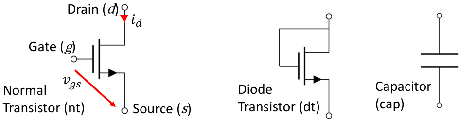
Fig. 3 shows three different device level functional blocks. In addition to capacitors, we define and use two different functional block types for transistors:
3.1 Normal Transistor
Function: A normal transistor establishes a relation between the the voltage potential at the gate of the transistor and the current at the drain of the transistor. Either or is the control factor.
Structure: A normal transistor is a transistor without any self connections.
| (7) |
3.2 Diode Transistor
Function: A diode transistor converts its drain-source current into a stable gate-source voltage .
Structure: A diode transistor is a transistor , whose drain is connected to its gate :
| (8) |
4 Functional Blocks on Hierarchy Level 2
The majority of the functional blocks on HL 2 consist of transistor stacks. Typical transistor stacks are shown in Fig. 4, 5. A transistor stack is a set of 1-3 transistors having the same doping and a drain-source connection i.e., the drain of a lower transistor in the stack is connected with the source of the next higher transistor . Higher transistor gates are not allowed to be connected to drains of lower transistors. Drains of higher transistors are not allowed to be connected to lower transistor sources.
| (9) |
The usual number of transistors in a stack is 1-2. For the pins in a transistor stack, the following naming convention will be used. The source not connected to any drain in the stack is the source of the transistor stack. The drain not connected to any source of the stack is the drain of the transistor stack. If all drains or sources of the stack must be considered, numbering will be used. The definition of the transistor stack is in the following used to describe the functional blocks in detail.
4.1 Voltage Bias

Function: A voltage bias converts its drain current into a stable gate-source voltage applied to a gate of a current bias.
Structure: A voltage bias (Fig. 4) consists of a transistor stack with the gates of its devices connected to gates of a current bias with same doping as . Additionally, the drain of the stack must be connected to a gate of . For every gate in the stack, exactly one gate-drain connection with another transistor of same doping exists. This transistor must be part of a voltage or current bias but not necessarily of or itself.
| (10) |
4.2 Current Bias
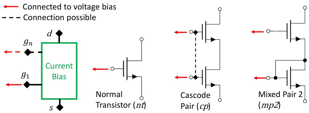
Function: A current bias converts the voltage potential applied at its gates into a drain current .
Structure: A current bias (Fig. 5) consists typically of a stack of normal transistors, which might have a gate connection. In rare cases, the normal transistor at the bottom is exchanged by a diode transistor. The gates of a current bias are connected to a gate or the upper drain of a voltage bias (). The voltage bias must have the same doping. The drain of the upper transistor of a current bias must not be connected to any gate of a voltage bias with same doping.
| (11) |
4.3 Current Mirror

Function: A current mirror provides a current by the current bias, specified by the devices sizes and the current of the voltage bias.
Structure: Fig. 6 shows the structural definition of a current mirror and examples. To form a current mirror , voltage bias and current bias must have equal doping and a source connection. The gates of the voltage bias must be connected to the gates of the current bias. The uppermost drain of the voltage bias must be connected to a gate of the current bias . All gates of the voltage bias with exception of the upper most one must have a connection to a drain of either voltage or current bias
| (12) |
4.4 Differential Pair
Function: A differential pair converts the voltage potentials at the gates of its two input transistor into amplified drain currents. Equal voltages lead to equal drain currents. Depending on the structure, higher amplification gains can be obtained. Cascode versions with four transistors have a higher amplification gain than a simple version with two transistors.
Structure: Fig. 7 shows the structure of a differential pair. The basic structure is the simple differential pair, which can also stand alone.

A simple differential pair consist of two normal transistors connected only at their sources. This common source must be connected to a current bias drain . The two normal transistors and the current bias must have equal doping.
| (13) |
For the cascode version of the differential pair , a simple differential pair is connected with its drains to the sources of a gate connected couple . These are two normal transistor with same doping connected at their gates:
| (14) |
The structural definition of the cascode version of the differential pair is:
| (15) |
Two types of cascode variants exist having different doping characteristics. In the folded cascode differential pair , and have opposite doping:
| (16) |
In the cascode differential pair , they have equal doping:
| (17) |
4.5 Analog Inverter

Function: An analog inverter inverts and amplifies an input voltage applied at one of its gates.
Structure: An analog inverter (Fig. 8) consists of two normal transistor stacks differing in doping. The stacks are connected at their drains . The two sources are connected to the supply voltage rail that corresponds to the doping type. Gate-gate, gate-drain and source-source connections between transistors are not allowed.
| (18) |
4.6 Multiple Assignments of Transistors to Functional Blocks
Hierarchy level 2 is the only level which allows transistors to be part of more than one functional block. An example are current mirrors. According to (12), every transistor in a current mirror is at the same time part of a voltage or current bias . We distinguish between relevant, irrelevant and false multiple assignments.


Relevant multiple assignments are circuitry-wise correct and obtain additional information needed to find other functional blocks. These are the above mentioned double assignments in current mirrors, different current mirrors with the same voltage bias but different current biases forming a current mirror bench, and the two cases shown in Fig. 9. Fig. 9a shows a gate connected couple (14) in two current biases . The gate connected couple must be part of a cascode version of a differential pair (15). The transistors are therefore part of and or . Fig. 9b shows an analog inverter with a transistor stack that is also part of a current mirror . Thus, is part of and the current bias in .
Irrelevant multiple assignments are circuitry-wise correct but do not obtain any additional information to the functional behavior as the functional blocks the transistor is in are of the same type. An example is a simple current mirror in a cascode current mirror (Fig. 10a). The simple current mirror does not obtain any additional information to the cascode current mirror. To avoid such irrelevant multiple assignments of transistors following rule is used:
| (19) |
contains all functional blocks which are potential irrelevant. These are all current mirrors, voltage and current biases.
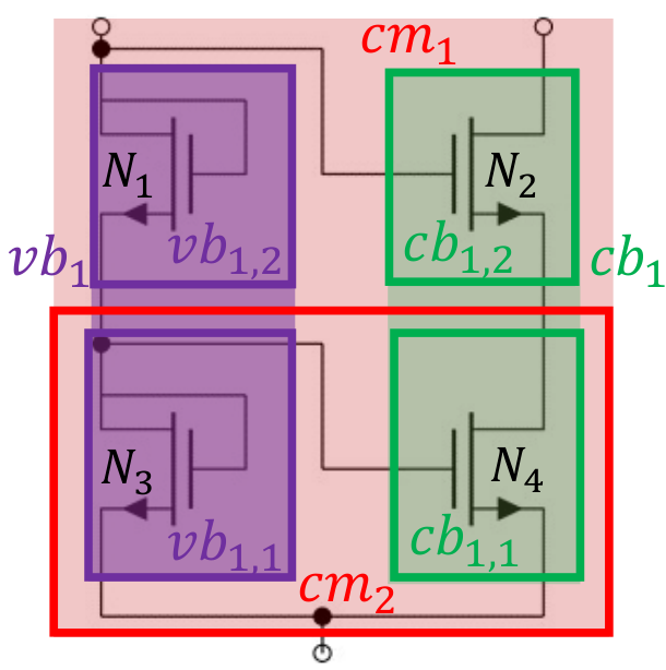
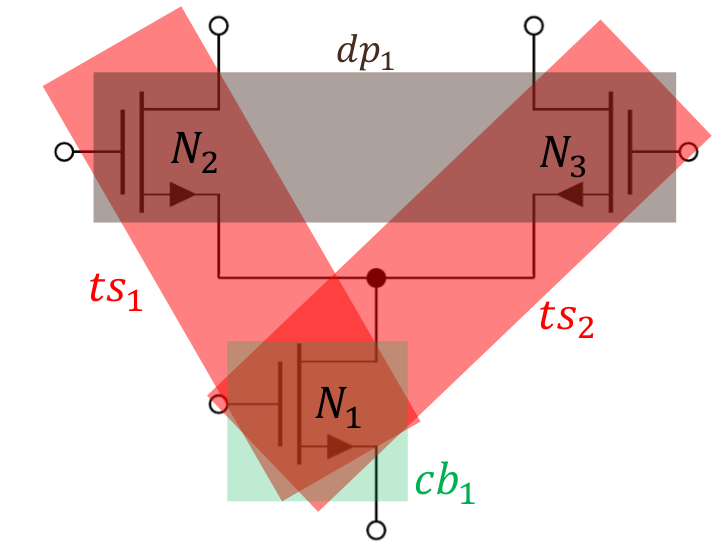
False multiple assignments are circuitry-wise incorrect, e.g., two transistor stacks in a differential pair with current bias (Fig 8). With suitable transistors connected at the drain of the differential pair, these false transistor stacks might form analog inverters. By suppressing the recognition of these transistor stacks, the false recognition of analog inverters is omitted.
5 Functional Blocks on Hierarchy Level 3
On HL 3 are the functional block types that form the amplification stages (HL 4) of an op-amp, i.e., transconductance, load and stage bias.
5.1 Transconductance
Function: A transconductance converts a voltage potential applied at its gates into an (amplified) current.
Structure: Fig. 11 shows the structural definition of a transconductance as well as examples. Two different types of transconductance exist, non-inverting and inverting.

A non-inverting transconductance consists of 1 or 2 differential pairs. We further define three different types having three different structures:
A simple transconductance is a transconductance consisting of one differential pair, having no gate connection to any other differential pair.
| (20) |
A complementary Transconductance consists of two differential pairs with opposite doping and connected at both gates
| (21) |
A common-mode feedback (CMFB) transconductance consists of two differential pairs with equal doping connected at one of the two gates:
| (22) |
A inverting transconductance consists of a transistor stack of normal transistors, with the source connected to a supply voltage rail. No gate-gate and gate-drain connection of the transistors in the stack is allowed. The gate of the bottom transistor in the stack is connected to the output of another transconductance or to the output of a load . The drain of the stack is connected to the output of a stage bias .
| (23) |
The definition of the load is given in the next section. The definition of the stage bias is given in Sec. 5.3.
5.2 Load
Function: A load converts a current into a voltage. It influences the gain generated by the connected transconductance.
Structure: Fig. 12 shows the structure of a load . A load consists of one or two load parts of type . The parts are connected at their drains and have different substrate types. If a gate connected couple is in one of the load parts, its sources are connected to the output of a transconductance of type . Otherwise, if no gate connected-couple is in one of the load parts, the outputs of the load are connected to .
| (24) |
A single load part consists of one or two transistor stacks, which have gate-gate connections. A transistor stack in a load part is either of type voltage or current bias. If no gate connected-couple is in the load part, the sources must be connected. The doping of the transistor stacks is equal.
| (25) |
5.3 Stage Bias
Function: A stage bias supplies a transconductance with defined currents.
Structure: A stage bias is a subtype of the type bias (Fig. 13). Two different types exist.
A bias with voltage output consists of voltage and current biases with . Its input is the drain of a voltage bias. The outputs are gates of voltage biases, which are connected to gates of other functional blocks. All current biases in must have a drain-drain connection to a voltage bias with opposite doping and a gate-gate connection to a voltage bias with equal doping in .
| (26) |
A bias with voltage output is a stage bias, iff it consists of exactly one voltage bias , which is connected with its drain to the output of a transconductance of type inverting:
| (27) |
In all other cases, if a bias with voltage out consists of more than one voltage bias or if it is not connected with its input pin to a transconductance, it is the circuit bias (Sec. 6.2)
A bias with current output consist of current biases. Its inputs are the gates of the current biases. The outputs are the drains of the current biases, which must be connected to the source or output of a transconductance.
| (28) |
A bias with current output is always a stage bias:
| (29) |
6 Functional Blocks on Hierarchy Level 4
The functional block types on HL 4 are the amplification stage, the circuit bias, the compensation and load capacitor.
6.1 Amplification Stage
Function: Two functional types of amplification stage exist: the amplification stage of an op-amp and the common-mode feedback stage . The amplification stage amplifies the input signal for the time. A common-mode feedback (CMFB) stage amplifies the output signals of a fully differential op-amp while comparing them to a reference voltage and feeds them back to the amplifier.
Structure: Fig. 14 shows the general composition of the amplification stages of an op-amp. Every amplification stage has at least two inputs and one output. It has a source connection to both supply voltage rail. Two structural types of amplification stages exist, non-inverting and inverting amplification stages. Non-inverting amplification stages are the first stage of an op-amp and the CMFB stage. Inverting stages form the further stages of an op-amp (). In the following, both types are described in detail.
A non-inverting amplification stage consists of a transconductance , a load and a stage bias . The transconductance must be of type non-inverting and the stage bias must have a current output connected to the sources of the transconductance. The load outputs or the sources of a gate connected couple in the load must be connected to the outputs of the transconductance.
| (30) |
Non-inverting amplification stages are classified into three types: simple first stage , complementary first stage , and CMFB stage . The types differ in the transconductance types and the doping characteristics of its functional blocks.
A simple first stage has a transconductance of type . The transconductance and the stage bias have the same substrate type, while the load has either the opposite doping or mixed doping.
| (31) |
A complementary first stage has a transconductance of type . Transconductance, load and stage bias have all mixed doping.
| (32) |
A common-mode feedback stage has a transconductance of type . Transconductance and stage bias have the same substrate type, while the load has opposite doping.
| (33) |
A inverting amplification stage consists of a transconductance and a stage bias with opposite doping connected at their outputs. The transconductance must be of type inverting. The stage bias consists either of one voltage bias or one current bias.
| (34) |
Note, that all inverting stages can occur twice in an op-amp, e.g., two second stages. It appears when the op-amp is fully differential or a symmetrical op-amp (Fig. 2, with ).
Differentiating between an inverting stage with a stage bias with current output and an inverting stage with a stage bias with voltage output allows to give a more precise definition of inverting amplification stages:
A inverting stage with stage bias with current output must also fulfill the type definition of an analog inverter to be a valid inverting amplification stage:
| (35) |
Note, that not all analog inverters are inverting stages, as the constraints for a transconductance (23) and stage bias (28) must hold.
A inverting stage with stage bias with voltage output only occurs in symmetrical OTAs, which are op-amps with a characteristic first stage and two second stages (Fig. 2). The first stage must be a simple first stage having a load consisting of two voltage biases with same doping. Both voltage biases must have a gate-gate connection to a transconductance in a second stage of type . One second stage must be of type . The other second stage must have a voltage bias as stage bias, which has a gate-gate connection to the stage bias of :
| (36) |
6.2 Circuit Bias
Function: The circuit bias supplies all functional blocks of type amplification stage with voltages specified by .
6.3 Compensation Capacitor
Function: A compensation capacitor increases the stability of an op-amp.
Structure: A compensation capacitor is connected between the outputs of two different amplification stages :
| (38) |
6.4 Load Capacitor
Function: The load capacitor represents the capacitive load the op-amp is able to drive in its application.
Structure: A load capacitor is connected between an output of the highest (-th) amplification stage and ground:
| (39) |
7 Functional Block Analysis
The functional block analysis recognizes all functional blocks in an op-amp netlist based on the definitions given in Sec. 3 - 6. Fig. 15 shows the dependency graph that arises from these definitions. Note, that bidirectional dependencies exist. Therefore complex algorithms are required for the functional block analysis.
7.1 Hierarchy Level 1
On hierarchy level 1, the definitions of the functional block types are independent of each other. Therefore, the definitions given in Sec. 3 can be used for recognition without any restriction to their order.
7.2 Hierarchy Level 2
On level 2, every recognition of a functional block type depends on another functional block on the same level (10) - (18). Voltage bias and current bias are at the starting point of the dependency graph being bidirectionally dependent. Alg. 1 presents the recognition algorithm.
To resolve all dependencies, we propose to start with the recognition of transistor stacks (9), which are auxiliary blocks independent of all functional block types of level 2. On basis of the recognized transistor stacks, the current and voltage biases are recognized. For every substrate type, a set of transistor stacks is created (Line 3, 4). The algorithm iterates over both sets. It searches for two transistor stacks , which are connected at their gates and also have a drain-gate connection (Line 7). This corresponds to the definition of a voltage bias (10), taking as voltage bias connected to a current bias . It is checked if has all the gate-drain and gate-gate connections to needed for a current bias (Line 8), and if it is not connected with its drain to any gate of a transistor stack in . This corresponds to the definition of a current bias (11). If this is the case, the and are primary voltage and current biases, i.e., they have all gate-gate and gate-drain connection to each other. Another case is that is an already identified current bias (Line 11). In this case, the primary voltage and current bias were already recognized and a secondary voltage bias is recognized, e.g. a voltage bias which biases the uppermost gate of a wide-swing cascode current mirror. Note, that the last part of the voltage bias definition (10) is not checked as this is always ensured by using an valid op-amp topology.
The repetitive iteration over all recognized transistor stacks is needed to ensure that all secondary voltage biases are found. After finding all voltage and current biases. The current mirrors and differential pairs are found using their definitions. The analog inverter is the last functional block of HL 2, which is recognized to omit their false recognition in differential pairs. With (19) all irrelevant functional blocks are deleted from the set of all functional blocks.
7.3 Hierarchy Level 3 - 4
We combine the recognition of the functional block types of HL 3 and HL 4 as this simplifies the recognition process and resolves the bidirectional dependency of the inverting transconductance and its stage bias . The algorithm (Alg. 2) starts by recognizing all non-inverting transconductances. They are the only functional blocks on HL 3 that are independent of any other functional block (30).
In the next step, the loads are recognized. Here we propose not to use the exact definition of the load (24) but instead use the algorithm shown in Alg. 3. The advantage of this algorithm is that it does not depend on recognized voltage or current biases as the definition (25) does. Often external voltage biases are used to bias the load. In this case, current biases as load are not recognized. Alg. 3 is more general and uses transistor stacks for recognition. It first searches for the nets, to which the load parts are connected (Line 4 - 9). This is either the drain net of a gate connected couple or if no exists, the drain nets of differential pairs in . At these nets, the algorithm searches for the transistor stacks forming the load (Line 12 - 19). Note, that a gate connected couple if recognized, is part of a load while a differential pair is not.
After the recognition of the loads, the stage biases of non-inverting stages are recognized by definition (29). With the non-inverting transconductances, loads and stage biases, the non-inverting stages are recognized.
In the next step, inverting stages are recognized. For recognition, we use that an inverting stage is also a functional block of type analog inverter iff its stage bias is of type current bias (35). This resolves the bidirectional dependency of an inverting transconductance and its bias . The algorithm iterates over all recognized analog inverters. For every analog inverter, it is checked, if one of its stacks is connected with its first gate to the output of an already recognized stage . This corresponds to the definition of an inverting transconductance (23). The output of a stage is either the output of its load or the output of its transconductance (Fig. 11). The other transistor stack in the analog inverter must be of type current bias and thus is the stage bias (29) of the inverting stage.
After finding the first inverting stage with current bias as stage bias, it is searched for an inverting stage with voltage bias as stage bias (36). This type of inverting stage is only part of an op-amp if the first stage fulfills the criteria of a symmetrical op-amp (Line 17). It is sufficient to search for a transistor stack connected with its gate to one of the voltage biases in the first stage load. must be connected with its drain to a voltage bias drain . The voltage bias must be connected with its gates to the current bias of the already recognized inverting stage .
As inverting stages might be connected to other inverting stages, as, e.g, a third stage, it is repeatedly iterated over the set of analog inverters until no new stage is found. Thus, also multi-stage op-amps are supported by this method. Multi-stage op-amps usually comprise multiple inverting stage. Some of them may be connected in frequency compensation in feedback loops [36, 37]. However, as they have the characteristic structure of an inverter and as the gate of one of the transistors in the transconductance is connected to the output of the previous stage, they are unambiguously identifiable.
After finding all amplification stages of an op-amp, the circuit bias, compensation and load capacitors are recognized using their definitions.
8 Experimental results
In this section, we present experimental results of the functional block analysis. We illustrate the behavior of the algorithms presented in Sec. 7 on the example of a telescopic two-stage op-amp (Fig. 16). Furthermore, we discuss the results of the functional block analysis on three different circuits: a symmetrical op-amp (Fig. 2), a folded-cascode op-amp with CMFB (Fig. 17) and a three-stage op-amp (Fig. 18). Overall more than 4000 different op-amp topologies have been successfully analyzed.
The computational cost of the algorithm is very low. The runtime for every topology is in the area of milliseconds. The time needed to add a new functional block to the algorithm depends on the uniqueness of its structures. It is very low and in the area of a few hours, if many of the already implemented functional blocks are reused. More advanced functional blocks need a day integration time. Frequency compensation methods as described in [38, 39] can be integrated in this method in less than a work day.


Telescopic op-amp (HL 2): Fig. 16a shows all functional blocks recognized on level 2 with Alg. 1. Alg. 1 first searches for all transistor stacks in the circuit sorted according to their substrate type. All transistor stacks are marked in dark blue. Transistor stacks including transistors of the differential pair () are not shown as they are not valid (Sec. 4.6). Every transistor in the circuit is a transistor stack by itself. That means for the three transistor stacks consisting of two transistors, every transistor in these stacks is also a transistor stack by itself. The algorithm checks which of the transistor stacks are voltage and current biases. Note that, for , the transistor stacks of the individual transistors are classified as a current bias and voltage bias, respectively. has a gate connection to the voltage bias and therefore fulfills the definition of a current bias. has a gate-drain connection to itself and therefore is a voltage bias connected with its gate to the gates of the current biases and . The other two transistor stacks and , form a current mirror. The transistor stacks of the individual transistors therefore are irrelevant. Note that does not form current mirrors with and as their sources are not connected to the same net. All voltage and current biases in this circuit are primary. All voltage biases have their needed gate-drain connection (10) by themselves, such that no secondary voltage biases are needed to establish a drain-gate connection of a voltage bias gate. Alg. 1 ends with the recognition of the cascode differential pair (17) and the analog inverter (18).
Telescopic op-amp (HL 3 - HL 4): Fig. 16b shows all functional blocks recognized on levels 3 and 4 with Alg. 2. The algorithm first recognizes the differential pair as simple non inverting first stage transconductance . For the load recognition, the drain nets of are used. form the gate connected couple part of the cascode differential pair . Two load parts are found: The gate connected couple forms the load part with p-doping. The load part with n-doping consists of the current mirror . As stage bias, the current bias is found as it is connected with its drain to the source of . With it, all parts of the non-inverting first stage are recognized. In the next step, Alg. 2 checks if the inverter recognized on level 2 is a second stage. This is true, as was recognized as current bias and is connected with its gate to one output of the first stage. Because the first stage does not fulfill the criteria of a symmetrical op-amp, it is not searched for an inverting stage with voltage bias as stage bias. The voltage and current biases not part of the two amplification stages are recognized as circuit bias . The recognition ends by identifying the capacitor in the circuit as compensation capacitor.
Symmetrical op-amp with an additional inverting stage: Fig. 2 shows the results of the functional block analysis for a symmetrical op-amp with an additional inverting stage . During the recognition of the inverting stages, first is recognized as inverting second stage . Afterwards is recognized, fulfills the condition of a first stage of a symmetrical op-amp and with , the needed second stage with current bias as stage bias is given (36). The transistor stack fulfills the definition of a non-inverting transconductance (23). is the stage bias with voltage output. The gate-gate connection to the stage bias of is given. Note, that for a correct identification of the exact definition of an inverting stage must be used (34). As has a gate connection to one output of the first stage, a drain of the differential pair, it is considered as possible inverting transconductance of another second stage. As for this transconductance, no stage bias exist because is not of type bias, it is not recognized as transconductance. Instead, after is recognized, is identified as inverting transconductance, because it has a connection to an output of . is its stage bias.


Folded-cascode op-amp with CMFB: Fig. 17 shows the results of the functional block analysis in a folded-cascode op-amp with CMFB. The four load transistors are externally biased by the pins and respectively. Hence, these four transistors are not recognized as current biases (Fig. 17a) as they are not connected with their gates to a voltage bias. However with Alg. 3, they are still recognized as part of the load (Fig. 17b). is also neither identified as current nor voltage bias as it does not have any gate-gate connections to a another transistor with same doping. However, it fulfills the functional definition of a load as it has a drain-drain connection to . Therefore, it is recognized with Alg. 3 correctly even if it does not fulfill the definition of a load entirely (24).


Three-stage op-amp: Fig. 18 shows the results of the analysis for a three-stage op-amp. Two analog inverters are recognized on HL 2 (Fig. 18a). One of the transistors (), () is identified to be part of a current mirror. The other transistor (), () is not part of any additional functional block on HL 2. After recognizing the first and second stage with Alg. 2, the third stage is recognized (Fig. 18b). With the gate of connected to the drain of , the input of third stage is connected to the output of the second stage (34). is a identified current bias. Hence, fulfills all criteria of a third stage. Alg. 2 ends by identifying the compensation capacitors . Both capacitors a connected between the output of two stages, between the output of first and third stage, between second and third stage. Hence, both capacitors fulfill (38).
9 Application of the Hierarchical Functional Block Decomposition Method
Two applications of the functional block decomposition method are presented: A sizing method (Sec. 9.1, details in [2]) and a structural synthesis method (Sec. 9.2, details in [3]).
9.1 Application to Circuit Sizing
The common manual design process is based on analytical equations as described in [17, 18, 19, 20, 21]. For each functional block described in Secs. 3 - 6, a behavior model can be derived based on these standard equations resulting in a hierarchical performance equation library (HPEL) [2]. For the functional blocks on HL 3, the equations part of the library describe, e.g., the input and output conductance (, ) of a functional block . Following equation for instance holds for the output conductance of a functional block consisting of one or two transistor stacks :
| (40) |
are the output und input conductance of a transistor in with giving the position of the transistor in the transistor stack. There are exceptions to this equation which are discussed in [2].
An equation for the output resistance of an amplification stage functional block on HL 4 is developed based on (40) and the functional blocks of the stage connected to the output net of the stage. These functional blocks can be stage biases, load parts and transconductances.
| (41) |
This equation is part of the equation describing the open-loop gain of a stage which is on the same hierarchy level in the HPEL:
| (42) |
with the input conductance of the stage. The open-loop gain equation of the overall op-amp is part of HL 5 of the HPEL. is the number of all stages in the op-amp,
| Constraints | Spec. | M | S |
|---|---|---|---|
| Gate-area (103 m2) | 15 | 5.8 | - |
| Quiescent power (mW) | 10 | 5.8 | 6.1 |
| Max. common-mode input voltage (V) | 3 | 3.3 | 4.4 |
| Min. common-mode input voltage (V) | 2 | 0 | 0.1 |
| Max. output voltage (V) | 4 | 4.5 | 4.5 |
| Min. output voltage (V) | 1 | 0.3 | 0.2 |
| CMRR (dB) | 90 | 130 | 146 |
| Unity-gain bandwidth (MHz) | 7 | 10 | 7 |
| Open-loop gain (dB) | 80 | 120 | 93 |
| Slew rate () | 15 | 28 | 22 |
| Phase Margin (∘) | 60 | 60 | 67 |
| Variable | Value (m/pF) |
|---|---|
| 172;9 | |
| 27;4 | |
| 247;3 | |
| 515;3 | |
| 7;3 | |
| 7;4 | |
| 43;3 | |
| 90;1 | |
| 90;1 | |
| 130;1 | |
| 269;1 | |
| 166;9 | |
| 6.4 |
Analogously, performance equations for all functional blocks that have been presented in Sec. 3 - Sec. 6 have been established [2]. After a functional block analysis of a given op-amp topology according to the methods presented in the paper, the corresponding performance equations of the functional blocks are automatically composed forming a behavioral model of the op-amp performance. This model forms a Mixed-Integer Non-linear Programming problem (MINLP) for sizing the circuit, which is solved, e.g., with a constraint programming approach [40].
Table 1 shows the results of the sizing method for the telescopic op-amp (Fig. 16) using the specifications given in column 2 of Table Ia. The values calculated with the analytical equations within the sizing method are compared to simulation results using a BSIM3v3 models. The deviations due to the simpler transistor model are less then 30% and within designer expectations.
9.2 Application to Structural Synthesis
The functional block library (Sec. 3 - Sec. 6) can be applied to structural synthesis by functional block composition. Alg. 4 gives an algorithm to create the structural implementations of a functional block based on the implementation of its subblocks and a set of characteristic connections . The two-transistor implementations of a current bias (Fig. 5), e.g., are created based on two structural implementation sets containing normal and diode transistors of the same doping ( ). Every combination of has a drain-source connection (). Thus, all structural implementations of a two-transistor current bias are created. More complex functional blocks need additional rules set as explained in [3].
With Alg. 4, the structural implementations of all functional blocks in Secs. 3 - 6 are created allowing a creation of up to 3000 topologies. The corresponding composition graph is presented in [3]. For given specifications, the topologies are sized and evaluated using an enhanced version of the sizing method described in Sec. 9.1. The respective algorithm is presented in [3]. Table 2 shows the output of the synthesis tool for the specifications in Table Ia. As the specifications are not highly demanding and no upper bounds are specified, many topologies are able to fulfill the specifications, e.g. the telescopic op-amp in Fig. 16. Defining more strict specifications reduces the number of created topologies significantly.
| First stage type | simple | folded-cascode | telescopic | symmetrical | total | |||
| # stages | 1 | 2 | 1 | 2 | 1 | 2 | - | |
| # topologies | 0 | 111 | 0 | 181 | 20 | 77 | 58 | 447 |
10 Conclusion and Outlook
This paper presented a new method to represent op-amps by their functional block. The functional blocks are ordered hierarchically. For each functional block, a systematic functional and structural description is given allowing an automatic recognition. Two different areas of applications are presented: Together with a performance equation library, the functional block analysis allows a topology-independent sizing of op-amps. A functional block composition method allows structural synthesis of op-amps. Thousands of different op-amp topologies are created based on hierarchically generated functional blocks by small rule sets.
Future work remains in including more feedback compensation techniques in the method. Currently, a compensation capacitor is supported in the recognition algorithm. For multi-stage op-amps, additional compensation circuits as, e.g., [38, 39] are needed. As they have a fixed structure, the compensation circuits can be added to the method. Future research will also be on including the functional block composition method in layout synthesis.
References
- [1] G. Shi, Automatic stage-form circuit reduction for multistage opamp design equation generation, ACM Transactions on Design Automation of Electronic Systems (Oct. 2019). doi:10.1145/3363499.
- [2] I. Abel, M. Neuner, H. Graeb.
- [3]
I. Abel, H. Graeb, Structure Synthesis
of Basic Op-Amps by Functional Block Composition, .
URL http://arxiv.org/abs/2101.07517 - [4] M. d. Hershenson, S. P. Boyd, T. H. Lee, Optimal design of a CMOS op-amp via geometric programming, IEEE Transactions on Computer-Aided Design of Integrated Circuits and Systems (2001).
- [5] P. C. Maulik, L. R. Carley, R. A. Rutenbar, Integer programming based topology selection of cell-level analog circuits, IEEE Transactions on Computer-Aided Design of Integrated Circuits and Systems (1995).
- [6] A. Gerlach, J. Scheible, T. Rosahl, F. Eitrich, A generic topology selection method for analog circuits with embedded circuit sizing demonstrated on the OTA example, in: Design, Automation Test in Europe Conference Exhibition, 2017.
- [7] A. Graupner, R. Jancke, R. Wittmann, Generator based approach for analog circuit and layout design and optimization, in: Design, Automation Test in Europe, 2011.
- [8] A. Das, R. Vemuri, A graph grammar based approach to automated multi-objective analog circuit design, in: Design, Automation Test in Europe Conference Exhibition, 2009.
- [9] T. McConaghy, P. Palmers, M. Steyaert, G. G. E. Gielen, Trustworthy genetic programming-based synthesis of analog circuit topologies using hierarchical domain-specific building blocks, IEEE Transactions on Evolutionary Computation (2011).
- [10] H. Graeb, S. Zizala, J. Eckmueller, K. Antreich, The sizing rules method for analog integrated circuit design, in: IEEE/ACM International Conference on Computer Aided Design, 2001.
- [11] T. Massier, H. Graeb, U. Schlichtmann, The Sizing Rules Method for CMOS and Bipolar Analog Integrated Circuit Synthesis, IEEE Transactions on Computer-Aided Design of Integrated Circuits and Systems (2008).
- [12] M. Meissner, L. Hedrich, FEATS: Framework for Explorative Analog Topology Synthesis, IEEE Transactions on Computer-Aided Design of Integrated Circuits and Systems (2015).
- [13] Z. Zhao, L. Zhang, An Automated Topology Synthesis Framework for Analog Integrated Circuits, IEEE Transactions on Computer-Aided Design of Integrated Circuits and Systems (2020).
- [14] M. Eick, H. Graeb, MARS: Matching-Driven Analog Sizing, IEEE Transactions on Computer-Aided Design of Integrated Circuits and Systems (2012).
- [15] H. Li, F. Jiao, A. Doboli, Analog circuit topological feature extraction with unsupervised learning of new sub-structures, in: Design, Automation Test in Europe Conference Exhibition, 2016.
- [16] M. Neuner, I. Abel, H. Graeb, Library-free structure recognition for analog circuits, in: Design, Automation Test in Europe Conference Exhibition, 2021.
- [17] D. R. H. Phillip E. Allan, CMOS Analog Circuit Design, Oxford University Press, 2012.
- [18] K. R. Laker, W. M. C. Sansen, Design of analog integrated circuits and systems, McGraw-Hill, 1994.
- [19] W. M. C. Sansen, Analog Design Essentials, Springer, 2007.
- [20] D. Johns, K. Martin, Analog Integrated Circuit Design, John Wiley and Sons, 1997.
- [21] P. R. Gray, R. G. Meyer, P. J. Hurst, S. H. Lewis, Analysis and Design of Analog Integrated Circuits, 4th Edition, John Wiley & Sons, Inc., USA, 2001.
- [22] M. G. R. Degrauwe, O. Nys, E. Dijkstra, J. Rijmenants, S. Bitz, B. L. A. G. Goffart, E. A. Vittoz, S. Cserveny, C. Meixenberger, G. van der Stappen, H. J. Oguey, IDAC: An interactive design tool for analog CMOS circuits, IEEE Journal of Solid-State Circuits (1987).
- [23] F. El-Turky, E. Perry, BLADES: An artificial intelligence approach to analog circuit design, IEEE Transactions on Computer-Aided Design of Integrated Circuits and Systems (1989).
- [24] R. Harjani, R. A. Rutenbar, L. Carley, OASYS: A Framework for Analog Circuit Synthesis, IEEE Transactions on Computer-Aided Design of Integrated Circuits and Systems (1989).
- [25] H. Y. Koh, C. H. Sequin, P. R. Gray, OPASYN: a compiler for CMOS operational amplifiers, IEEE Transactions on Computer-Aided Design of Integrated Circuits and Systems (1990).
- [26] G. Van der Plas, G. Debyser, F. Leyn, K. Lampaert, J. Vandenbussche, G. Gielen, W. Sansen, P. Veselinovic, D. Leenaerts, AMGIE–A Synthesis Environment for CMOS Analog Integrated Circuits, IEEE Transactions on Computer-Aided Design of Integrated Circuits and Systems (2001).
- [27] K. Antreich, H. Graeb, C. Wieser, Circuit analysis and optimization driven by worst-case distances, IEEE Transactions on Computer-Aided Design of Integrated Circuits and Systems (1994).
- [28] E. S. Ochotta, R. A. Rutenbar, L. R. Carley, Synthesis of High-Performance Analog Circuits in ASTRX/OBLX, IEEE Transactions on Computer-Aided Design of Integrated Circuits and Systems (1996).
- [29] B. Liu, F. V. Fernandez, G. Gielen, Efficient and Accurate Statistical Analog Yield Optimization and Variation-Aware Circuit Sizing Based on Computational Intelligence Techniques, IEEE Transactions on Computer-Aided Design of Integrated Circuits and Systems (2011).
- [30] G. Berkol, E. Afacan, G. Dundar, A. E. Pusane, F. Baskaya, A novel yield aware multi-objective analog circuit optimization tool, in: IEEE International Symposium on Circuits and Systems, 2015.
- [31] F. Passos, E. Roca, J. Sieiro, R. Fiorelli, R. Castro-Lopez, J. M. Lopez-Villegas, F. V. Fernandez, A Multilevel Bottom-up Optimization Methodology for the Automated Synthesis of RF Systems, IEEE Transactions on Computer-Aided Design of Integrated Circuits and Systems (2019).
- [32] A. Canelas, R. Povoa, R. Martins, N. Lourenco, J. Guilherme, J. P. Carvalho, N. Horta, FUZYE: A Fuzzy C-Means Analog IC Yield Optimization using Evolutionary-based Algorithms, IEEE Transactions on Computer-Aided Design of Integrated Circuits and Systems (2019).
- [33] T. McConaghy, P. Palmers, M. Steyaert, G. G. E. Gielen, Variation-Aware Structural Synthesis of Analog Circuits via Hierarchical Building Blocks and Structural Homotopy, IEEE Transactions on Computer-Aided Design of Integrated Circuits and Systems 28 (9) (2009).
- [34] F. H. Bennett, M. A. Keane, D. Andre, J. R. Koza, Automatic Synthesis of the Topology and Sizing for Analog Electrical Circuits using Genetic Programming , in: EUROGEN workshop in Jyvdskyld, Finland, 1999.
- [35] C. Ferent, A. Doboli, Novel circuit topology synthesis method using circuit feature mining and symbolic comparison, in: Design, Automation Test in Europe Conference Exhibition, 2014.
- [36] Ka Nang Leung, P. K. T. Mok, Analysis of multistage amplifier-frequency compensation, IEEE Transactions on Circuits and Systems I: Fundamental Theory and Applications 48 (9) (2001).
- [37] J. Ramos, Xiaohong Peng, M. Steyaert, W. Sansen, Three stage amplifier frequency compensation, in: ESSCIRC 2004 - 29th European Solid-State Circuits Conference, 2003.
- [38] G. Palmisano, G. Palumbo, An optimized compensation strategy for two-stage cmos op amps, IEEE Transactions on Circuits and Systems I: Fundamental Theory and Applications 42 (3) (1995).
- [39] G. Palmisano, G. Palumbo, A compensation strategy for two-stage cmos opamps based on current buffer, IEEE Transactions on Circuits and Systems I: Fundamental Theory and Applications 44 (3) (1997).
- [40] I. Abel, M. Neuner, H. Graeb, COPRICSI: COnstraint-PRogrammed Initial Circuit SIzing, Integration (2020).