Fermi surface chirality induced in a TaSe2 monosheet formed by a Ta/Bi2Se3 interface reaction
Abstract
Spin-momentum locking in topological insulators and materials with Rashba-type interactions is an extremely attractive feature for novel spintronic devices and is therefore under intense investigation. Significant efforts are underway to identify new material systems with spin-momentum locking, but also to create heterostructures with new spintronic functionalities. In the present study we address both subjects and investigate a van der Waals-type heterostructure consisting of the topological insulator Bi2Se3 and a single Se-Ta-Se triple-layer (TL) of H-type TaSe2 grown by a novel method which exploits an interface reaction between the adsorbed metal and selenium. We then show, using surface x-ray diffraction, that the symmetry of the TaSe2-like TL is reduced from D3h to C3v resulting from a vertical atomic shift of the tantalum atom. Spin- and angle-resolved photoemission indicates that, owing to the symmetry lowering, the states at the Fermi surface acquire an in-plane spin component forming a surface contour with a helical Rashba-like spin texture, which is coupled to the Dirac cone of the substrate. Our approach provides a new route to realize novel chiral two-dimensional electron systems via interface engineering that do not exist in the corresponding bulk materials.
keywords
American Chemical Society, LaTeX1 Introduction
Novel functionalities in potential spintronic devices especially involve the locking of the electron’s spin and momentum as realized in Topological Insulators (TIs), as well as in Dirac and Weyl semimetals. The chiral topologic surface state (TSS) in TIs has been found to be very effective in converting a charge current into a spin current which can exert large spin-orbit torques (SOT) in an adjacent ferromagnetic (FM) layer Mellnik et al. 2014; Wang et al. 2015; Fan et al. 2014; Kondou et al. 2016. A critical issue is that the SOT efficiency resulting from the TSS can be influenced by several factors, such as the presence of bulk states, and the band-bending induced appearance of a two-dimensional electron gas, which recently has been shown to be minimized by reducing the Bi2Se3 film thickness Wang et al. 2017. Similarly, transition metal dichalcogenides (TMDCs) with a non-trivial electronic structure containing a heavy metal such as Mo, W, Pt and Pd also have found remarkable interest as spin-source materials from significant charge to spin conversion Yuan et al. 2013; MacNeill et al. 2017; Clark et al. 2018; Xu et al. 2020.
By contrast, the metallic TMDC TaSe2 has a trivial electronic structure in its bulk form and crystallizes in the 2H structure (trigonal-prismatic coordination around tantalum by selenium). In this study we demonstrate that in a van der Waals (vdW) type heterostructure consisting of a single Se-Ta-Se triple-layer (TL) on the (0001) surface of the TI Bi2Se3 a chirality is created in the Fermi surface electronic states. The TaSe2 monosheet is prepared using a novel and simple method. This method, which does not rely on exfoliation or molecular beam epitaxy methods, that have been used in many previous studies, but rather uses an interface reaction between tantalum atoms directly deposited onto a Bi2Se3(0001) substrate. We find that this simple method leads to flat islands that are formed from monosheets of well-ordered TaSe2 with an H-type structure. The absence of the inversion center in the monosheet, in combination with the strong spin-orbit coupling (SOC) that is inherent to TaSe2, results in a spin-splitting of the electronic states at the Fermi energy with oppositely spin-polarized states at the non-symmetry related K and K’ points in the Brilluouin zone (BZ). The SOC lifts the spin-degeneracy of the bands inducing a spin-polarization which pins the electron spins to the out of plane direction. This scenario is referred to as an "Ising-SOC". Until now, it has been generally assumed that monosheets of TMDC’s are bulk-like. Surface xray diffraction (SXRD) analysis provides clear evidence for the vertical relaxation of the central tantalum atom in the prismatic selenium environment thereby lifting the horizontal mirror plane and lowering the point group symmetry from D3h to the C3v. We then used spin- and momentum resolved photoemission spectroscopy, in combination with ab-initio calculations, to study the effect of the structural relaxation on the electronic structure. We find a very important consequence is that the spin-polarized states at the Fermi surface (FS) acquire an in-plane spin component, in this way creating a chirality. Such a low-symmetry monosheet may serve as an efficient spin-source material not only avoiding difficulties encountered by bulk and free electron states in Bi2Se3 but also enabling a more sophisticated out of plane SOT to manipulate perpendicularly magnetized ferromagnetic films, as recently demonstrated in a WTe2/permalloy heterostructure MacNeill et al. 2017
2 Results and discussion
2.1 Structure Analysis
The TaSe2 monosheet was prepared by depositing a sub-monolayer amount of tantalum on a pristine surface of a Bi2Se3(0001) single crystal, followed by annealing at 480∘C for several minutes. Fig. 1 (a) and (b) show low energy electron diffraction (LEED) patterns of the pristine and TaSe2 covered Bi2Se3(0001). The pristine Bi2Se3(0001) surface exhibits a threefold symmetric LEED pattern indicating the absence of crystal twinning. After preparation of the TaSe2 monosheet, the substrate spots are attenuated and new spots appear that are related to the formation of a TaSe2 monosheet [see Fig. 1 (b)]. The in-plane lattice parameter is derived from the spot position at approximately 1.19 reciprocal lattice units (r.l.u.) relative to the first order Bi2Se3 substrate spots. We find a0=b0=348 pm, which corresponds to a tensile strain of 1.5% as compared to that of bulk 2H-TaSe2 (343 pm) Brown and Beerntsen 1965.
The tantalum covered surface was studied by scanning tunneling microscopy (STM) as outlined in Figure 2 (a) and (b). The Bi2Se3(0001) surface is characterized by terraces several hundred nanometers wide, which are separated by steps, 950 pm in height, that corresponds well with the thickness of a single quintuple layer (QL) of Bi2Se3. The structure of Bi2Se3 is composed of QLs, each consisting of Se-Bi-Se-Bi-Se layers, that are separated by a van-der-Waals (vdW) gap. The QLs themselves are stacked in an A-B-C-A… sequence. In the constant current STM image in Fig 2(a) (U V, I pA) TaSe2 islands on the terraces appear as bright elevations with an apparent height of approximately 600 pm. The profile along the white line is given in Figure 2(b). It reflects the 950 pm high QL steps and the 600 pm high islands. Based on the STM images, the islands can be attributed to a monosheet of TaSe2, whose height is expected to be approximately equal to 600 pm, i.e. half the unit cell lattice parameter c0=1.271 nm of bulk 2H-TaSe2 Brown and Beerntsen 1965. Based on these observations it can be concluded that the interface between the TaSe2 triple layer and the first Bi2Se3 QL is characterized by the Se-Ta-Se/Se-Bi-Se-Bi-Se layer sequence, i.e. the interface is vdW-like. This conclusion is supported by the lattice parameters of the film being close to that of bulk TaSe2 with an incommensurate film to substrate relationship and by the observation that sample annealing beyond 480∘C leads to the evaporation of the film. Based on the STM image alone, no unambiguous assignment of the film structure to H- or T-type can be made, since the height of the polyhedron is nearly identical in both polytypes Yan et al. 2015.
Detailed structural characterization was carried out by SXRD at the beamline BM25b of the European Synchrotron Radiation Facility (ESRF) in Grenoble (France) using a six-circle UHV diffractometer. In Fig. 3 the experimental intensities, I(hk)2, along several rods in reciprocal space are plotted on a log-scale versus momentum transfer (qz) normal to the sample surface. In total, 86 symmetry independent reflection intensities were collected. In contrast to bulk crystals, the coordinate =qz/c⋆ in reciprocal lattice is a continuous (non-integer) parameter owing to the missing lattice periodicity along the c-axis of the monosheet. The reciprocal lattice unit refers to the the Bi2Se3 substrate where c⋆=1/c0=1/(2.864 nm)=0.349 nm-1. A continuously varying intensity distribution is observed, reflecting the presence of an ultra-thin structure along the surface normal. The wide "bell-shaped" intensity profile, which is observed along all rods can be viewed as a finite size broadened Bragg-reflection from the monosheet.
Quantitative analysis was carried out by fitting the experimental intensities to the observed ones. Owing to the high symmetry of the crystal structure, that belongs to the plane group , the structure analysis is straightforward. All atoms are located at high symmetry positions as follows: Se at (0,0,0) [Wyckoff position (1a)], Ta at (1/3,2/3, z) [Wyckoff position (1b)] M.I. Aroyo 2016 and the top-layer Se atom at (0,0,z). The only free positional parameters are the z-positions of the tantalum and the second selenium atom at the top of the Se-Ta-Se triple layer. In addition, an overall scale factor and a Debye-parameter (B=8<u>2), reflecting thermal and static disorder Kuhs 1992, were allowed to vary.
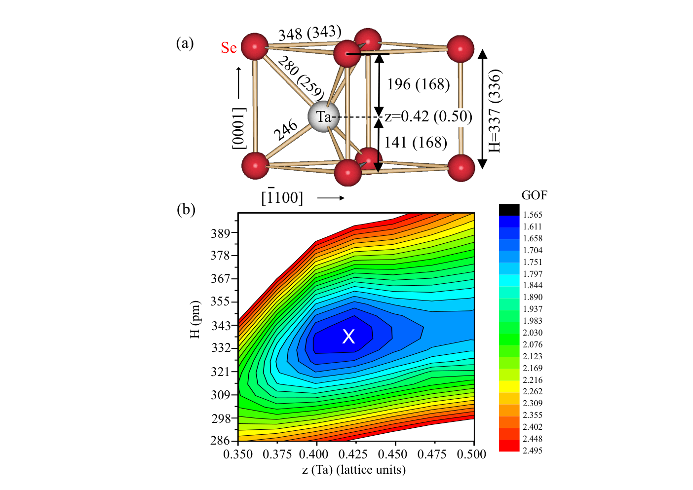
Solid lines in Fig. 3 represent the calculated intensities based on the structure model sketched in Fig: 4(a). The fit quality is measured by the Goodness of Fit (GOF) parameter and the un-weighted residuum (Ru) RuI. We derive values of GOF=1.56 and Ru=0.16. These values can be seen as very satisfactory. We note that the simulation also takes into account the presence of two rotational domains of the TaSe2 unit cell with respect to the trigonal substrate surface. This is done by calculating the incoherent average of the structure factor magnitudes related to each of the two mutually 60∘ oriented domains. The twinning of the film structure is also the reason why the corresponding LEED spots exhibit a sixfold rather than a threefold symmetry. Fig. 4(a) shows a schematic diagram of the structure derived from the optimal fit.
Small (red) and large (grey) balls represent selenium and tantalum atoms, respectively. The H-type monosheet is only one TL thick and stacked as in the bulk. Numbers indicate distances in picometers (pm) with those in brackets referring to bulk values in 2H-TaSe2 Brown and Beerntsen 1965. The most important result is that the central tantalum atom is not located in the center of the prism at z=0.5 in relative lattice units (l.u.) but is rather shifted vertically to z=0.42 l.u. Simultaneously, the height of the TL is slightly increased from 336 pm in the bulk to 337 pm in the monosheet [see numbers in brackets in Fig. 4(a)]. The downward shift of the tantalum atom by about 27 pm out of the center position involves modifications of the interatomic distances also. The nearest Ta-Se distance, which in bulk 2H-TaSe2 is equal to 259 pm, is modified to 280 and 246 pm corresponding to the upper and lower selenium atoms, respectively. We have carefully evaluated the uncertainty of the distance determination as shown in Fig. 4(b) where the GOF is plotted versus the height (H) of the TL and the relative position (z) of the tantalum atom. The cross marks the global minimum at H=337 pm and z=0.42. Each contour level represents a step of 3% with respect to the previous level. The uncertainty of H and z can be estimated by the variation of the GOF upon variation of H and z. An increase of the GOF by 3% over the minimum is viewed as significant, especially here since the basic structure is unaffected by the very small modifications of H and z and because of the large number of independent reflections (86) relative to the number of free parameters (only two positional and one ADP).
Under this assumption we find uncertainties of 5 pm and z=0.02 lattice units, the latter corresponding to 7 pm. As a consequence of the atomic shift, the symmetry of the H-type prism is lowered from D3h (2m) to C3v (3m), which allows for the appearance of an in-plane component of the spin-polarization, as will be shown by spin- and momentum resolved photoemission experiments and by ab-initio calculations in the following.
2.2 Electronic Structure
Spin- and momentum resolved photoemission experiments using a spin-resolving momentum microscope Tusche et al. 2015 were carried out at the NanoESCA beamline Schneider et al. 2012 of the Elettra Synchrotron in Trieste (Italy). The sample was kept at 80 K and p-polarized light and a photon energy of =40 eV were used. The incident photon beam lies in the plane at an angle of 25∘ above the surface plane. By utilizing spin-resolving momentum microscopy, a wide acceptance angle of photoelectrons up to 90∘ can be simultaneously collected. The measured momentum discs provide a comprehensive access to the spin-resolved electronic states in two-dimensional (, ) reciprocal-space momentum maps of the photoemission intensity throughout the entire surface Brillouin zone (SBZ). Furthermore, by scanning the binding energy , the complete information of three-dimensional (, ) maps, containing band dispersion along all directions of the SBZ, can be obtained Suga and Tusche 2015.
Figure 5 (a) and (b) show the spin-averaged band structure of the pristine and the TaSe2 covered Bi2Se3(0001) surface along directions between the high-symmetry points of the first SBZ. The energy range lies between EF and 2.0 eV binding energy (EB). The pristine surface exhibits a well-resolved Topological Surface State (TSS), namely a "Dirac cone" with the Dirac point (DP) located about 350 meV below EF, that is related to n-doping due to selenium defects. The TSS is stable upon formation of the TaSe2 monosheet [Figure 5(b)], but the DP is shifted downwards in energy by approximately 150 meV, indicating further n-doping, possibly by a higher concentration of selenium defects or by charge transfer from the film to the substrate. The observed band structure of TaSe2 monosheet is similar to that of bulk 2H-TaSe2, verifying that the Se-Ta-Se TL is indeed of the H-type. However, there are some differences, for instance, the number of bands crossing EF as discussed in several previous studies Yan et al. 2015; Ryu et al. 2018; Ge and Liu 2012. The TaSe2 monosheet is metallic, there is a Ta-5d related band which crosses EF between and . Deeper lying and also strongly dispersive bands in the binding energy range between 1 and 2 eV are related to Se-p states Ge and Liu 2012. The spin-resolved band structure of the TaSe2 covered sample shown in Figure 5(c) reveals that there is an antiparallel alignment between the spin texture of the TSS and that of the Ta-5d derived states which cross EF between the and the point.
Figures 6(a-c) compare the experimental spin-integrated momentum map at the Fermi Level (EF) with the calculated FS within the first surface Brillouin Zone (SBZ). The FS of the TaSe2 monosheet is characterized by circular hole pockets around the - and the -point as well as the "dog-bone" like electron pocket around the -point, the latter being a consequence of spin-orbit coupling (SOC) and the lack of inversion symmetry in the TaSe2 monosheet Yan et al. 2015; Ge and Liu 2012. Calculated momentum maps are superimposed on the experimental ones for z=0.38, z=0.43 and z=0.50. Direct inspection clearly reveals that the details of the FS sensitively depend on the z-position of the tantalum atom. While for z=0.38, the -pocket is too close to the point, it moves outward until the vertical tantalum position reaches z=0.43. At this point the experimental and the calculated FS fit fairly well, both with regard to size and location of the pockets. Increasing z beyond 0.43 only leads to an increase of the size of the hole pocket, rather than to a further outward shift. This is demonstrated in more detail in Figures 6(d-h) showing the shift and the increase in size with increasing z. The optimum match between calculation and experiment is found for z=0.43, which is in perfect agreement with the SXRD analysis.
In non-magnetic solids the generation of spin-polarized electronic states requires the breaking of the global symmetry. The transition from bulk 2H-TaSe2 with its inversion symmetric P63/mmc space group (D6h point group) to the "unrelaxed" 1H-TaSe2 monosheet with plane group symmetry (absence of inversion symmetry) represents such a case. The SOC lifts the spin-degeneracy of the bands inducing a spin-polarization which pins the electron spins to the out of plane direction. This scenario is referred to as "Ising-SOC" and is regarded as being responsible for the strong enhancement of the critical field HC2 in superconducting TMDC’s such as in monosheet thick H-NbSe2 Bawden et al. 2016; Zhou et al. 2016; He et al. 2018; Sohn et al. 2018 and gated MoS2 Lu et al. 2015; Saito et al. 2015. Most importantly, in the H-TaSe2 monosheet studied here, the point group symmetry is further lowered from D3h, to C3v by the vertical shift of the tantalum atom.
In consequence of the reduced symmetry of the TaSe2 monosheet a pronounced in-plane spin-polarization is observed. The spin-resolved momentum map at the FS is displayed in Fig. 7(a). It shows the in-plane projected spin-polarization which is coded as parallel (red) and antiparallel (blue) to the y direction, being the same as the direction of the incident beam. The spin-resolved momentum-map shows that the TaSe2 monosheet related states at EF exhibit a pronounced in-plane spin polarization, which is a direct consequence of its low-symmetry structure. In order to investigate this scenario in more detail we have calculated the spin-resolved states at EF using the fully relativistic Dirac-Kohn-Sham formalism as implemented in the FPLO18 package Koepernik and Eschrig 1999; Eschrig et al. 2004. We carried out these calculations for different z-positions of the tantalum atom within the prism. Figure 5(b) and (c) shows the results for z=0.43 and 0.50, respectively. While the latter refers to the "ideal" D3h symmetric prismatic polyhedron, the first one corresponds to the SXRD derived structure model. The spin-polarization of the states are displayed as projected along the y-axis allowing a direct comparison with experiment. In agreement with the the previous discussion there is no in-plane component of the spin texture for z=0.50. The situation changes if the tantalum atom is allowed to relax to 0.43 (Figure 5(b)]. An in-plane component of the spin texture appears giving rise to a chirality which is opposite to that of the Dirac cone. Comparison between experiment and calculations shows a remarkable correspondence. For instance, in the experimental FS there is a chirality in the circular hole pocket around the -point as well as in the "dog-bone" like electron pocket around the -points. Also the circular state around the K-points is observable, albeit with a weak spectral weight.
Exploiting a simple interface reaction between tantalum adsorbed on the (0001) surface of Bi2Se3 we have prepared a heterostructure interfacing the TSS of Bi2Se3 with a two-dimensional H-type TaSe2-monosheet. The combination of the Dirac-type states of the Bi2Se3 substrate with the SOC split electronic states at EF of the symmetry reduced H-TaSe2 monosheet in its proximity causes a spin-momentum locking in the latter. Our approach provides a new route to realize novel chiral two-dimensional electron systems that do not exist in the corresponding bulk materials and may open new approaches in the field of spin to charge conversion and spin-orbit torques Soumyanarayanan et al. 2016. A non-magnetic TMDC in the ultra-thin film limit appears as advantageous in achieving a large SOT as it avoids the difficulties encountered with Bi2Se3 caused by the appearance of bulk and free electron states directly in contact with the ferromagnetic layer. Also, interesting transport phenomena may arise from the opposite chirality of the states at the - point of the adjacent films. This certainly needs to be explored in future studies. Notwithstanding these exciting possibilities for future research on this particular system, it is important to point out that the method described here can be used to prepare various selenium-based TMDC-layers on Bi2Se3. Our approach can therefore be used to prepare and explore various new and exciting materials and heterostructures.
3 Methods
3.1 Sample preparation
The experiments were carried out in-situ under ultra-high-vacuum (UHV) conditions in different UHV chambers. The (0001) surface of the Bi2Se3 single crystals were cleaned by repeated cycles of mild Ar+ ion sputtering followed by annealing up to 500∘C for several minutes until Auger electron spectroscopy (AES) did not show any traces of carbon and oxygen Roy et al. 2014; Cavallin et al. 2016 and a clear low energy electron diffraction (LEED) pattern was observed. Tantalum was deposited by evaporation from a tantalum rod heated by electron beam bombardment. The amount of tantalum deposited was calibrated by AES, scanning tunneling microscopy (STM) and ex-posteriori by SXRD. TaSe2 is formed by annealing the as prepared sample at 480∘C for several minutes until the LEED diffraction pattern shows extra spots related to the formation of the TaSe2 phase.
3.2 Surface X-Ray Diffraction
The XRD experiments were carried out at the beamline BM25B of the European Synchrotron Radiation Facility (ESRF) using a six circle diffractometer operated in the z-axis mode. The angle of the primary beam (=0.71 Å) was set to =2.0 degrees. Integrated reflections intensities [INTobs(hkl)] were collected by performing omega scans about the sample normal and collecting the reflected beam by using an two-dimensional pixel detector. The INTobs(hkl) were then multiplied by instrumental correction factors Ccorr as outlined in detail in Refs. Schamper et al. 1993; Vlieg 1997 yielding the experimental intensities [Iobs (hkl)] via: Iobs(hkl)=INTobs(hkl) Ccorr. The total uncertainty (1) of the Iobs(hkl) is estimated to about 10% as derived from the reproducibility of symmetry equivalent reflections.
3.3 Spin-and momentum resolved photoemission spectroscopy
Spin- and momentum resolved photoemission experiments using a Spin-resolving momentum microscope Tusche et al. 2015 were carried out at the NanoESCA beamline Schneider et al. 2012 of the Elettra Synchrotron in Trieste (Italy). The sample was kept at 80 K, and photoelectrons from the TaSe2 valence band region were excited by using p-polarized light and a photon energy of =40 eV. Photoelectrons emitted into the complete solid angle above the sample surface were collected using a momentum microscope Tusche et al. 2015. The momentum microscope directly forms an image of the distribution of photoelectrons as function of the lateral crystal momentum (kx,ky) that is recorded on an imaging detector. Here, we refer to these 2D intensity maps as “momentum discs”, representing constant energy cuts through the valence band spectral function I(kx,ky,E). For spin-resolved momentum microscopy measurements, a W(100) single crystal is introduced into the momentum microscope, such that electrons are specularly reflected at the crystal surface such that the 2D momentum image is preserved Tusche et al. 2011. Electrons reflected from the crystal surface undergo spin-dependent scattering, such that the spin-polarization can be obtained at every point in the momentum discs over the entire SBZ Tusche et al. 2013.The recorded intensity on the spin-resolving image detector branch depends on the electron spin being aligned parallel or antiparallel to the vertical quantization axis.
3.4 First principle simulations
All density functional theory calculations have been performed using the FPLO18 package Koepernik and Eschrig 1999. We modeled the Se-Ta-Se monolayer as freestanding using the experimental lattice parameters with 20Å of vacuum in between layers in order to diminish interactions between periodic images. Brillouin zone integration was performed on a grid of irreducible -points using the tetrahedron method. We employed the fully relativistic four-component Dirac-Kohn-Sham theory as implemented in FPLO18 Eschrig et al. 2004. The generalized gradient approximation (GGA) as parametrized by Perdew, Burke, and Ernzerhof (Ref. Perdew et al. 1996) was used to approximate the exchange-correlation potential. Spin textures represent the -dependent expectation value of the spin operator.
Author contributions statement
SSPP and HLM devised the experiments. AP investigated the sample preparation and characterization by STM and LEED. HLM, KM, GC, RF, AP and J.R.-Z. carried out the X-ray diffraction experiments at the ESRF. Data analysis was done by KM and HLM. The momentum microscopy experiments at Elettra were carried out by CT, VF, HLM, AP and YJC. TR and JG performed the first principle simulations. HLM, SSPP and CT wrote the manuscript. All authors have read and approved the manuscript.
References
- Mellnik et al. (2014) Mellnik, A. R.; Lee, J. S.; Richardella, A.; Grab, J. L.; Mintun, P. J.; Fischer, M. H.; Vaezi, A.; Manchon, A.; Kim, E.-A.; Samarth, N.; Ralph, D. C. Spin-transfer torque generated by a topological insulator. Nature 2014, 511, 449.
- Wang et al. (2015) Wang, Y.; Deorani, P.; Banerjee, K.; Koirala, N.; Brahlek, M.; Oh, S.; Yang, H. Topological Surface States Originated Spin-Orbit Torques in . Phys. Rev. Lett. 2015, 114, 257202.
- Fan et al. (2014) Fan, Y.; Upadhyaya, P.; Kou, X.; Lang, M.; Takei, S.; Wang, J., Zhenxing Tang; He, L.-T., Liang Chang; Montazeri, M.; Yu, G.; Jiang, W.; Nie, T.; Schwartz, R. N.; Tserkovnyak, Y.; Wang, K. L. Magnetization switching through giant spin-orbit torque in a magnetically doped topological insulator heterostructure. Nature Materials 2014, 13, 699.
- Kondou et al. (2016) Kondou, K.; Yoshimi, R.; Tsukazaki, A.; Fukuma, Y.; Matsuno, J.; Takahashi, K. S.; Kawasaki, Y., M. Tokura; Otani, Y. Fermi-level-dependent charge-to-spin current conversion by Dirac surface states of topological insulators. Nature Physics 2016, 12, 1027.
- Wang et al. (2017) Wang, Y.; Zhu, D.; Wu, Y.; Yang, Y.; Yu, J.; Ramaswamy, R.; Mishra, R.; Shi, S.; Elyasi, M.; Teo, K.-L.; Wu, Y.; Yang, H. Room temperature magnetization switching in topological insulator-ferromagnet heterostructures by spin-orbit torques. Nature Communication 2017, 8, 1364.
- Yuan et al. (2013) Yuan, H.; Bahramy, M. S.; Morimoto, K.; Wu, S.; Nomura, K.; Yang, B.-J.; Shimotani, H.; Suzuki, R.; Toh, M.; Kloc, C.; Xu, X.; Arita, R.; Nagaosa, N.; Iwasa, Y. Zeeman-type spin splitting controlled by an electric field. Nature Physics. 2013, 9, 563–569.
- MacNeill et al. (2017) MacNeill, D.; Stiehl, G. M.; Guimaraes, M. H. D.; Buhrman, R. A.; Park, J.; Ralph, D. C. Control of spin-orbit torques through crystal symmetry in WTe2/ferromagnet bilayers. Nature Physics 2017, 13, 300–305.
- Clark et al. (2018) Clark, O. J. et al. Fermiology and Superconductivity of Topological Surface States in . Phys. Rev. Lett. 2018, 120, 156401.
- Xu et al. (2020) Xu, H. et al. High Spin Hall Conductivity in Large-Area Type-II Dirac Semimetal PtTe2. Advanced Materials 2020, 32, 2000513.
- Brown and Beerntsen (1965) Brown, B. E.; Beerntsen, D. J. Layer structure polytypism among niobium and tantalum selenides. Acta Crystallographica 1965, 18, 31–36.
- Yan et al. (2015) Yan, J.-A.; Cruz, M. A. D.; Cook, B.; Varga, K. Structural, electronic and vibrational properties of few-layer 2H- and 1T-TaSe2. Scientific Reports 2015, 5.
- M.I. Aroyo (2016) M.I. Aroyo, E. International Tables for Crystallography, Volume A, Space-group symmetry; Wiley: New York, 2016.
- Kuhs (1992) Kuhs, W. F. Generalized atomic displacements in crystallographic structure analysis. Acta Cryst. A 1992, 48, 80–98.
- (14) = . Here, , are the experimental and calculated intensities, respectively. The summation runs over all relfections. The GOF is given by: GOF= , where the difference between observed and calculated intensities is normalized to the uncertainties expressed by the standard deviation () and to , i.e. the difference between the number of independent reflections (N) and the number of parameters (P) which are varied.
- Tusche et al. (2015) Tusche, C.; Krasyuk, A.; Kirschner, J. Spin resolved bandstructure imaging with a high resolution momentum microscope. Ultramicroscopy 2015, 159, 520–529.
- Schneider et al. (2012) Schneider, C.; Wiemann, C.; Patt, M.; Feyer, V.; Plucinski, L.; Krug, I.; Escher, M.; Weber, N.; Merkel, M.; Renault, O.; Barrett, N. Expanding the view into complex material systems: From micro-ARPES to nanoscale HAXPES. Journal of Electron Spectroscopy and Related Phenomena 2012, 185, 330 – 339.
- Suga and Tusche (2015) Suga, S.; Tusche, C. Photoelectron spectroscopy in a wide h region from 6eV to 8keV with full momentum and spin resolution. Journal of Electron Spectroscopy and Related Phenomena 2015, 200, 119 – 142.
- Ryu et al. (2018) Ryu, H. et al. Persistent Charge-Density-Wave Order in Single-Layer TaSe2. Nano Letters 2018, 18, 689–694, PMID: 29300484.
- Ge and Liu (2012) Ge, Y.; Liu, A. Y. Effect of dimensionality and spin-orbit coupling on charge-density-wave transition in 2H-TaSe2. Phys. Rev. B 2012, 86, 104101.
- Bawden et al. (2016) Bawden, L. et al. Spin-valley locking in the normal state of a transition-metal dichalcogenide superconductor. Nature Communications 2016, 7, 11711.
- Zhou et al. (2016) Zhou, B. T.; Yuan, N. F. Q.; Jiang, H.-L.; Law, K. T. Ising superconductivity and Majorana fermions in transition-metal dichalcogenides. Phys. Rev. B 2016, 93, 180501.
- He et al. (2018) He, W.-Y.; Zhou, B. T.; He, J. J.; Yuan, N. F. Q.; Zhang, T.; Law, K. T. Magnetic field driven nodal topological superconductivity in monolayer transition metal dichalcogenides. Communications Physics 2018, 1, 104101.
- Sohn et al. (2018) Sohn, E.; Xi, X.; He, W.-Y.; Jiang, S.; Wang, Z.; Kang, K.; Park, J.-H.; Berger, H.; Forro, L.; Law, K. T.; Shan, J.; Mak, K. F. An unusual continuous paramagnetic-limited superconducting phase transition in 2D NbSe2. Nature Materials 2018, 17, 504.
- Lu et al. (2015) Lu, J. M.; Zheliuk, O.; Leermakers, I.; Yuan, N. F. Q.; Zeitler, U.; Law, K. T.; Ye, J. T. Evidence for two-dimensional Ising superconductivity in gated MoS2. Science 2015, 350, 1353–1357.
- Saito et al. (2015) Saito, Y.; Nakamura, Y.; Bahramy, M. S.; Kohama, Y.; Ye, J.; Kasahara, Y.; Nakagawa, Y.; Onga, M.; Tokunaga, M.; Nojima, T.; Yanase, Y.; Iwasa, Y. Superconductivity protected by spin-valley locking in ion-gated MoS2. Nature Physics 2015, 12, 144–149.
- Koepernik and Eschrig (1999) Koepernik, K.; Eschrig, H. Full-potential nonorthogonal local-orbital minimum-basis band-structure scheme. Phys. Rev. B 1999, 59, 1743–1757.
- Eschrig et al. (2004) Eschrig, H.; Richter, M.; Opahle, I. In Relativistic Solid State Calculations, in: Relativistic Electronic Structure Theory, Part 2. Applications; Schwerdtfeger, P., Ed.; Elsevier, 2004; Vol. 13; pp 723–776.
- Soumyanarayanan et al. (2016) Soumyanarayanan, A.; Reyren, N.; Fert, A.; Panagopoulos, C. Emergent phenomena induced by spin-orbit coupling at surfaces and interfaces. Nature 2016, 539, 509.
- Roy et al. (2014) Roy, S.; Meyerheim, H. L.; Mohseni, K.; Ernst, A.; Otrokov, M. M.; Vergniory, M. G.; Mussler, G.; Kampmeier, J.; Grützmacher, D.; Tusche, C.; Schneider, J.; Chulkov, E. V.; Kirschner, J. Atomic relaxations at the (0001) surface of Bi2Se3 single crystals and ultrathin films. Phys. Rev. B 2014, 90, 155456.
- Cavallin et al. (2016) Cavallin, A.; Sevriuk, V.; Fischer, K. N.; Manna, S.; Ouazi, S.; Ellguth, M.; Tusche, C.; Meyerheim, H. L.; Sander, D.; Kirschner, J. Preparation and characterization of Bi2Se3(0001) and of epitaxial FeSe nanocrystals on Bi2Se3(0001). Surface Science 2016, 646, 72–82.
- Schamper et al. (1993) Schamper, C.; Meyerheim, H. L.; Moritz, W. Resolution correction for surface X-ray diffraction at high beam exit angles. Journal of Applied Crystallography 1993, 26, 687–696.
- Vlieg (1997) Vlieg, E. Integrated Intensities Using a Six-Circle Surface X-ray Diffractometer. J. Appl. Crystallogr. 1997, 30, 532–543.
- Tusche et al. (2015) Tusche, C.; Krasyuk, A.; Kirschner, J. Spin resolved bandstructure imaging with a high resolution momentum microscope. Ultramicroscopy 2015, 159, 520–529.
- Tusche et al. (2011) Tusche, C.; Ellguth, M.; Ünal, A. A.; Chiang, C.-T.; Winkelmann, A.; Krasyuk, A.; Hahn, M.; Schö̈nhense, G.; Kirschner, J. Spin resolved photoelectron microscopy using a two-dimensional spin-polarizing electron mirror. Applied Physics Letters 2011, 99, 032505.
- Tusche et al. (2013) Tusche, C.; Ellguth, M.; Krasyuk, A.; Winkelmann, A.; Kutnyakhov, D.; Lushchyk, P.; Medjanik, K.; Schönhense, G.; Kirschner, J. Quantitative spin polarization analysis in photoelectron emission microscopy with an imaging spin filter. Ultramicroscopy 2013, 130, 70–76.
- Perdew et al. (1996) Perdew, J. P.; Burke, K.; Ernzerhof, M. Generalized Gradient Approximation Made Simple. Phys. Rev. Lett. 1996, 77, 3865–3868.