Measurement of the ionization response of amorphous selenium with 122 keV rays
Abstract
We performed a measurement of the ionization response of -thick amorphous selenium (aSe) layers under drift electric fields of up to . The aSe target was exposed to ionizing radiation from a radioactive source and the ionization pulses were recorded with high resolution. Using the spectral line from the photoabsorption of rays, we measured the charge yield in aSe and the line width as a function of drift electric field. From a detailed microphysics simulation of charge generation and recombination in aSe, we conclude that the strong dependence of recombination on the ionization track density provides the dominant contribution to the energy resolution in aSe. These results provide valuable input to estimate the sensitivity of a proposed next-generation search for the neutrinoless decay of that aims to employ imaging sensors with an active layer of aSe. We estimate the RMS line width of the integrated ionization signal from neutrinoless decay events (of deposited energy ) to be 2.0% for a drift field of . The energy resolution can be improved to 1% by correcting for the charge yield as a function of ionization density along the imaged electron tracks.
1 Introduction
Imaging sensors made from an ionization target layer of amorphous selenium (aSe) coupled to a silicon complementary metal-oxide-semiconductor (CMOS) active pixel array for charge readout were proposed as a promising technology to search for the neutrinoless decay of [1]. The preliminary study in Ref. [1] suggests that a detector consisting of a large array of these devices could achieve background levels smaller than , which would allow to probe Majorana neutrino masses () as low as for an almost definitive test on the origin of the neutrino mass [2]. Ref. [1] made a series of assumptions on the expected performance of the devices from the available literature in medical imaging, where aSe x-ray detectors have been traditionally employed for mammography. Under those assumptions, the proposed technology combines the precise energy resolution required to reject background from the two-neutrino decay channel, and the efficient determination of the event topology necessary for a powerful rejection of , and -ray backgrounds from natural radioactivity. A significant uncertainty in the proposal is the intrinsic ionization response of aSe, which determines the fundamental limit on the energy resolution at the decay endpoint ( ). In this paper, we present results on the ionization response of aSe to the rays emitted by a radioactive source. These measurements provide crucial input for the understanding of the charge generation and transport properties of aSe, which will allow for a more realistic model of the performance of the proposed detector to search for neutrinoless decay.
2 Experimental setup
We built a single-pixel detector to read out the ionization signal generated by rays incident on an aSe target layer. The detector consisted of an aSe layer sandwiched between two gold electrodes. A high voltage (HV) was applied to the anode to create an electric field across the aSe layer toward the cathode, which was connected to the input of a CMOS preamplifier whose potential was close to ground. Electron-hole (e-h) pairs produced by ionizing radiation in the aSe were drifted toward and collected by the electrodes. An electronics chain, starting with the CMOS preamplifier, resulted in a voltage signal proportional to the integrated current out of the cathode. The output voltage was digitally sampled to record time traces of the ionization signal. Figure 1 shows a sketch of the experimental setup.
Device fabrication started with four -diameter gold cathodes surrounded by concentric guard rings deposited on a glass slide. The glass slide was then sent to Hologic Corporation for the deposition of a -thick aSe layer on top of the cathodes. A final gold deposition covered the entire top surface of the aSe to act as the anode. A hole blocking layer is present between the anode and the aSe to prevent hole injection and minimize leakage current. Thin gold traces on the glass slide connected to the cathodes and guard rings extend beyond the aSe to the edge of the glass slide for electrical connection. The total capacitance of the individual sensors is to maximize signal-to-noise. Figure 2 shows one of the fabricated devices with the four sensors.
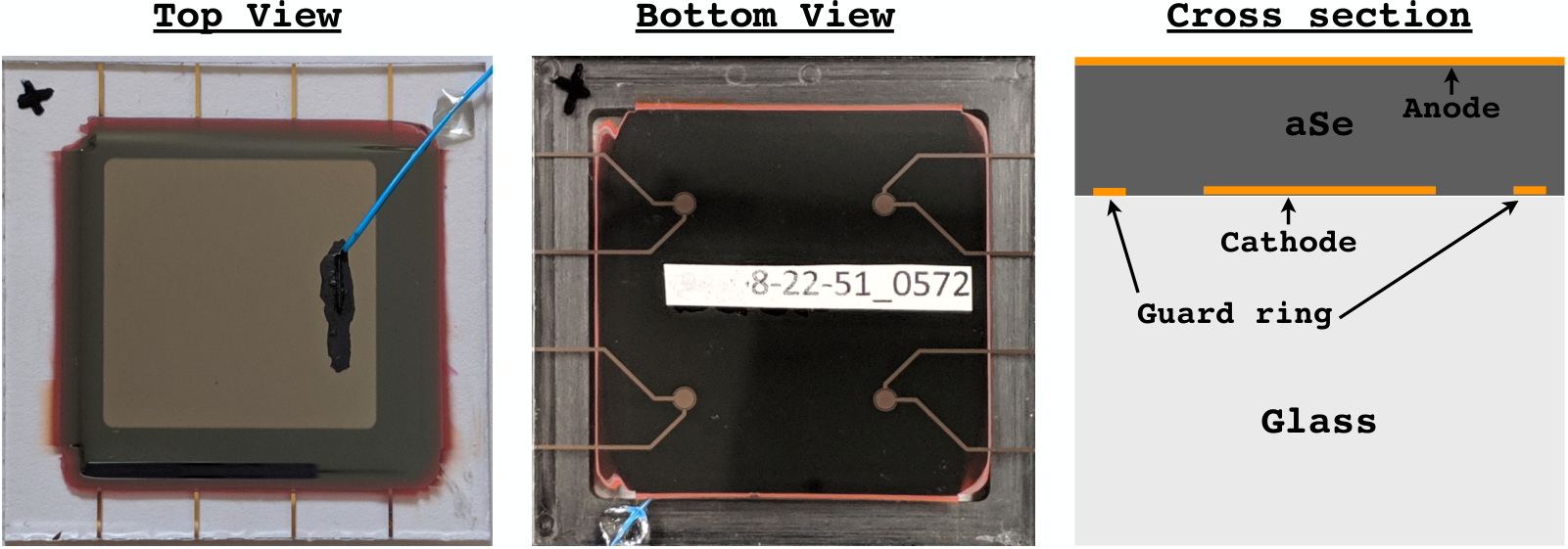
The cathode of the sensor was connected to the CUBE pulse-reset charge sensitive preamplifier with feedback capacitance. The CUBE CMOS chip was glued and wire bonded to a carrier board that was mounted on a plastic holder together with the aSe device. The connection between one of the cathode traces of the aSe device to the input trace of the CUBE carrier board was done by pressing a pin connector soldered on the carrier board firmly onto the trace on the edge of the glass slide. The guard ring was likewise connected to the ground of the carrier board. This method allowed to easily test different aSe sensors while minimizing the input capacitance. The HV connection to the device was done with a single wire fixed on the anode with carbon paint.
A -thick brass collimator with a -diameter hole was mounted above the connected sensor on the device. The collimator was aligned with the sensor by placing a light source below the aSe device and aligning the shadow of the cathode with the hole of the collimator. A 57Co button source of estimated activity at the time of measurement was then taped on top of the collimator. Figure 3 shows the plastic holder with all mounted components.
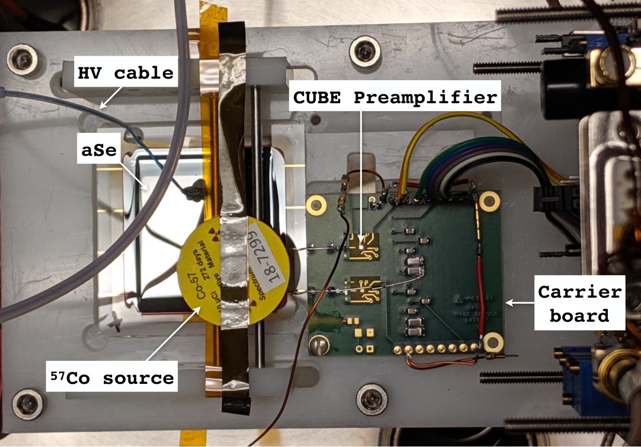
The carrier board of the CUBE was connected with a ribbon cable to an electronics board that amplified the signal, and provided biases and reset pulses to the CUBE. To minimize noise, the CUBE does not have a feedback resistor and its feedback capacitor is instead discharged by a reset pulse generated by the CUBE electronics every time a saturation threshold is reached. Thus, the CUBE acted as an integrator where the output signal was proportional to the charge collected over time, and the frequency of the reset pulses was proportional to the leakage current of the sensor.
The plastic holder with the aSe device, 57Co source, and the CUBE carrier board, as well as the CUBE electronics board, were housed in a vacuum chamber, which was pumped down below so that voltages up to could be applied across the aSe layer without discharges. The vacuum chamber also significantly reduced noise by acting as a Faraday cage to isolate the system from electromagnetic waves, and by stopping sound waves and vibrations that may produce microphonic noise.
A vacuum feedthrough was used to connect to the outside power supply of the electronics board, the HV, and to bring out the signal. The HV was provided by a Stanford Research PS365 power supply. The output signal was capacitively coupled with a high pass filter with time constant to remove the linearly increasing baseline of the CUBE output caused by leakage current. The signal was then fed into a secondary linear amplifier to match the dynamic range of the 12-bit CAEN V740 digitizer, which sampled the signal in digitizer units (ADU) at . The calibration constant of the sampled data was calculated from the specifications of the components in the electronics chain to be /ADU. The digitizer was triggered by a dedicated module whose input was the signal from the secondary amplifier duplicated by a linear fan-in/fan-out unit. The signal was fed to a shaping amplifier and a trigger was generated by a discriminator when the shaping amplifier output was 5 times above the RMS of the baseline level. Because the CUBE reset pulses saturate the secondary amplifier, a gate was opened in response to the CUBE reset to inhibit the trigger for .
Data runs were acquired with HV from in steps. After the HV was increased on the sensor, there was a high leakage current transient that decayed away after several hours. The asymptotic leakage current level was at , increasing with HV to at . Once the sensor was stable, data was acquired continuously for several hours. The shaping time of the amplifier in the trigger module was adjusted for each HV with the aid of an oscilloscope to match the peak time of the signal pulses, which changes due to the different drift time of the free charge in the aSe. Once triggered, the digitizer acquired a time trace in a time window from relative to the trigger time.
3 Ionization signal pulses
The recorded pulses exhibit a oscillation with steady phase and amplitude on the baseline from the switching frequency ripple of the HV power supply, whose amplitude became prominent above and kept increasing with increasing HV. The oscillation was fit and removed from the recorded traces before further analysis. Figure 4 presents examples of the final signal pulses, with a baseline RMS noise of 270 .
The ionization signal starts as soon as the e-h pairs start drifting in the aSe, which induce a current out of the cathode according to Ramo’s theorem. Drifting charges between two parallel planar electrodes generate a current
| (3.1) |
where is the magnitude of the drifting charge, is the applied HV, is the separation between the electrodes, and is the charge-carrier mobility. The output signal is then proportional to the integrated current convolved with the exponential decay constant because the output is capacitively coupled. Thus, the signal may be expressed as
| (3.2) |
where the sum is over the independent contribution to the signal from the drifting electrons () and holes (). is the calibration constant, is the total free ionization charge, and is the mobility of the charge carriers. We define as the time when the ray interacts to generate free e-h pairs in the aSe, while is the time for electrons (holes) to drift to the anode (cathode). Table 1 presents literature values for the charge carrier transport properties of aSe. We do not include in Equation 3.2 the effect of the finite lifetime of the charge carriers in aSe () because it is significantly longer than the maximum carrier drift time. We will revisit the effect of the finite electron lifetime on the measured signal amplitude in Section 4.
| Mobility | Lifetime | Maximum drift time | |
|---|---|---|---|
| at | |||
| Hole | 13-16 | 10-40 | 1.3 |
| Electron | 0.6-0.8 | 40-50 | 30 |
The absorption of rays is not exactly point-like because of the range of the photoelectrons and the emission of fluorescence X rays. However, our particle tracking simulations (see Section 5) show that 84% of the ionization is generated over a range of in depth, which allows us to treat the events as point-like and define the depth of interaction (DOI) as the average perpendicular distance of the ionization event from the anode as a fraction of . The DOI is related to by
| (3.3) | ||||
| (3.4) |
4 Experimental results
Generally, is the addition of the electron and hole signal components (Equation 3.2). However, when the interaction occurs very close to the anode (cathode), () and only the holes (electrons) contribute to the signal. Such pulses can be approximated for by a linear function with the slope proportional to the carrier mobility. Thus, we extract () from the pulses with the minimum (maximum) rise times in our data sample.
Pulses with height within 10% of the full absorption energy of the primary rays were selected and aligned in time such that the start of the pulse is at . The start of the pulse was defined as the intersection between the horizontal line defined by the mean of the baseline and the straight line obtained from the best linear fit to the first five consecutive samples that are above the baseline mean. The baseline mean was subtracted before the pulses were added. Figure 5(a) shows a density plot of all the pulses acquired at , corresponding to a drift electric field .
To construct the average time trace for pulses occurring very close to the anode and cathode, we plot the distribution as a function of time of the pulse trace density along horizontal slices (see Figure 5(b)). For each slice, we consider the time of the pulses with the minimum rise time to occur at the peak delineating the left edge of the distribution, while the maximum rise time is then estimated as the point on the right edge where the density becomes 10% of the plateau level measured after the peak. The average pulses with minimum and maximum rise times are overlaid on the pulse-density plot as yellow circles in Figure 5(a). From a linear fit to the slope of the average pulses we obtain the charge carrier mobilities. Figure 6 shows measured values for as a function of , in agreement with previous measurements [4]. The value for plateaus above because the rise time of the pulses becomes comparable to the digitizer sampling time and, hence, the rise time cannot be measured any more precisely.
With the measured values of , individual ionization pulses were fit with Equation 3.2 to extract the two remaining unknowns and : the amplitude of the ionization signal and the DOI, respectively. Figure 7 shows a two-dimensional histogram of pulse height versus for pulses acquired at . The continuous horizontal band corresponds to the full absorption of the ( emission probability) and ( emission probability) rays from 57Co. Since the aSe thickness is small compared to the attenuation length of the rays, the DOI is evenly distributed across the layer. A fraction of the rays Compton scatter in the aSe, leading to a population of events with uniform DOI that extends to lower energies. Some rays Compton scatter in the collimator, leading to a population of lower energy events at small DOI. Other lower energy photons emitted by the source are below the trigger threshold. The events above the full absorption band may originate from higher-energy rays from 57Co with low emission probability or from environmental radiation, e.g., cosmic rays.
The markers in Figure 7 show the result of a Gaussian fit to the spectrum in space for bins of width 0.05. Figure 8 summarizes the result for different , where the centroid of each band corresponds to the mean peak position and its width the standard deviation (RMS width) returned by the Gaussian fit. The mean peak position increases with increasing because the charge-carrier recombination probability decreases with increasing electric field (see Section 5). Although the peak position should be independent of DOI, we observe that the peak position for a given has a clear maximum at with continuously decreasing values away from this point. We expect a slight decrease in the peak position as a function of because of the finite lifetime of the electrons , which can become comparable to the maximum drift time (see Table 1). Once trapped, the electrons will not contribute to the amplitude of the pulse. A constant should lead to a significant decrease in charge trapping with increasing , since a lower drift time would lead to a smaller trapping probability. However, the fractional decrease in the downward trend past the maximum observed in the data is similar for different . Thus, we were unable to remove the dependence on the peak position by including in our model. One possibility is that the charge trapping probability is not dependent on the charge-carrier drift time but on the distance that the charge carriers travel along the electric field direction.
Generally, almost any observed trend in the peak position can be explained by a corresponding trend in the drift electric field within the aSe. For example, a smaller electric field near the anode could explain the lower peak position at small . The hole blocking layer provides a smooth transition of field strength from zero at the anode to the maximum value in the bulk. Because the hole blocking layer extends into the aSe, ionization events in this region experience greater recombination, as observed at lower . Likewise, fixed space charge within the aSe layer could explain the decreasing peak position toward the cathode. In any case, we do not see any evidence of the aSe layer charging up with time, as we obtain consistent results from data acquired toward the beginning and the end of our longest (12-hour) acquisition run with .
As we do not fully understand the DOI dependence of the full absorption peak, we do not attempt to correct for it and instead select the region (approximately to from the anode) for further analysis. We fit the peak observed in the spectrum to a function with three Gaussian components:
| (4.1) |
where is the mean energy required to produce one free e-h pair in aSe, and account for the full absorption of the rays and its corresponding K escape line at , and accounts for the full absorption of rays. We use a common for the RMS width of the three lines and constrain their relative intensities to the ratios . The 10% K X ray escape probability was obtained from a Geant4-based particle-tracking simulation that includes the detailed detector geometry (see Section 5). The fit range was chosen as to avoid the lower energy tail of events from Compton scattering. Figure 9 presents the measured spectra at different with the overlaid best-fit line.
5 Ionization response of amorphous selenium
To better understand the measured spectrum we developed a full detector simulation, including the microphysics of recombination in aSe. The simulation is based on Geant4 [5], which tracks all particles and simulates all interactions starting with the emitted rays from the source, followed by transport through the collimator and the device structure, the photoabsorption in the aSe layer, and the energy depositions by the ionizing electrons. The simulation adopts the Penelope low energy physics that includes atomic relaxation processes [6]. For every energy deposition, we simulated the generation of free charge that drifts to the electrodes and gives rise to a signal pulse according to the model in Section 3. We introduced the baseline noise from the pre-trigger window in the data on the simulated pulses, and applied a digital low-pass filter with time constant . We performed the same signal extraction procedure on the simulated pulses as in the data to obtain the total pulse charge for each event and generate simulated spectra from the source. Our detector simulation shows that our fitting procedure to the pulses successfully recovers independent of with an uncertainty from electronic noise and the signal extraction procedure of . This uncertainty contributes to the measured RMS width of the photabsorption lines as , where is the contribution from fluctuations in charge generation in aSe.
For our charge-generation model, we set the ionizing electron step size in the aSe layer and the requirement to generate secondary electrons in Geant4 to their minimum values to best capture the fluctuations in the deposited-energy density along the track and to account for the large discrete energy depositions by low-energy secondary electrons. We take every step as a -long straight track segment and further divide it into subsegments of length , where the “spur size” 1–5 depends on the kinetic energy of the electron at the beginning of the step. We take to be proportional to the function in Figure 8 of Ref. [7] with scaling constant as a variable in our model. The energy deposited by an ionizing electron in a step is calculated by Geant4 from a discrete number depositions of energy , where is determined by the mean free path of the electron as a function of , and follows a probability distribution proportional to [8, 9]. We extracted these discrete energy depositions from Geant4 and distributed them randomly and uniformly along the step, adding the initial ionization charge from each energy deposit to the corresponding subsegment. The initial ionization charge was calculated as , where the energy required to generate an e-h pair in aSe 4–7 [10, 11] is a variable in our model. For each subsegment, we follow the box recombination model from Ref. [12] to calculate the average free charge that survives recombination assuming that the initial ionization charge is distributed uniformly within a cylindrical volume of length and radius :
| (5.1) |
For the recombination coefficient , we adopt the modified expression proposed for aSe in Ref. [13]:
| (5.2) |
with and the permittivity of aSe [14, 13], where is the vacuum permittivity. In Equations 5.1 and 5.2, corresponds to the sum of the mobilities of the charge carriers, which in aSe can be approximated as measured in Section 4. For every track subsegment, we assume that charge is generated, drawn from a Poisson distribution with mean . Following the complete detector simulation, we obtained predicted spectra for different values of , and recombination model parameters and .
Figure 10 presents an example of the predicted energy spectrum from our simulation. The dominant contribution to the width of the full absorption peak comes from the dependence of the recombination probability on the deposited-energy density along the ionizing-electron tracks. The figure also shows the predicted spectrum if the recombination probability were to be constant and uncorrelated for every generated e-h pair, exhibiting a much better energy resolution capable of resolving the three separate spectral lines. The amplitude of the low-energy tail on the left-hand side of the peak is larger in the data than in the simulation possibly because the alignment of the collimator is more accurate in the simulation than in the real experiment. The cutoff in the energy spectrum for is caused by the trigger threshold, which is well reproduced by the electronics simulation.
Figure 11 summarizes the measured values of and , the fractional energy resolution at , as a function of . These two parameters are the most relevant to understand the energy response of aSe. The value of decreases with increasing because of the decrease in the fraction of primary e-h pairs that recombine. This trend was observed in past measurements [13], although the reported absolute values of at a particular appear to vary from sample to sample depending on the specific composition of the aSe layer [15]. The observed energy resolution is comparable to past measurements with X rays [16]. From our simulations, we obtain predicted curves for as a function of and . From a fit to the data shown by the red line in Figure 11(a), we obtained best-fit values and . The corresponding prediction for is shown by the red line in Figure 11(b), in satisfactory agreement with data.
6 Implications for neutrinoless decay search
The recombination model presented in Section 5 provides a framework to estimate the energy resolution of aSe to events from the neutrinoless decay of 82Se. We extended the size of the aSe target layer in our Geant4-based simulation to fully contain pairs of electrons from neutrinoless decay. Starting from the initial kinetic energy distributions provided by the Decay0 program [17], we simulated the ionizing electron tracks and the corresponding charge generation and recombination processes. From the distribution of the total free charge produced in each event, we obtain an energy resolution at of 2.8% for . This result is significantly larger than the 0.34% estimated in Ref. [1]. Our simulation predicts that increasing the drift electric field could further improve the energy resolution to 2.0% at . Further, because fluctuations in ionization density are correlated with straggling of the electrons, the average charge yield for an electron track is anti-correlated with its length. Hence, if the track length could be accurately measured (as in the detector proposed in Ref. [1]), with a simple first-order linear correction the resolution could be improved to 1.1%.
Note that our recombination model has only been validated with electrons from the photoabsorption of rays from a source, while the electrons emitted by decay are an order of magnitude more energetic. In particular, the deposited-energy density is significantly lower along the tracks of higher-energy electrons, an unexplored regime where we expect a smaller charge recombination probability. The experimental technique used for this measurement cannot be extended to electrons of much higher energy because above rays primarily Compton scatter, generating multiple low-energy electrons, and the few high-energy electrons from photoelectric absorption escape the aSe target because of their long range. We are fabricating larger hybrid aSe/CMOS imaging sensors in area with -thick aSe layers that can fully contain higher-energy electrons. These devices will allow us to measure the charge yield as a function of deposited-energy density for a better understanding of the ionization response of aSe. Furthermore, we expect to improve the energy resolution by correcting for the difference in charge yield along the imaged electron tracks. Beyond simple analytical corrections, this problem is particularly well suited for machine learning approaches [18, 19] given the wealth of information encoded in the high-resolution electron tracks. Ultimately, we aim to implement a detailed ionization response model and energy reconstruction procedure in a realistic simulation of the detector proposed in Ref. [1] to accurately evaluate its prospects in the search for neutrinoless decay.
Acknowledgments
This material is based upon work supported by the U.S. Department of Energy, Office of Science, Office of Nuclear Physics Fundamental Symmetries program under Award Number DE-SC-0020439.
References
- [1] A. E. Chavarria, C. Galbiati, X. Li and J. A. Rowlands, A high-resolution CMOS imaging detector for the search of neutrinoless double decay in 82Se, J. Instrum. 12 (2017) P03022.
- [2] S. Dell’Oro, S. Marcocci, M. Viel and F. Vissani, Neutrinoless Double Beta Decay: 2015 Review, Adv. High Energy Phys. 2016 (2016) 2162659.
- [3] M. D. Tabak and P. J. Warter, Field-controlled photogeneration and free-carrier transport in amorphous selenium films, Phys. Rev. 173 (1968) 899.
- [4] G. Juška and K. Arlauskas, Impact ionization and mobilities of charge carriers at high electric fields in amorphous selenium, Phys. Status Solidi A 59 (1980) 389.
- [5] J. Allison, K. Amako, J. Apostolakis, P. Arce, M. Asai, T. Aso et al., Recent developments in GEANT4, Nucl. Instrum. Methods Phys. Res. A 835 (2016) 186.
- [6] D. N. Abdurashitov, Y. M. Malyshkin, V. L. Matushko and B. Suerfu, Response of a proportional counter to 37Ar and 71Ge: Measured spectra versus Geant4 simulation, Nucl. Instrum. Methods Phys. Res. B 373 (2016) 5.
- [7] E. Fourkal, M. Lachaine and B. G. Fallone, Signal formation in amorphous-Se-based x-ray detectors, Phys. Rev. B 63 (2001) 195204.
- [8] K. Lassila-Perini and L. Urbán, Energy loss in thin layers in GEANT, Nucl. Instrum. Methods Phys. Res. A 362 (1995) 416.
- [9] Geant4 collaboration, “Energy Loss Fluctuations — Physics Reference Manual 10.4 documentation.” http://geant4-userdoc.web.cern.ch/geant4-userdoc/UsersGuides/PhysicsReferenceManual/BackupVersions/V10.4/html/electromagnetic/energy_loss/fluctuations.html#em-straggling-bichsel. Accessed: 2020-10-10.
- [10] W. Que and J. A. Rowlands, X-ray photogeneration in amorphous selenium: Geminate versus columnar recombination, Phys. Rev. B 51 (1995) 10500.
- [11] C. A. Klein, Bandgap dependence and related features of radiation ionization energies in semiconductors, J. Appl. Phys. 39 (1968) 2029.
- [12] V. Cataudella, A. De Candia, G. D. Filippis, S. Catalanotti, M. Cadeddu, M. Lissia et al., Directional modulation of electron-ion pairs recombination in liquid argon, J. Instrum. 12 (2017) P12002.
- [13] O. Bubon, K. Jandieri, S. D. Baranovskii, S. O. Kasap and A. Reznik, Columnar recombination for X-ray generated electron-holes in amorphous selenium and its significance in a-Se x-ray detectors, J. Appl. Phys. 119 (2016) 124511.
- [14] M. Lachaine and B. G. Fallone, Monte Carlo simulations of x-ray induced recombination in amorphous selenium, J. Phys. D: Appl. Phys. 33 (2000) 1417.
- [15] S. O. Kasap, K. V. Koughia, B. Fogal, G. Belev and R. E. Johanson, The influence of deposition conditions and alloying on the electronic properties of amorphous selenium, Semiconductors 37 (2003) 789.
- [16] I. M. Blevis, D. C. Hunt and J. A. Rowlands, Measurement of x-ray photogeneration in amorphous selenium, J. Appl. Phys. 85 (1999) 7958.
- [17] O. A. Ponkratenko, V. I. Tretyak and Y. G. Zdesenko, Event generator DECAY4 for simulating double-beta processes and decays of radioactive nuclei, Phys. At. Nucl. 63 (2000) 1282.
- [18] P. Ai, D. Wang, G. Huang and X. Sun, Three-dimensional convolutional neural networks for neutrinoless double-beta decay signal/background discrimination in high-pressure gaseous Time Projection Chamber, J. Instrum. 13 (2018) P08015.
- [19] J. Liu, J. Ott, J. Collado, B. Jargowsky, W. Wu, J. Bian et al., Deep-Learning-Based Kinematic Reconstruction for DUNE, 2012.06181.