Accessing the spectral function of in operando devices by angle-resolved photoemission spectroscopy
Abstract
Progress in performing angle-resolved photoemission spectroscopy (ARPES) with high spatial resolution in the order of 1 m or less (nanoARPES) has opened the possibility to map the spectral function of solids on this tiny scale and thereby obtain detailed information on the materials’ local electronic band structure and many-body interactions. Recently, nanoARPES has been used to study simple electronic devices, based on two-dimensional materials, with the possibility of tuning the carrier type and density by field effect-gating, and while passing a current through the device. It was demonstrated that nanoARPES can detect possible changes in the materials’ electronic structure in these situations and that it can map the local doping, conductance and mobility. This article reviews these first in operando ARPES results on devices, discusses the resulting new insights, as well as the perspectives for future developments of the technique.
I Introduction
Angle-resolved photoemission spectroscopy (ARPES) is an experimental approach to study the electronic properties of crystalline solids. ARPES is a sophisticated version of the photoelectric effect and was first developed in the 1970’s and 80’s. Initially, the main aim was to study the occupied band structure of solids but it was soon discovered that information about many-body effects such as electronic correlations or the electron-phonon interaction could be investigated as well. ARPES has seen an enormous technical improvement after the discovery of high-temperature superconductivity, as it was thought to be the technique of choice to characterise the interactions leading to this phenomenon.
Over the last 40 years, ARPES experiments have almost exclusively been performed on nominally uniform millimetre-sized single crystals (the crystal has to be larger than the diameter of the UV light spot used for photoexcitation) Plummer and Eberhardt 1982; Kevan 1992; Hüfner 2003; Damascelli et al. 2003; Hofmann et al. 2009; Lu et al. 2012; Sobota et al. 2020. Only very recently, it has become possible in an ARPES context to focus the UV light to a spot size of less than a few m, opening the possibility to study a variation of electronic phenomena on this scale, as well as to map a sample’s electronic structure by scanning the UV beam across its surface Rotenberg 2010.
The high spatial resolution can also be exploited to study samples that were hitherto not accessible to ARPES, for example simple electronic devices made of two-dimensional (2D) materials such as graphene or single-layer MoS2. Typically, such a device is built up as a field effect transistor, permitting the control of the carrier concentration in the 2D material via a gate voltage. The 2D material channel is only a few m wide and it is thus extremely demanding to focus the UV spot on this channel only. Indeed, such systems cannot be studied using a standard ARPES beamline and the exploration of devices by ARPES has only become possible due to the aforementioned recent progress in focusing the UV beam to a size much smaller than the typical device dimensions. This review describes the first ARPES experiments on such devices in operando i.e., while the 2D material is exposed to gate fields and currents.
The application of electric fields to a material may not only lead to a modified carrier density and electric currents, but potentially also alter many-body effects or even induce phase transition, e.g., from a Mott insulator to a conductor. The so-called “quantum materials” (QMs) are particularly prone to such transitions and the recent development of ARPES performed on devices opens the door to studying the electronic structure and many-body effects of QMs in field-induced states – information that was previously inaccessible.
We briefly discuss why the application of electric fields and currents, along with many other tuning parameters such as strain, pressure and chemical composition, is particularly interesting in the context of QMs. We start with the question: What are QMs? At present, there is no agreed-upon definition of what constitutes a QM. There is, however, broad agreement that QMs are typically characterised by strong electronic correlations or topological band structures, often combined with reduced dimensionality Keimer et al. 2015; Keimer and Moore 2017; Basov et al. 2017; Tokura et al. 2017. QMs feature extraordinary properties, such as high-temperature superconductivity and exotic quantum Hall effects. The field of QM research has evolved from the interest in correlated electronic materials but the class of QM now also contains materials that can be well-described by single-particle band structures, for example the Bi2Se3 group of topological insulators.
The state of many QMs is controlled by a subtle balance between different interactions of similar strength. This leads to so-called “emergent phenomena” that arise due to the interplay of these interactions, entailing the QM with new properties. Moreover, a small stimulus can often be used to upset the ground state equilibrium and “switch” the QM between radically different states—e.g., from insulating to superconducting. Quantum phase transitions (not involving temperature) are a common phenomenon in these materials Vojta 2003 and so is the spontaneous spatial separation between coexisting different phases. Pushing QMs out of equilibrium can even give rise to entirely new forms of quantum matter Wang et al. 2013; Rudner and Lindner 2020.
Understanding and exploiting phase transitions in QMs is one of the major challenges in contemporary condensed matter physics. Much interest has been directed towards driving phase transitions in QMs by a range of stimuli such as ultrafast laser excitations Cavalleri et al. 2001; Schmitt et al. 2008; Rohwer et al. 2011; Fausti et al. 2011; Wang et al. 2013; Mitrano et al. 2016; Caputo et al. 2018, or simply the application of electric fields or DC currents Taguchi et al. 2000; Lee et al. 2007; Vaju et al. 2008; Monceau 2012; Stoliar et al. 2013; Nakamura et al. 2013; Rudner and Lindner 2020; Bellec et al. 2020. An illustration of this is given in Figure 1 which shows a generic phase diagram of a QM as a function of an applied electric field and consequently a current density in the case of a conductive material, as well as an additional control parameter . could be the sample temperature, for example in the case of insulator-to-metal transition in the Mott insulator Ca2RuO4 Nakamura et al. 2013; Bertinshaw et al. 2019; Cirillo et al. 2019; Zhang et al. 2019; Mattoni et al. 2020 but it could also be some other control parameter. For Ca2RuO4, this could be chemical composition Nakatsuji and Maeno 2000 (substitution of Ca by Sr), pressure Nakamura et al. 2002 or strain Riccò et al. 2018; Sunko et al. 2019. In fact, for many QMs the corresponding phase diagram is likely to be multi-dimensional.
We highlight here the role of electric field and current-driven phase transitions in QMs because, in a practical device setting, electric fields are much easier to administer than, e.g., magnetic fields, strain or hydrostatic pressure. There is a large number of examples for current-driven transitions, such as sliding of charge density wave condensates, insulator-to-metal transitions in Mott insulators, the current-induced breakdown of superconductivity or field-induced changes in band topology Taguchi et al. 2000; Lee et al. 2007; Vaju et al. 2008; Monceau 2012; Stoliar et al. 2013; Nakamura et al. 2013; Rudner and Lindner 2020; Bellec et al. 2020. We stress that, with respect to applications of QMs in electronic devices, such phenomena imply that the QM’s role in a device can be completely different from, e.g., silicon: Whereas an electric current leaves the properties of a normal material unaltered, it has the potential to change the state of some QMs, something that is not exploited in conventional electronic devices.
The electronic structure of a material – and its modification as a function of some external parameter or across a phase transition – is closely related to its electrical transport properties. Transport measurements can be performed over a wide range of temperatures, in strong magnetic fields, for strained samples or during the exposure to light. While the primary quantity measured is the electrical conductivity of the sample, the simultaneous application of magnetic fields can give detailed information about the carrier density, the carrier’s effective mass, the Berry phase, the presence of weak (anti)-localisation, quantum transport through edge states and many other phenomena. Magneto-transport measurements have therefore been of key-importance in the characterisation of solids for many years Ashcroft and Mermin 1976.

Ultimately, the transport properties and the complete electronic structure of a solid are encoded in its spectral function . In a simple picture, can be viewed as the probability of finding an electron with energy and wave vector . In a system of non-interacting electrons (not typically a good approximation in QMs), has the character of a -function at the energy and values given by the single particle dispersion . This changes when interactions are turned on. In the simplest situation described by a so-called quasiparticle picture, the maxima in are broadened and shifted away from . For very strong many-body interactions, the quasiparticle picture might even break down. This is reflected in more complex structures in that are not related to in a simple way. Regardless, the spectral function is often proportional to the photoemission intensity observed in ARPES, so that the complex many-body interactions can be tracked by this technique.
While ARPES has been extensively used to study QMs in equilibrium Damascelli et al. 2003; Keimer et al. 2015; Lu et al. 2012, its applicability to phenomena driven by external parameters, such as in Figure 1, can be restricted because such parameters need to be reconciled with the requirements of performing electron spectroscopy in ultra-high vacuum. While it is trivial to change the chemical composition by using different samples, and relatively simple to change the temperature using a cryostat, at least down to a few K, some highly interesting experimental conditions are difficult or even impossible to explore. The presence of electric and magnetic fields, for instance, is highly problematic because these change the trajectory of the photoemitted electrons. Also, hydrostatic pressure cannot be applied because the path of the photoelectrons to a detector is blocked in a diamond anvil cell. On the other hand, there has been recent progress with parameters such as strain to tune QMs and to trigger phase transitions while investigating the electronic structure using ARPES Riccò et al. 2018; Flötotto et al. 2018; Lin et al. 2020.
ARPES with spatial resolution, the key technique for this review, is often called micro ()-ARPES or nanoARPES. For simplicity, we will not make this distinction here and just refer to the technique as nanoARPES. NanoARPES opens many interesting opportunities for the study of QMs because it not only gives access to intrinsically small samples but potentially also to phenomena such as phase separation in QMs and otherwise inhomogeneous systems. Indeed, while nanoARPES is a relatively recent technique, it has already given rise to a number of important results Rotenberg 2010; Noguchi et al. 2019; Kastl et al. 2019; Ulstrup et al. 2019a; Utama et al. 2020; Lisi et al. 2020; Ulstrup et al. 2020. Here we focus on the possibility to determine the spectral function of a QM in electronic devices in the presence field-induced doping and / or a finite current density. As we shall see, this opens a spectroscopic window on many phenomena that are usually inaccessible to ARPES investigations. Most importantly in connection with QMs, it should allow unique new insights in the modification of the materials’ spectral function upon doping and under current-induced phase transitions.
In addition to accessing the non-equilibrium spectral function of a QM in an operating device, we shall see that nanoARPES on current-carrying devices permits a contact-free mapping of the local potential, such that the spectroscopic measurements are accompanied by a transport measurement. This bridges the gap between the usually disparate fields of ARPES and transport measurements and it allows to link transport properties such as the local conductivity or mobility to local structural features in the investigated QM.
The advent of nanoARPES is only one of the necessary ingredients for mapping the spectral function in operating devices. As we shall see, ARPES is a very surface-sensitive technique and mapping the spectral function of a deeply buried conductive channel in a conventional silicon field effect transistor or a quantum Hall effect device would be extremely challenging. Therefore, other important conditions for the research reported here have been the discovery of (and the continued interest in) 2D materials, as well as the development of techniques that permit the construction 2D materials-based devices suitable for nanoARPES investigations. Indeed, there are several other experimental constraints that have so-far limited nanoARPES studies of functional devices to very simple situations involving 2D materials. The surface-sensitivity of the technique, for instance, does also imply that an atomically clean surface is required for nanoARPES investigations, along with need to place the sample in ultra-high vacuum for the surface to remain clean for an extended period of time. There are several other formidable experimental challenges that have so-far prohibited nanoARPES studies on many interesting nano-scaled devices exhibiting superconductivity, magnetism or spin-selection. These experimental constraints will be discussed in detail.
This review is structured as follows: Following this introduction, section II will describe the necessary technical ingredients enabling the in operando study of QM-based devices. These are 2D (mainly) QMs, nanoARPES, and 2D QM-based devices compatible with the requirements for nanoARPES. Section III illustrates how the spectral function can be mapped across a device in equilibrium and what kind of information can be obtained from such a measurement. Section IV reviews results obtained from field-doping 2D devices using a gate voltage. Section V describes the use of nanoARPES in the presence of a steady state current. Section VI discusses experimental challenges for nanoARPES on devices. Section VII is an extended outlook on future developments of the technique. The review is ended by a brief conclusion in Section VIII.
II Experimental considerations
II.1 Two-dimensional quantum materials
Low dimensionality is a frequently encountered feature of QMs, even if the materials are not outright 2D or one-dimensional (1D). Important examples of (quasi) 2D electronic systems arise in the integer Klitzing et al. 1980 and fractional Tsui et al. 1982 quantum Hall effects, the quantum spin Hall effect Konig et al. 2007, the cuprate superconductors Bednorz and Müller 1986 and numerous CDW materials Grüner 1994. As we shall see below, ARPES is especially well-suited for determining the electronic structure of 2D electronic systems. On the other hand, it is a very surface-sensitive technique and this precludes access to the buried two-dimensional electron gas (2DEG) in a typical quantum Hall effect device or a metal oxide field effect transistor. The advent of 2D materials has been an essential condition for in operando ARPES studies on devices because these materials can be placed right at the surface of the device. However, it should be mentioned that band bending-induced 2DEGs can also exist near the surfaces of many semiconductors and insulators and these have been studied by ARPES (see e.g. King et al. 2010; Bianchi et al. 2010; Santander-Syro et al. 2011; Meevasana et al. 2011; Kim et al. 2015).
The successful fabrication of 2D materials Novoselov et al. 2005 was heralded by the discovery of graphene Novoselov et al. 2004; Zhang et al. 2005 and the devices that are typically fabricated for transport experiments on such materials are already very close to meeting the requirements for being studied with surface-sensitive techniques such as ARPES. The field of 2D materials is vast and many excellent reviews about particular aspects and classes of materials are available Neto et al. 2009; Kara et al. 2012; Basov et al. 2014; Das et al. 2015; Avouris et al. 2017; Manzeli et al. 2017; Dong and Kuljanishvili 2017; Zhao and Jia 2020; Andrei and MacDonald 2020. We therefore only mention the most relevant 2D QMs for the use in ARPES investigations of in operando devices.
The vast majority of 2D materials is derived from layered bulk materials with weak van der Waals bonding between the layers but there are some for which this is not the case, such as silicene Kara et al. 2012 and stanene Zhao and Jia 2020, and some do not even have a bulk counterpart of the same chemical composition Arnold et al. 2018. Single or few-layered 2D materials can often be extracted from their layered bulk counterpart by mechanical exfoliation and assembled into functional devices Avouris et al. 2017. The most important material classes in this context are graphene Neto et al. 2009; Basov et al. 2014 and the few-layer transition metal dichalcogenides (TMDCs) of the MX2 type (and from this class mostly the semiconducting and more inert compounds, such as MoS2 Manzeli et al. 2017; Dong and Kuljanishvili 2017). Simple field effect transistor-based devices made from these materials have been at the heart of studying their transport properties Novoselov et al. 2004; Zhang et al. 2005; Radisavljevic et al. 2011 and have illustrated many fascinating properties, such as the unconventional Hall effect for graphene Novoselov et al. 2004; Zhang et al. 2005, the transition from a semiconductor to a superconductor in single layer (SL) MoS2 Costanzo et al. 2016, as well as a metal-insulator transition driven by electronic correlations in the same material Radisavljevic and Kis 2013. Another very important 2D version of a layered compound is thin hexagonal BN (-BN). In fact, this highly insulating and inert material has a central role in 2D materials devices. It is almost ubiquitously used as a protective layer or a gate dielectric and is the key to achieving ultra high mobility in graphene devices Dean et al. 2010. Its importance for 2D material-based devices can hardly be overstated Watanabe et al. 2004.
Currently, the main focus of 2D QMs research is no longer on SL materials, but on several such layers stacked on top of each other into heterostructures Geim and Grigorieva 2013; Novoselov et al. 2016. Naively, one could expect such stacks to inherit the properties of the individual layers but it turns out that this simple picture can break down, giving rise to combined materials with emergent properties. Examples for this are the formation of atomically thin junctions Cheng et al. 2014, hybridisation between 2D layers Wilson et al. 2017; Zribi et al. 2019, as well as proximity effects (magnetic, spin-orbit, superconducting) Avsar et al. 2014; Li et al. 2020; Lüpke et al. 2020; Žutić et al. 2019. Also, the exact stacking angle in a bilayer of 2D materials turns out to be an important tuning parameter for the combined system’s properties. A particularly simple model system is twisted bilayer graphene Andrei and MacDonald 2020 which, depending on the twist angle, shows properties that are very different from those of the SL or the (usual) Bernal stacked bilayer, such as strong electronic correlations leading to an insulating state Cao et al. 2018a or, upon slight electrostatic doping, superconductivity Cao et al. 2018b. Remarkably, both phenomena occur for twist angles close to a so-called “magic angle” of . This can be understood in terms of a long range moiré pattern forming at this twist angle, resulting in a very small Brillouin zone. Hybridisation between the graphene sheets gives rise to nearly flat bands near the Fermi level throughout this Brillouin zone. The flat bands, in turn, lead to a high density of states and strong correlations. Note, however, that such phenomena can only be realised for a very accurate tuning of the twist angle and at low temperatures.
The functional devices investigated by nanoARPES so far have been built from graphene, TMDCs or combinations of these materials, always also using thin layers of -BN. An important reason for the choice of these materials was the ease with which these can be handled, their high stability and chemical inertness, which results in devices with reasonably clean surfaces, and the recent progress in assembling these materials with unprecedented controll and precision Frisenda et al. 2018. There is no reason why in principle devices for nanoARPES could not be extended to other classes of 2D materials Haastrup et al. 2018, for example 2D topological materials Hou et al. 2020, stanene Zhao and Jia 2020 or bismuthene Reis et al. 2017. Indeed, several of the ideas used for 2D materials could also be explored for the 3D QMs discussed in the introduction. Electrostatic gating of 3D QMs is difficult unless they are non-metallic and very thin but exploring their response to a high current density close to the surface should be possible.
II.2 Angle-resolved photoemission on the nano-scale
II.2.1 Very brief introduction to ARPES
Angle-resolved photoemission spectroscopy is an experimental technique based on the photoelectric effect. It was developed in the 1970s to study the band structure of solids, building on tools developed for X-ray photoemission spectroscopy. First studies of many-body effects such as the electronic self-energy were also reported in the 1980s (see e.g. Ref. Jensen and Plummer 1985). The technique saw an enormous improvement of instrumentation Mårtensson et al. 1994 following the discovery of high-temperature superconductivity Bednorz and Müller 1986, since it promised a direct view on how many-body interactions would manifest themselves in the spectral function. Indeed, the large energy scale for high-temperature superconductivity ( meV Lanzara et al. 2001) meant that relevant many-body effects were within reach of realistic energy resolution targets. Today, it is possible to achieve energy and angular resolutions better than 1 meV and 0.1∘ Kiss et al. 2008, as well as sample temperatures below 1 K Borisenko 2012, opening the possibility to study even conventional superconductivity.
There are many excellent reviews and books published on ARPES (for a selection see Refs. Plummer and Eberhardt 1982; Kevan 1992; Hüfner 2003), even on more specialised issues such as ARPES on cuprate superconductors Damascelli et al. 2003, quantum materials Lu et al. 2012; Sobota et al. 2020, the use of high photon energies Suga and Tusche 2015; Strocov et al. 2019, the electron-phonon interaction Hofmann et al. 2009 and ARPES for the investigation of many-body effects on the nano-scale Rotenberg 2010. We therefore only summarise some of the most basic concepts here, aiming for an easily accessible level.
Figure 2(a) illustrates the basic idea of ARPES. The surface of a material is exposed to monochromatic UV photons with an energy exceeding the sample’s work function , resulting in the emission of photoelectrons with a kinetic energy of
| (1) |
where is the electrons’ binding energy, measured with respect to the Fermi energy of the sample. The measured of a spectral feature is the quantity of interest when considering the (single particle) band structure of the solid, . can be calculated using equation (1) or directly read from the photoemission spectra because is often clearly identifiable as a sharp intensity change (if the sample is not metallic, a metal in contact with the sample can be used for this energy calibration). Note that ARPES data is often displayed as a function of and a positive binding energy but is also common to instead use the negative energy difference .
While energy conservation is thus straight-forward, momentum conservation is not. The outgoing photoelectron has a momentum of and the three dimensional is completely determined by the measurement of the kinetic energy and the emission angles and in Figure 2(a). The difficulty lies in working back to inside the solid. The 2D component of parallel to the surface, , is conserved in the photoemission process because the system retains its translational symmetry parallel to the sample surface, so
| (2) |
modulo a 2D (surface) reciprocal lattice vector. For the component perpendicular to the surface, , the situation is more complicated. The translational symmetry in this direction is broken and is no longer a good quantum number. It is also poorly defined because the electrons of interest, those which escape the solid without inelastic scattering, stem from a region very close to the surface (see below), giving rise to a well-defined position and a therefore poorly defined (crystal) momentum . Nevertheless, determinations of the 3D band structure of a solid are often possible by varying via changing the photon energy. Fortunately, none of this is relevant for studying the (quasi) 2D materials we focus on here. For a 2D material, is the only relevant quantum number and the described procedure yields the desired initial state band structure .
A band structure determination along these lines is illustrated for the valence band of a SL of MoS2, a 2D material, in Figure 2(b) Miwa et al. 2015. The greyscale image shows the photoemission intensity as a function of , following the red path in the inset of the figure, and the binding energy. The zero of the binding energy scale at is easily identified by the step-like change of the intensity. This is due to the fact that the SL MoS2 is placed on a metallic gold substrate. The valence band is also clearly seen by an increased intensity, leading to particularly sharp features in the vicinity of the K point in the Brillouin zone. For comparison, the calculated dispersion for the valence band of free-standing SL MoS2 is shown as a red line superimposed on the photoemission intensity.

A very important consideration in ARPES is the high surface sensitivity of the experiment that stems from the short inelastic mean free path of the excited photoelectrons in matter. Figure 3 shows the inelastic mean free path for some materials as a function of energy, along with a calculation for the free-electron model Penn 1976 (dashed line). Since this calculation represents the typical behaviour for many solids, the curve is often referred to as the “universal curve” for the electron inelastic mean free path but it needs to be noted that deviations from this generic behaviour have to be expected, in particular at low energies. The inelastic mean free path is rather short for all kinetic energies and especially for the energies most relevant to ARPES (between 10 and a 100 eV); the electrons that have escaped the solid without undergoing inelastic scattering processes are thus likely to stem from the first few layers of the material. Only these electrons are relevant for extracting band structure information in ARPES since information on the initial state energy and is lost in an inelastic scattering process.
The short inelastic mean free path imposes some important restrictions on ARPES experiments in general and ARPES on devices in particular. All ARPES experiments are very surface-sensitive, implying that atomically clean surfaces are required for the measurements. This, in turn, calls for approaches to obtain clean surfaces, such as the cleaving of bulk crystals, combinations of noble gas sputtering and thermal annealing or the use of very inert surfaces that do not need extra cleaning. Also, the surfaces need to remain clean during the time of the experiments. This requires carrying out ARPES experiments in ultra-high vacuum, i.e. at a pressure well below 1 mbar. For ARPES experiments on devices, the short inelastic mean free path of the electrons also prevents spectroscopy on interfaces that are deeply buried under thick protective layers or top-electrodes for gating (approaches to circumvent this problem are discussed in Section VII).

The above considerations explain how ARPES can be used to measure the single particle band structure of crystalline materials but the enormous significance of the technique in modern condensed matter physics stems from the fact that it also opens a window onto the many-body effects governing the behaviour of complex QMs. In order to understand this, a slightly more advanced picture of the photoemission process is needed. Still in a simplified picture, and ignoring effects of finite energy and angular resolution, the measured photoemission intensity is given by
| (3) |
where is the dipole matrix element for the excitation from initial state to final state in the photoemission process, is the Fermi-Dirac function ensuring that only occupied states can contribute to the photoemission intensity, and is the desired spectral function. We assume that the sample is a 2D material and is a 2D vector. The matrix element for an initial state of given symmetry can strongly depend on parameters such as the photon energy or the light polarisation. However, when investigating the spectral function over a small range of , the -dependence of the matrix elements is often negligible.
The spectral function describes the electronic structure of a solid in the presence of many-body effects. can be viewed as the probability of finding an electron with energy and momentum at a given temperature . From now on, we drop the explicit reference to in the notation for convenience. In a quasiparticle picture, where the many-body interactions do not lead to a complete breakdown of the band structure idea but merely to the picture of quasiparticles instead of non-interacting electrons, can be stated in terms of the “bare” dispersion for non-interacting electrons and the complex self-energy . It is usually assumed that is independent of . Then has the form
| (4) |
where and are the real and imaginary parts of the self-energy.
A somewhat simplified interpretation of in the form of equation (4) is that the many-body effects, as encoded in , lead to a spectral function that resembles that of the bare dispersion with two important modifications: Instead of being a -function tracking , the dispersion is broadened by , the imaginary part of and shifted by , the real part. The simplest situation is that of an energy-independent scattering mechanism, for example defect scattering. In this case, is independent of energy and given by and The resulting spectral function is shown in Figure 4(a). The bare dispersion is given by the solid line and the maximum in the spectral function tracks this line. The broadening corresponds to the quasiparticle now having a finite lifetime due to scattering and this lifetime is given by . In this simple case, the interpretation of the ARPES features tracking the single particle band structure is valid. The many-body effects merely lead to a broadening but do not affect the dispersion as such.

The situation of a more complicated interaction with a bosonic mode (e.g., a phonon) is illustrated in Figure 4(b). Here the dispersion changes in the vicinity of . The position of the crossing, , remains the same but the dispersion flattens out near , leading to an increased effective mass of the quasiparticle which now is a mixture of an electron and a phonon. This is accompanied by a characteristic “kink” at a higher binding energy corresponding to the energy of the phonon. Such kinks are often observed in the case of systems with strong electron-boson coupling Hengsberger et al. 1999; Valla et al. 1999a; Lanzara et al. 2001; Hofmann et al. 2009.
The analysis of a measured spectral function should ideally yield the bare dispersion , as well as the complex self-energy . Extracting these quantities is not trivial since is usually not known. Commonly, 1D cuts through the spectral function are analysed, either at constant (so-called energy distribution curves) or at constant (so-called momentum distribution curves). The latter approach has the advantage that, within the approximation of equation (4) and assuming a locally linear dispersion, the momentum distribution curve can be described by a Lorentzian Valla et al. 1999b. For every , a single maximum in the spectral function can be found and a renormalised dispersion can be defined. In the case of energy distribution curves, on the other hand, several maxima can appear at a given , complicating the analysis Engelsberg and Schrieffer 1963; Hofmann et al. 2009. This is illustrated with the dashed vertical (horizontal) line representing an energy (momentum) distribution curve in Figure 4(b) and the corresponding intensity distributions in panels (c) and (d), respectively. Several schemes have been proposed to extract the bare dispersion from the data Kordyuk et al. 2005; Pletikosić et al. 2012. These make use of fact that and are related by a Kramers-Kronig transformation, that the result must be self-consistent and that the the Fermi wave vector is not altered by the many-body interaction Luttinger and Ward 1960 (something that is not strictly correct because only the overall volume (area) of the Fermi surface (contour) is unaffected by the interactions, not a particular value). The quantities of interest ( and ) can also be extracted by a fitting a simulated 2D spectral function to the data, doing away with the need to rely on 1D cuts Nechaev et al. 2009; Mazzola et al. 2013. This has the advantage that all the information obtained in the measurement process is simultaneously exploited for the complex task of finding and .

In systems with strong electronic correlations, it may not be possible to describe the spectral function in the quasiparticle picture of equation (4) and more complicated structures than in Figure 4 can arise in . A typical example is given in Figure 5 which shows the calculated spectral function near for SrVO3, a strongly correlated transition metal oxide, along with a band structure calculation using density functional theory (DFT) Karolak et al. 2011. This example shows some characteristic fingerprints of strong electronic correlations. The maxima of the spectral function still somewhat track the DFT band structure and the Fermi level crossings appear to be unaltered, as in the case of the strong electron-phonon interaction discussed above. On the other hand, the correlations lead to an overall narrowing of the band. This is found in many correlated electron systems and can be understood as an increase of the electron effective mass that goes hand in hand with the flatter bands. Moreover, additional rather diffuse bands are found for energies of around 2 eV below and 3 eV above the Fermi energy. These are the lower and upper Hubbard bands, respectively, representing localised electronic states. It is clear that this spectral function is rather complex and cannot be explained in terms of merely a shifted and broadened single-particle dispersion . Still, a comparison of ARPES data to calculations such as that in Figure 5 remains meaningful. Note, of course, that ARPES can only provide information on the spectral function below .
II.2.2 nanoARPES
The advent of nanoARPES Rotenberg 2010; Usachov et al. 2011, i.e., ARPES with the capability of accurately positioning a focused light spot on a sample with a resolution of about 1 m or below, has opened the route to studying a multitude of samples and addressing scientific questions that have been inaccessible to conventional ARPES Rotenberg 2010. A few examples of first nanoARPES results are the confirmation of predicted flat bands in very small samples of rhombohedral-stacked graphene Henck et al. 2018, the identification of a weak topological insulator via the surface orientation-dependent electronic structure Noguchi et al. 2019, the effect of defects on the nano-scale electronic structure Kastl et al. 2019, the band alignment in nano-scale heterostructures Wilson et al. 2017; Kastl et al. 2018; Ulstrup et al. 2019a, the band structure of twisted bilayer graphene near the magic twist angle Utama et al. 2020; Lisi et al. 2020 and the observation of minibands in twisted graphene/WS2 heterostructures Ulstrup et al. 2020.
Interesting opportunities for nanoARPES investigations also arise for crystals with different possible terminations for a given surface orientation. For topological materials, the surface termination is crucial for the surface state dispersion Teo et al. 2008; Wu et al. 2020, even for the simplest materials such as Bi1-xSbx Teo et al. 2008; Zhu and Hofmann 2014. Different surface termination can be simultaneously present, separated in domains or terraces, on a cleaved surface, either because their surface energy is very similar or because cleaving the bulk crystal along a plane of weak bonding necessarily produces two different terminations, e.g., when the cleavage plane is separating a quintuple and a septuple layer of the crystal structure Wu et al. 2020. In such cases, high spatial resolution is clearly desirable to determine the electronic structure of surface domains containing only a single termination.
Even for nominally uniform sample surfaces, using a small light spot may have considerable advantages. Historically, the vast majority of ARPES investigations have considered the sample under investigation as completely uniform, ignoring any microscopic variation or assuming that such a variation would average out and/or contribute to the incoherent background intensity. For many samples, this is not a bad approximation. After all, a background intensity can always be expected due to scattering by phonons, electrons or point defects. To illustrate this, consider the photoemission intensity near in Figure 2(b). A clear cutoff due to the Fermi-Dirac distribution is visible in the entire range but, actually, this cutoff should be absent away from bulk band Fermi level crossings of the gold substrate, and especially in the projected bulk band gap of Au(111) around the point Takeuchi et al. 1991. An increased intensity of the background is not particularly important, as long as the band structure features of interest are sufficiently intense. It has even become a common practice to emphasize weakly dispersing features on a high background by displaying the second derivative of the photoemission intensity Zhang et al. 2011. On the other hand, a quantitative analysis in terms of a spectral function can be difficult in such a case. The assumption of a uniform sample surface can also lead to a misinterpretation of the data. For instance, local doping variations of a semiconductor with a length scale smaller than the integration area of the UV light spot would broaden spectral functions considerably and this could then mistakenly be interpreted as a defect-scattering induced lifetime reduction. This is an issue for samples showing electron and hole puddles such as graphene on SiO2 Zhang et al. 2009 or the surface states of topological insulators Beidenkopf et al. 2011. In short, there are many reasons to believe that investigations of nominally uniform samples could also strongly benefit from a high spatial resolution.
There are essentially two approaches to obtaining spatial resolution in ARPES. One is to use the electron optics in a photoemission electron microscope (PEEM), a type of instrument that can routinely achieve a spatial resolution better than 100 nm. PEEM has the additional advantage of being a fast imaging technique, so that many different sample areas of interest can be explored. Conventional PEEM does not offer energy resolution and using a PEEM for ARPES requires the addition of an energy filter. Energy-filtered PEEM is a well-established technique for small-scale ARPES and has also been used to map the band structure of 2D materials, see e.g., Refs. Fujikawa et al. 2009; Sutter et al. 2009; Jin et al. 2013; Cattelan and Fox 2018; Ulstrup et al. 2019b. Integration over regions of interest with diameters of a few m has been found sufficient for band structure mapping. The notable drawbacks of energy-filtered PEEM are image aberrations, the limited energy resolution in the order of 100 meV. Both preclude the study of subtle many-body effects that are one of the main areas of interest in current ARPES experiments of QMs. Moreover, a PEEM setup requires the presence of a high voltage between sample and microscope lens, necessitating very flat sample surfaces that cannot usually be reconciled with the device designs explained below. We will thus focus on other techniques but note that varieties of energy-filtered PEEM (called nanoESCA or momentum microscopy) are seeing strong instrumental improvements Escher et al. 2005; Krömker et al. 2008; Wiemann et al. 2011; Schönhense et al. 2015; Tusche et al. 2019; Matsui et al. 2020. When time-of-flight strategies are used to obtain energy resolution in combination with pulsed sources, these instruments become particularly attractive for time-resolved experiments and we shall return to this point in Section VII.
The other route to high spatial resolution is to focus the UV light spot to the nano-scale but to otherwise keep the conventional ARPES instrumentation of Figure 2. In principle, this then permits experiments with the same energy and angular resolution as currently achieved in conventional ARPES. However, there are a number of important considerations. Concerning the focusing of the light beam, there is the principle diffraction limit of a few wavelengths for the size of the light spot. For the low energies conventionally used in ARPES, this could be a serious limitation (e.g. nm for 20 eV) but as most nanoARPES setups work with higher energies, it is not currently an important concern. As in any microscopy technique, the sample position needs to be stabilised against vibrations and drift far more rigorously than in conventional ARPES and it needs to be possible to move the sample very precisely to scan the light spot across the surface. It is also desirable to combine this with efficient cooling to cryogenic temperatures. Finally, in current ARPES setups with large fixed electron analysers, a change of the emission angles and in Figure 2(a) is often achieved by rotating the sample on a goniometer with respect to a fixed electron analyser. This is not a practical solution when using a strongly focused beam on a well-defined location because the light spot will inevitably move across the sample surface upon rotating the sample. Therefore, nanoARPES setups based on focusing the light rely either on rotating the electron analyser around a fixed sample, on electrostatic deflector plates in front of the analyser entrance in order to select different emission angles, or a combination of the two.
For a sufficiently coherent light source, such as a 3rd or 4th generation synchrotron radiation source or a laser, focusing can be achieved by using diffractive optics such as a Fresnel zone plate combined with an order-sorting aperture, as shown in Figure 6. This approach is by now realised at several synchrotron radiation facilities (ALS, SOLEIL, DIAMOND) Rotenberg 2010; Rotenberg and Bostwick 2014; Avila et al. 2013; Avila and Asensio 2014; Rösner et al. 2019. It has the practical drawback of requiring the order sorting aperture to be very close to the sample surface, while still permitting the photoelectrons to escape at normal emission (higher emission angles can simply be taken along the direction away from the focusing optics). Also, being a diffractive technique, zone plate focusing restricts the available photon energy range. This is not a very important limitation when investigating 2D materials because the most important reason for changing the photon energy is a variation in when studying 3D band structures (although changing the matrix elements via the photon energy can also be desirable). Finally, zone plates have a low efficiency of only about 10% in the energy range of interest Rösner et al. 2019, Combined with the low coherent fraction of undulator radiation from 3rd generation synchrotron radiation sources, this gives rise to a very low photon flux at the sample, typically two orders of magnitude lower than in a conventional ARPES setup. This is a serious drawback because it requires a compromise in terms of resolution on the electron analyser side in order to collect usable data. On the other hand, using Fresnel zone plates is the light focusing approach that can currently achieve the highest spatial resolution of better than 200 nm Kastl et al. 2019. The move to 4th generation synchrotron radiation sources with an increased coherent fraction of undulator radiation will further improve the spatial resolution and photon flux.

As an alternative, focusing can be achieved by non-diffractive optics. Using a Schwarzschild objective, a resolution of better than 1 m has been achieved at ELETTRA Dudin et al. 2010; Nguyen et al. 2019. At the ALS, a newly developed capillary focusing optics gives a resolution of around 1 m Koch et al. 2018; Ulstrup et al. 2020 and a similar setup is under construction at DIAMOND, SOLEIL and ASTRID2. Figure 7 illustrates the working principle of the device. An incoming beam is focused using the inner surface of a capillary. There is a requirement to block the central beam to eliminate the non-focused part of the beam but the device still gives a much higher photon flux compared to diffractive optics. It is also achromatic and operates at a larger working distance. For a low-energy synchrotron like ASTRID2, it is the focusing option of choice because the achievable light spot size is anyway limited by the long wavelength of the radiation.

II.3 Devices

In order to be suitable for ARPES investigations, devices must meet a number of requirements that are not usually important in transport measurements Avouris et al. 2017; Liu et al. 2019; Fan et al. 2020. First of all, the device must not be too small. Typical devices made from 2D materials are only a few m in size, strictly requiring nanoARPES to investigate their electronic structure, but device dimensions below m would make the experiment very challenging. Being an electron-based spectroscopy, ARPES measurements are very sensitive to stray electric and magnetic fields. In fact, in any ARPES setup, careful shielding of the earth’s magnetic field must be ensured. Electric fields are usually not a concern for large flat single crystal surfaces but they are in connection with devices. Consider the simple graphene-based field effect transistor in Figure 8(a) Novoselov et al. 2004; Zhang et al. 2005. The device is fabricated on the thin oxide layer on a heavily doped Si substrate. A graphene flake is attached to two gold electrodes forming the source (S) and drain (D) of the transistor. A gate voltage is applied via the Si substrate. Due to the low gate capacitance, the operating voltage needs to be rather high, leading to a stray electric field perpendicular to the surface of graphene. Also there is a voltage difference between source and drain, giving rise to a field component parallel to the surface. Finally, even in the absence of any applied voltages, there are differences in work function and contact potentials between the different materials in the device.
Because of the need to operate the device with a small gate voltage and issues with photodoping effects that compensate the gating in devices of the type shown in Figure 8(a) Ju et al. 2014, ARPES studies on graphene are mostly based on devices similar to that in Figure 8(b) where the gate dielectric is a thin flake of -BN, placed on a piece of graphite that serves as the gate electrode. In addition to working at lower gate voltages, this has the advantage of resulting in graphene devices with much higher mobility Dean et al. 2010. Other high- gate dielectrics might be also be usable, such as SrTiO3 which has been employed for gated scanning tunnelling microscopy experiments Zhang et al. 2013.
A second important constraint for ARPES is the very high surface sensitivity of the technique, calling for an atomically clean surface. This is especially relevant when many-body effects such as electron-electron or electron-phonon scattering are to be investigated because even a small defect consideration can give rise to strong electron-defect scattering, resulting in short lifetimes and masking out the effects of interest Kevan 1986 (see Figure 4). One of the main practical reasons for using graphene in many of the experiments used below is thus the need for a material that is easily cleaned and remains clean for many hours in ultra-high vacuum during the time-consuming data collection. Still, it remains difficult to obtain a clean surface in the first place because approaches such as high-temperature annealing in vacuum, usually employed for graphene on metal surface or SiC, cannot be applied without damaging the devices. Semiconducting 2D TMDCs have the advantage of chemical stability similar to graphene and have also been used for nanoARPES experiments on devices Nguyen et al. 2019. Metallic 2D TMDCs, on the other hand, are typically too reactive.
An elegant way of circumventing the problem of reactivity is to cover the 2D material of interest with a thin -BN crystal. This so-called encapsulation technique is illustrated in Figure 8(c). Such a -BN layer is highly inert, protects the 2D material and can even reduce the number of defects at the surface Kretinin et al. 2014. The only drawback is that the -BN layer needs to be extremely thin in order to observe the spectral features of the buried 2D material, due to the short inelastic mean free path of low-energy electrons in solids. By now, there have been multiple demonstrations that SLs of -BN, graphene and TMDCs are sufficiently transparent to perform ARPES investigations of the material buried beneath these layers Ulstrup et al. 2019a; Nguyen et al. 2019; Muzzio et al. 2020. However, devices that rely on top-gating or ionic liquid gating will not be easily accessible for ARPES investigations.
All the devices in Figure 8 are essentially back-gated field effect transistors, permitting both a change of the carrier density in the 2D material by application of a gate voltage and the passing of a current through the material. If only one of these properties is of interest, a simpler two-terminal device geometry can be used, as for example in the gating experiments of Ref. Nguyen et al. 2019.
A final requirement for the device is that it must be compatible with maintaining ultra-high vacuum conditions in the experimental chamber used for ARPES. This limits the choice of materials to those with a low vapour pressure. Excessive amounts of plastic, glue etc. need to be avoided. Figure 8(d) shows a typical sample meeting these requirements in different magnifications. The device is mounted on a chip carrier that is attached to a standard transferrable ARPES sample holder with several electrical contacts (not shown). On the chip carrier, a Si/SiO2 wafer is mounted with gold tracks from the actual device area to larger gold pads, used for wire-bonding connections to the chip carrier. These wire bonds are seen on the left hand image. The highest magnification on the right hand side shows the actual device, consisting of a SL of graphene on a thin sheet of -BN, connected to the gold tracks Curcio et al. 2020.
Before performing any detailed nanoARPES measurement on the device, it is necessary to find it on the SiO2 substrate and to localise its basic components by nanoARPES. Finding the device turns out to be easily done by monitoring the photoemission intensity around or from a specific core level as a function of position on the substrate. While the SiO2 is prone to charging and gives only a very weak signal, the gold contacts or the graphene in the device all have states around and are thus clearly identified. This is illustrated in Figure 8(e)-(g) for the same device as the one shown in Figure 8(d). A spectrum from the graphene flake in the centre of the device is shown in Figure 8(e). The Dirac cone of graphene is clearly visible, as well as the valence band maximum of the underlying -BN at a binding energy of around 2.7 eV. Two spectral regions are marked in this figure: The grey and green windows enclose the Dirac cone and an area which is close to but does not contain any graphene features, respectively. The integrated intensity in the grey area across the entire device is displayed in Figure 8(f). The shape of the device is clearly seen and it is very similar to the optical image in Figure 8(d). As expected, the highest intensity is found for the graphene flake in the centre. The gold contacts are polycrystalline and show an almost featureless photoemission intensity around . They therefore also contribute to the intensity in the grey window but not as strongly. Figure 8(g) finally shows the integrated intensity in the green window, emphasising the contribution of the gold. The graphene states are not expected to show any photoemission intensity inside the green window but still the graphene is seen in Figure 8(g), presumably because of a weak background arising from electron scattering by, e.g., phonons.
So far, all nanoARPES experiments with field-doping or currents have been performed on 2D materials in devices similar to those shown in Figure 8 but, as pointed out in the introduction, there is a strong case to be made for performing similar experiments on 3D QMs. In particular, driving phase transitions by a current has many potential applications. In general, 3D crystals could have different conductivities at the surface and in the bulk, for example due to the presence of metallic (topological) surface states. For such situations, we can specify some requirements for the experiment in addition to the need for a small light spot. First of all, it is desirable to achieve a high current density near the surface of the sample while avoiding a high total current. This reduces both Joule heating and the magnetic field from the current. In experiments on the current-induced breakdown of superconductivity in high materials, avoiding a high total current has been achieved by using narrow bridges of thin films i.e., samples with a very small cross section Kaminski et al. 2016; Naamneh et al. 2016.

Alternatively, high current densities in the region of interest could be achieved by placing electric contacts on the surface of a material in a suitable geometry. We ignore the experimental difficulty of obtaining a clean surface and applying the electrical contacts and focus solely on the desirable geometry for such contacts. Figure 9 shows two situations for the current density in the vicinity of contact strips on the surface. In Figure 9(a), it is assumed that the surface of the material is as conductive as the bulk. In Figure 9(b), the surface conductance is 20 times higher con. The resulting current density is obtained by numerically solving the Poisson equation Wells et al. 2006; Hofmann and Wells 2009; Perkins et al. 2013; Barreto et al. 2014. As might be expected, the resulting current distributions are drastically different: In Figure 9(a), the current penetrates into the bulk with a depth similar to the contact distance (seen in the plane intersecting the contact-contact direction half-way between the contacts, section B). In Figure 9(b) almost the entire current is concentrated at the surface, as seen in the corresponding cut. Moreover, the functional form of the potential and current density away from the contacts is different in the two situations (something well-known from transport measurements Hofmann and Wells 2009) and this can be clearly seen in the top view current distributions. As expected, achieving a high current density near the surface for a material without a high density of metallic surface states requires a close proximity of the contacts. One should thus aim for a contact distance that is as small as possible but still significantly larger than the light spot. Moreover, one should consider the possibility of band bending near the contacts and “blurred” contact regions.
III Position-resolved spectral function
Before applying gate voltages or a current, it is important to carefully characterise a device’s equilibrium properties. Using nanoARPES, the local band structure variations in several materials systems have been explored Joucken et al. 2016; Wilson et al. 2017; Joucken et al. 2019a; Kastl et al. 2019; Ulstrup et al. 2019a; Ulstrup et al. 2020 and extending this to study more subtle details of the spectral function is straight-forward. In the following, we give a detailed account of the position-resolved spectral features of the graphene-based device shown in Figure 8(d) Curcio et al. 2020. The analysis illustrates the nano-scale inhomogeneities in doping, domain orientation and electronic self-energy in a typical graphene sample and how such information can be collected using nanoARPES. In section V we shall return to this particular device and relate the position-resolved static features to the local transport properties.
The spectral function of the device in Figure 8(d) has been mapped throughout the graphene flake by scanning the UV light spot in steps of 250 nm and collecting nanoARPES spectra in every position. Even a simple inspection of the raw data shows a considerable variation of properties across the device: Spectra from different locations are shown in Figure 10. A spectrum at an arbitrary position is taken as a reference (Figure 10(a)) and compared to spectra from other positions by calculating the difference to the reference spectrum ((Figure 10(b)-(d)). The difference plots from selected positions in the device are showing an energy shift in panel (b), a shift along in panel (c) and a broadening in panel (d). Similar variations in doping and alignment angle have also been observed for bilayer graphene on -BN in Ref. Joucken et al. 2019a.

A more systematic analysis can be carried out by fitting the location-dependent spectral function across the device using a 2D model of the type given in equation (4). Such a fit contains the bare dispersion of the Dirac fermions in graphene, as well as the self-energy . For the analysis of the data in Figure 10, assuming an energy-independent broadening mechanism such as electron-defect scattering, encoded by and , has been sufficient for obtaining a good fit. The most important parameters resulting from the fit are the energy of the Dirac point (i.e., the local doping of the graphene), the shift in already seen in Figure 10(c), and which describes the linewidth of the bands. These fit parameters are mapped out across the device and displayed in Figure 11. The shift shown in Figure 11(b) can be shown to arise from slight relative rotations of crystalline domains. Actually, such rotations could be tracked more easily in ARPES by simply determining the precise location of the K point. However, this would require data collection as a function of the 2D crystal momentum (, ) around the K point compared to the merely 1D cuts measured in Ref. Curcio et al. 2020. Boundaries between regions of different values appear to partly coincide with the dashed lines in the images which represent rows of defects observed in atomic force microscopy. There is also some correlation between the position of the dashed lines and an increased . This will be discussed in further detail below.
Overall, mapping the spectral function across the device in equilibrium reveals a detailed picture of doping and many-body effects on a scale of 500 nm that can be partly related to the defect structure observed by atomic force microscopy. Note that the local change of doping is also considerable, with the Dirac point energy showing a variation in the order of 50 meV across the device, reminiscent of the situation in the presence of charge puddles Zhang et al. 2009. In a position-integrated measurement, this variation would be interpreted in terms of an overall broadening, as for example caused by electron-defect scattering.

IV Electrostatic gating
One of the most important properties of a semiconductor is the possibility to locally change the carrier type and density by applying an electric field. In 2D materials, high carrier densities can be reached in a field effect transistor-like geometry or by other means Ju et al. 2014; Paradisi et al. 2015; Rosenzweig et al. 2020, allowing a large tunability of properties. Single layer MoS2, for instance, can be turned from being a semiconductor in equilibrium to a superconductor by gating Costanzo et al. 2016. While this requires very strong fields and can only be achieved by using ionic liquid gates, much weaker gate fields can be sufficient to completely change the properties of materials with correspondingly small energy scales, for example magic angle twisted bilayer graphene Cao et al. 2018b; Cao et al. 2018a.
In situ gating has been demonstrated in scanning tunnelling microscopy Zhang et al. 2008 but in ARPES this is more challenging because of the photoelectrons’ long path in a region of space that is potentially affected by stray fields (in contrast to a microscopic tunnelling junction).
The first demonstration of gate-induced doping of 2D materials in ARPES was given for bilayer graphene and is presented in the upper part of Figure 12 Joucken et al. 2019b. The data has been taken on a device corresponding to that of Figure 8(b). For a gate voltage of 0 V, bilayer graphene on -BN is essentially undoped. Clear electron and hole doping can be achieved by applying gate voltages of 12 V and -10 V, respectively. Breaking the symmetry in bilayer graphene by applying a vertical electric field has been predicted McCann 2006 and experimentally found Ohta et al. 2006 to open a small band gap. Interestingly, no indications of such a band gap opening could be observed for the data in Figure 12 within the experimental uncertainty. This was found to be in contradiction to a simple tight-binding model but consistent with a DFT-GW calculation.
The lower part of Figure 12 shows the results for a gated SL graphene device from Ref. Nguyen et al. 2019. Actually, the graphene in this particular device is encapsulated between a -BN dielectric and a protective -BN layer on the surface, similar to what is shown in Fig 8(c). Figure 12 demonstrates a wide gating range for the device, from strong to strong -doping with a relatively small gate voltage. The -doped dispersion shows what appears to be a small gap around the Dirac point but this is related to matrix element effects associated with the asymmetric scan direction and the fact that the spectra were not taken exactly through the K point of the Brillouin zone, such that the actual Dirac point is missed in the scan, leading to an apparent gap. Note that the doping-induced energy shift achieved for graphene in Ref. Nguyen et al. 2019 is significantly larger than that reached for bilayer graphene in Ref. Joucken et al. 2019b for similar gate voltages in similar devices. Ref. Nguyen et al. 2019 also investigates the dependence of the Fermi velocity on the doping and finds no detectable change within the experimental uncertainties.

Figure 13 shows results from a similar device of graphene placed on -BN but without an additional -BN cover, reproduced from Ref. Muzzio et al. 2020. At first glance, the gate-dependent spectral function in Figure 13(a) is quite similar to that shown in the lower part of Figure 12 but there are some subtle differences. In particular, the results for high -doping do not appear to show a distinct gap around the Dirac point but rather an elongated vertical intensity connecting an upper and a lower cone. An important experimental difference between Refs. Nguyen et al. 2019 and Muzzio et al. 2020 is that in the latter experiment the gate voltage-dependent spectral functions have been extracted from angle scans around the K point to represent cuts precisely through the Dirac point. Such scans can also be used to display the photoemission intensity at the Fermi level as a function of which, under certain conditions Kipp et al. 1999, can be viewed as an image of the 2D material’s Fermi contour Gaylord et al. 1989; Aebi et al. 1994, giving direct access to the electron or hole density in the device. This is illustrated in Figure 13(b)-(d) together with a fit to a circular Fermi contour with radius . For the doping range explored in Ref. Muzzio et al. 2020, the carrier density varies between holes and electrons per cm2.

Note that the spatial resolution in the data in Figs. 12 and 13 is not sufficiently high to permit a systematic mapping of the spectral function including many-body effects and doping across the device, along the lines of Figure 11. The data used for the mapping in Figure 11, on the other hand, does not consist of full angular scans around the K point at each position on the sample but rather of a single spectrum near K. As a consequence, interpreting the displacement of the Dirac cone in Figure 11(b) in terms of domain rotations needs to be supported by a relatively involved argument based on the relative photoemission intensity between the two observed branches forming the lower half of the Dirac cone Shirley et al. 1995; Mucha-Kruczynski et al. 2008; Lizzit et al. 2010; Gierz et al. 2011.
Returning to the distorted dispersion around the Dirac point for high -doping, Figure 13(e) shows that both the valence and conduction band can be described by a linear dispersion (red and blue lines, respectively) but these do not meet in a single Dirac point. Instead, there appears to be a slight offset between the valence band and conduction band “Dirac points” and . The gate dependence of the Dirac point energies along with their difference and the Fermi circle radius are shown in Figure 13(f) and (g). Note that the energies and shown in this figure are essentially the same as and , respectively, but based on a different type of analysis. For a gate voltage V, corresponding to nearly undoped graphene on -BN, and approach zero, such that the ideal Dirac cone dispersion is recovered.
This observed distortion of the Dirac cone is not unexpected but rather a sign of the electron-plasmon interaction; and the observed separation between valence and conduction band can be used to determine the effective Coulomb coupling constant in graphene Bostwick et al. 2010; Walter et al. 2011. The knowledge of , in turn, can be used to predict the doping-dependent many-body renormalisation of the Fermi velocity Das Sarma and Hwang 2013. The calculated result is shown as an orange curve in Figure 13(h) and it is consistent with the observed values of . The observed behaviour is in sharp contrast to the constant (and lower) Fermi velocity in the absence of many-body effects (dashed line), as well as the monotonic decrease of band velocity below the Dirac point (purple line).
Overall, these results demonstrate that a very detailed picture of the many-body effects in graphene (or other 2D materials) can be gained with sufficient resolution. So far, ARPES investigations of doping-dependent many-body effects in graphene required chemical doping via the intercalation or adsorption of chemical species (mainly alkali metal atoms, see e.g. Refs. Ulstrup et al. 2016a; Rosenzweig et al. 2020 and references therein). This approach has several drawbacks: The ability to achieve or -doping depends on the chemical properties of the substrate such that a wide range of doping can only be achieved by using a combination of metallic and semiconducting substrates. Moreover, the alkali adsorption process is irreversible. Finally, the presence of possibly disordered adsorbates is likely to increase the observed linewidth due to electron-defect scattering.

The method of in situ gating has also been applied to a device fabricated from twisted bilayer graphene by Jones et al. Jones et al. 2020. The general device outline was similar to Figure 8(b) and the twist angle between the graphene sheets in the device was 12.2∘ – and thus far larger than the magic twist angle of 1.1∘ that leads to the observation of correlated electronic states and superconductivity Cao et al. 2018a; Cao et al. 2018b. While choosing a large twist angle has the obvious disadvantage of not reproducing the highly interesting flat bands at leading to these phenomena Utama et al. 2020; Lisi et al. 2020, it is much easier to track the moiré-induced interaction of the Dirac cones and the effect of electrostatic gating on the band structure. As we shall see, the Dirac cones and flat bands are well-separated for this large twist angle whereas this is not the case near the magic twist angle (on an energy scale small compared to the typical linewidth broadening in ARPES), making it difficult to disentangle the four spin-degenerate bands near Utama et al. 2020; Lisi et al. 2020.
Figure 14(a) shows the band structure and gating dependence of twisted bilayer graphene near the Fermi energy. The cut in -space has been chosen such as to connect the K points of the bottom and top layer KB and KT. Due to the short inelastic mean free path of the photoelectrons (see Figure 3), the photoemission intensity from the top layer is significantly higher than that from the bottom layer, allowing an easy identification of the spectral features. Near the Fermi energy, there is little interaction between the two Dirac cones. The spatial resolution in the data is about 700 nm and it was found necessary to carefully select the light spot position on the device in order to identify a region with a single twist angle and few defects. At first glance, the gate-induced doping follows the pattern already seen in the previous graphene examples: Using a relatively small gate voltage, it is possible to tune the device from clearly -doped to clearly -doped. However, it is already evident from the raw data that the bottom layer is always doped more strongly than the top layer. A more detailed analysis of this is shown in Figure 14(b)-(c) which shows the layer-resolved and gate voltage-dependent carrier density and Dirac point position, confirming the weaker doping of the top layer. The phenomenon can be understood in a simple parallel plate capacitor model by the fact that the charge accumulated of the bottom layer strongly – but not completely Luryi 1988 – screens the electric field affecting the top layer (see inset of Figure 14(c)). Figure 14(d) finally shows the relation between Dirac point energy and carrier concentration. This is identical for the two layers, as expected due to the equal Dirac cone dispersion that, close to , is unaffected by the bilayer.
The formation of flat bands from the interaction of the main Dirac cones and their moiré-induced replicas can also be observed at this large twist angle. Flat bands are seen at binding energies of 0.95 and 2.48 eV for zero gate voltage, as already evident in the overview of Figure 14(a). The flat bands are observed more clearly in the data of Figure 14(e) which shows the dispersion connecting two m points on the flat sides of the mini Brillouin zone formed by the moiré. The electronic structure in the mini Brillouin zone is governed by the original Dirac cones of the two layers along with their moiré-induced replicas at the points of the mini Brillouin zone. The formation of flat bands can be understood particularly well at a binding energy of 0.95 eV because it can be related to the hybridisation-induced gap opening at the border of the mini Brillouin zone. When gating the device, band shifts similar to those near the Fermi energy are also observed for the flat bands and the detailed change of the flat band energies is given in Figure 14(f). Interestingly, the total shift of the flat band at =0.95 eV is only half as big as for that at 2.48 eV, and also smaller than the shift of the Dirac cone of the bottom layer for the same range of doping. In fact, there are several effects contributing to the gating-dependent energy of the different flat bands: the fact that the gating affects the two graphene layers differently and, at higher binding energies, the non-linearity of the dispersion.

These results on twisted bilayer graphene illustrate the detailed tunability of flat bands. A particular advantage of the approach lies in the ability to disentangle the different doping of the two layers, as well as the detailed interaction leading to the flat bands. In this context, the large twist angle in this experiment is an advantage because analysing similar details would be very difficult in the case of a sample with the magic twist angle where flat bands have also been observed by ARPES very recently Utama et al. 2020; Lisi et al. 2020, but where it is very challenging to reach the resolution, temperature and sample quality necessary to study the fine structure of the four spin-degenerate flat bands.
As a final example of gating-induced band shifts in devices, Figure 15 illustrates the equilibrium and gated band structures of few layer WSe2 on -BN from Ref. Nguyen et al. 2019. Equilibrium band structure measurements for 1 to 3 layers of WSe2 in the 2H structure on -BN are given in the upper row of the figure along with the result of band structure calculations in the GW approximation. The layer thickness strongly affects the valence band maximum around . For a SL, only one (spin degenerate) band is present at while the interaction of the out-of-plane orbitals forming this band leads to a strong bonding-antibonding splitting for a WSe2 bilayer Cheiwchanchamnangij and Lambrecht 2012; Cappelluti et al. 2013. This band structure change is what causes the SL to have a direct band gap. For three layers of WSe2, a third band is clearly visible. In contrast to the point, the orbital character of the bands near K is in-plane and therefore the number of observable bands does not increase with the layer thickness. The splitting of the bands near K is due to the spin-orbit interaction. For a SL, the bands are spin polarised but for the bulk they are not because the spin ordering is inverted in neighbouring layers. There remains, however, a local spin polarisation in every layer Riley et al. 2014.
ARPES can only probe occupied states and since WSe2 is a semiconductor, there is no signal from the empty conduction band. However, when applying a sufficiently high gate voltage, the conduction band minimum of few layer WSe2 can be populated, as shown in the lower panels of Figure 15. Note that the intensity of the conduction band features can be quite low, so that the scale for the photoemission intensity in the dashed boxes has been changed to emphasise weak features. For a SL of WSe2, the conduction band minimum is clearly observed at K, confirming the direct band gap expected for this type of material Mak et al. 2010; Splendiani et al. 2010 and showing quantitative agreement with the calculated band gap. Very similar results have been obtained for SLs of WS2 on -BN by (irreversible) doping using alkali adsorption Katoch et al. 2018. For two and three layers, the conduction band minimum switches over to the Q point of the Brillouin zone, where it is also found for the bulk crystal. Note that the gating does not merely lead to a rigid shift of the band structure but also to a broadening and deformation of the bands, something that has not been observed so clearly for the graphene-based devices.
These results illustrate the ability of the technique to determine the character and size of the band gap in few layer TMDCs (assuming here that these band extrema are found along the K- direction, of course). This is an important result because obtaining such information can otherwise be difficult. Optical measurements suggest the presence of a direct band gap Mak et al. 2010; Splendiani et al. 2010 but the absorption is governed by excitonic effects Qiu et al. 2013, masking the onset of the electronic band gap. Also, ARPES can potentially determine the effective masses of both holes and electrons because it is a -resolved techniques. In the present case, this is difficult for the electron effective masses because the conduction band population is too low to discern the band dispersion.
The conduction band position in few layer (and bulk) TMDCs can also be determined by first populating the unoccupied states using an optical laser pulse and then performing (time-resolved) ARPES on this excited state Grubišić Čabo et al. 2015; Ulstrup et al. 2016b; Bertoni et al. 2016; Ulstrup et al. 2017; Beyer et al. 2019; Kutnyakhov et al. 2020. Time-resolved ARPES has shown a strong band gap shrinkage for high carrier densities pumped into the conduction band Grubišić Čabo et al. 2015, as also found in optical experiments Chernikov et al. 2015a and in the gated WSe2 device in Ref. Nguyen et al. 2019 (see Figure 4 in that paper). The position of the conduction band minimum in equilibrium can also be determined by spin-polarised inverse photoemission spectroscopy, which has the additional advantage of being able to determine the spin texture of the conduction band minimum Eickholt et al. 2018. Alternatively, both valence band and conduction band edges can by determined by scanning tunnelling spectroscopy, albeit with the difficulty that this technique is very insensitive towards states far away from the centre of the Brillouin zone Zhang et al. 2015; Bruix et al. 2016.
The demonstration of nanoARPES experiments on gated 2D semiconductors opens a number of interesting research directions. It will, for instance, be possible to track the evaluation of the band width and Fermi contour as a function of doping, as well as the shift of higher binding energy features such as the valence band maximum. This can be used to obtain information about properties such as screening-induced band gap narrowing or (negative) electronic compressibility King et al. 2010; Riley et al. 2015; Chernikov et al. 2015b. Studying the detailed dispersion of the conduction band as a function of electron density should reveal the evolution of many-body effects as the electron density is increased, shedding light on effects such as the superconductivity in few layer TMDCs at very high electron densities Costanzo et al. 2016. Another interesting aspect of the gating experiments for bilayer graphene is the possibility to separately study the carrier density in the two layers, giving a detailed insight into effects such as the electronic compressibility and quantum capacity in the device Young et al. 2012. In SL TMDCs, it has recently been demonstrated that the valley polarisation can be switched by gating Li et al. 2020 and this could also be tracked by nanoARPES.
V Current-carrying devices
While gating can tune the carrier concentration in a QM, a device’s functionality is closely related to passing a (controllable) current through the material or, even more interesting, to control the QMs properties by such a current. NanoARPES gives access to the electronic structure of the device while passing a current though it, as recently demonstrated in Ref. Curcio et al. 2020 and discussed in detail below. Strictly speaking, of course, ARPES experiments always result in a current density in the material under investigation to compensate for the photoemitted electrons. For a sufficiently resistive sample grounded from one side only, this effect causes an energy offset of in the spectra, where is the photoemission current and the resistance between the position of the light spot and the grounded part of the sample holder. This effect has been used to study the transport properties of graphene undergoing a metal-insulator transition Bostwick et al. 2009.

Here we are mostly concerned with nanoARPES on devices that are subject to an externally applied current, for example between the source and drain of the devices of Figure 8, leading to a voltage drop across the sample. In conventional ARPES with a UV light spot size in the order of 100 m, the voltage drop across the light spot can be sufficiently large to have a detrimental effect on the energy resolution, making in operando ARPES on current-carrying devices impossible. Indeed, this affect can even be significant when working with sub m light spots and corresponding broadening due to the photocurrent has been linked to the spectral broadening in case of the few-layer WSe2 experiments reported in Figure 15. The only class of sample where this problem does not occur are superconductors below and below the critical current density. ARPES on superconductors in the presence of a current density have been reported in Refs. Kaminski et al. 2016; Naamneh et al. 2016. Note, however, that even under these conditions, power dissipation and hence resistance can still arise due the current-induced motion of magnetic vortices for type II superconductors.
The results on a current-carrying graphene device by Curcio et al. are shown in Figure 16. They are based on the device shown in Figure 8(c) and the characteriasation of the device’s equilibrium properties in Figure 11 Curcio et al. 2020. Setting the device current to 0.5 mA (orders of magnitude higher than a typical photoemission current) leads to a current density of 1.8107 Acm-2 through the graphene sample. The corresponding voltage drop can be seen as a shift of the photoemission spectra along a line connecting the two electrodes of the device in Figure 16(a), where the first and the last spectrum are taken on the gold electrodes and the two spectra in the middle on the graphene flake. The potential along a line connecting the contacts, as obtained from the position-dependent Fermi energy of the local spectra, is shown in Figure 16(b). The potential is essentially constant across the highly conductive gold contacts; it shows large steps at the gold-graphene interface due to contact potentials and it is linear across the graphene flake. For a detailed analysis across the graphene area, the spectra have been analysed by a fit to a 2D model spectral function in the same way as discussed in connection with Figure 11, but permitting a shift of the local . This results in the potential landscape across the entire graphene flake shown in Figure 16(c). One observes the expected smooth change except for region near the lower right corner (near the hexagonal marker) where the graphene flake is poorly connected to the electrode.
While details are hard to make out in the potential due to the large variation across the device, they are more clearly visible in the local electric field shown in Figure 16(d). From this map of the local electric field magnitude, it is possible to calculate the local conductivity of the graphene sheet , following approaches developed for scanning tunnelling potentiometry and related techniques Muralt and Pohl 1986; Zhang et al. 2016; Tetienne et al. 2017; Voigtländer et al. 2018; Ella et al. 2019. Such a map is given in Figure 16(e). There appears to be a strong correlation between and , as one might expect for a homogeneous situation where . More interestingly, there is a close correspondence between a low and a high (see Figure 11(c)) near the defect lines on the device represented by the dashed lines. This has the obvious interpretation that the defects reduce the carrier lifetime (increase ) and that this is then reflected in a low conductance. On the other hand, a certain amount of care is necessary because a broadening of the spectral function can occur when taking spectra at the boundary between two rotational domains because, in this situation, the photoemission signal contains contributions of the two Dirac cones in the different domains which, according to Figure 11(b), are slightly shifted against each other. The resulting broadening in the Dirac cone measured on the domain boundary could be interpreted as an increased when it is really due to the superposition of two shifted Dirac cones.
Finally, it is possible to combine the results from the local doping, measured via the energy of the Dirac point in Figure 11(a) with the local conductivity determined in Figure 16(e) to calculate the local mobility in the device. The result is displayed in Figure 16(f). There are some clear qualitative differences between the conductivity and the mobility maps. For instance, the region that contains the square and circle markers represents a relatively uniform high conductivity but a low mobility because it is also quite strongly and uniformly doped, as can be seen in Figure 11(a).
Overall, the small light spot in nanoARPES permits meaningful measurements of the spectral function in the presence of a transport current, simply by avoiding energy broadening from the potential change over the large diameter of the light spot in conventional ARPES. This is a rather trivial point but it has the power to integrate the normally disjunct areas of transport measurements and spectroscopy, at least to some degree. As demonstrated above, the device’s spectral function can be mapped while simultaneously obtaining the type of information that is otherwise extracted from a transport experiment, such as the sample’s conductivity and carrier mobility. This is particularly attractive since the transport measurements are both position-resolved and contact-free. The very useful application of strong magnetic fields in transport experiments will probably remain impossible in ARPES, precluding the study of phenomena such as the Hall effect and the sample’s magnetoresistance. On the other hand, information such as the carrier density and type, normally obtained by Hall measurements, can now be extracted from the local Fermi contour obtained from the spectral function.
Note that the results of Ref. Curcio et al. 2020 are a proof of principle, demonstrating the power of the technique and illustrating effects like the correlation between defects on the sample, a low conductivity and a high imaginary part of the self energy. Even at the high current density used for obtaining the results in Figure 16 ( Acm-2), one does neither expect a fundamental change in the spectral function of graphene, nor an asymmetry in the population of the electronic states around the Fermi level. The latter effect can easily be estimated to be very small Kaminski et al. 2016 and it is only observed when exciting a two-dimensional electronic system transiently with much stronger electric fields Gudde et al. 2007; Reimann et al. 2018.
The most interesting consequence of a current density in a QM is an accompanying phase transition. As discussed in the introduction, there are many examples of this in 3D QMs such as insulator-to-metal transitions in Mott insulators, field-driven currents in CDW systems, the destruction of superconductivity and the time-reversal symmetry breaking of the current as such that might lead to changes in band topology. NanoARPES studies of such transitions could significantly contribute to their understanding.
VI Practical challenges
In operando nanoARPES investigations on QM-based devices are very much in their infancy and a lot remains to be learned about the opportunities and challenges. A few practical limitations are already apparent and we will briefly discuss them here.
An important question is to what degree the operating device investigated by nanoARPES can be probed under the same conditions as in a transport experiments. In a conventional transport setup, it is possible to reach much lower temperatures and to operate in strong magnetic fields to measure (quantum) Hall effects, magnetoresistance, quantum oscillations and similar phenomena. In ARPES, temperatures below 1 K can be reached Borisenko 2012 but the mK regime of transport setups is not accessible. The application of magnetic fields is not possible. To some degree, this can be compensated by other measurements. As we have seen, the carrier concentration in a sample and the type of carriers can be inferred from the measured Fermi contours. The carrier effective mass can be inferred from the measured dispersion and it can be even tracked across the Fermi surface.
An important difference between ARPES and transport measurements is the presence of the small and very intense UV light spot and the resulting photocurrent. Exposing the sample to the UV light can severely alter its properties and focusing the photon beam to a nano-scale spot amplifies this problem. In order to estimate the photon density in a typical nanoARPES setup (the MAESTRO beamline at the ALS), we can follow the considerations in Ref. Rotenberg and Bostwick 2014. Achieving a 10 m size spot with a photon energy of 80 eV and a resolving power of 20,000 results in a photon flux s-1 in this spot. Using a zone plate for further focusing would reduce the flux by more than a factor of 10. This flux is at least two orders of magnitude smaller compared to conventional high resolution ARPES with a spot size of more than 50 m but it is focused to an area that is 10,000 times smaller. Using a focusing capillary as a final optical element instead would reduce the photon flux from the beamline only by a factor of two or so but the spot area would still be more than 1,000 times smaller than in conventional ARPES.
An effect of the intense light spot from a focusing capillary is demonstrated in Figure 17 which shows the gate voltage-dependent resistance of the device used in Ref. Muzzio et al. 2020 during and after exposure to the UV beam. Compared to the resistance measured before the nanoARPES experiment (shown as an inset), the resistance is much higher and the resistance curves are rather asymmetric. This suggests that the light spot induces some permanent damage in the device. On the other hand, the ARPES spectra collected from the graphene flake do not significantly degrade over the measurement time of many hours Muzzio et al. 2020. There could be several explanations for the increased resistance. The intense photon beam could result in photodoping Ju et al. 2014 or even produce defects in the SiO2 or -BN layers that affect the screening properties of these materials. The beam could also decompose (and chemically activate) residual material from the graphene and -BN transfer processes that remained on the graphene surface or trapped between the layers of the devices.
Beam-induced damage in materials investigated by photoemission and similar techniques is, of course, not new, and especially prevalent in organic materials rarely used in the devices discussed here Nakayama et al. 2020. On the other hand, it needs to be stressed that the fluence increase in future nanoARPES experiments could be dramatic. The light spot area in nanoARPES is more than four orders of magnitude smaller than in conventional ARPES. Currently, this does not have such dramatic consequences because of the very inefficient focusing using zone plates. However, once this sees the expected improvements and if a similar photon flux as in conventional ARPES is desired, the high fluence is going to be an issue.

A non-destructive effect of the light spot is the photoionisation of the materials in the device and the resulting currents. This has been discussed in detail by Nguyen et al., in particular for a device consisting of a non-metallic WSe2 layer on top of a -BN dielectric Nguyen et al. 2019 for which three currents are considered: The current of photoemitted electrons and two currents that result in order to compensate for the total photoemitted charge; the first, , flows between the lateral contacts and the position of the light spot via the 2D material and the second, , is a leakage current between the gate and the position of the light spot, passing through the dielectric. Obviously, but the relative importance of and varies. -BN is a highly insulating material but the intense UV light spot can lead to an increased quantity of mobile carriers and an accompanying leakage current. For a small gate voltage, the chemical potential of the semiconducting SL WSe2 is found in the band gap, implying a very low conductivity. When performing nanoARPES far away from the source or drain, is therefore negligible. In this situation . If, on the other hand, the gating is sufficiently strong to populate the conduction band of WSe2 or in the case of a conductive 2D material such as graphene, most of the photoemission current can be supplied from the lateral contacts via the 2D material and . In this case, Nguyen et al. have pointed out that the lateral current and accompanying voltage drop within the probing area of the nanoARPES light spot can be responsible for broadening of spectral features in the 2D material, as observed in their WSe2 samples (see Figure 15). For similar experiments on graphene samples, such broadening effects have not been observed Jones et al. 2020; Joucken et al. 2019b; Muzzio et al. 2020. The expected voltage drop, or at least its order of magnitude, and thus the energy broadening over the area of the light spot can be estimated from 1 nA, the size of the light spot 1 m, the size of the device 10 m and the resistance of the 2D material channel. For graphene, 10 k or smaller. Assuming that therefore , the spectral broadening remains below 10 meV, and thus negligible. Indeed, similar broadening effects could potentially manifest themselves also for graphene on insulating substrates, such as graphene on SiC, especially when probing these systems with large light spots in conventional ARPES Bostwick et al. 2007; Bostwick et al. 2010 but graphene is too conductive for this to play a role. For much more resistive 2D materials, the discussed broadening effect could play a role but, on the other hand, will dominate over for a sufficiently resistive 2D material. For gated SL TMDCs such as MoS2, the resistance of the conductivity channel can become as low as 100 k. Overall, the interplay between the tuneable conductivity of the 2D material, the currents and and the resulting broadening effects in gated materials deserves further scrutiny.
An important potential broadening mechanism in nanoARPES arises from the Coulomb-repulsion within the dense cloud of photoemitted electrons. This so-called space charge effect can alter the direction and kinetic energy of the photoelectrons and thereby broaden the energy and -distribution of the photoelectrons – the two quantities of interest in high resolution ARPES. The space charge issue becomes especially acute for a high density of photoemitted electrons above the sample surface, resulting from an excitation with a small focus, as in nanoARPES or for a short pulse duration of the UV light, or both. Light sources useful for nanoARPES are likely to be high harmonic lasers or synchrotrons and thus always pulsed. The space charge problem in ARPES has been thoroughly investigated (see e.g. Refs. Zhou et al. 2005; Passlack et al. 2006; Hellmann et al. 2009; Hellmann et al. 2012a; Rotenberg and Bostwick 2014) and its influence has been evaluated in particular for nanoARPES Hellmann et al. 2012a.
A specific simulation of space charge effects in nanoARPES for the ALS has been performed in Ref. Rotenberg and Bostwick 2014. With the currently reachable focus and photon flux in this setup, space charge-induced energy and angular broadening are a minor concern, with energy broadening well below 10 meV. However, as in the discussion of beam damage above, one needs to keep in mind that a much higher photon flux could be achievable on fourth generation synchrotron radiation sources due to the increased coherent fraction of the undulator radiation or when using non-diffractive focusing optics.
Another concern for nanoARPES from operating devices is the deflection of photoelectrons by current-induced magnetic fields and stray electric fields. The influence of stray magnetic fields has been investigated by Naamneh et al. on superconducting samples for rather high absolute currents in the order of 10 mA Naamneh et al. 2016. While a deflection from the magnetic field does, of course, occur, it is very small, even for photoelectrons with only a few eV kinetic energy. In Ref. Kaminski et al. 2016, the authors have designed the sample mounting such that the current through the material of interest is compensated by a current in the opposite direction on the back of the sample holder, minimising the effecting magnetic field.
The role of electric fields is difficult to evaluate, especially for the rather complicated devices shown in Figure 8. Holding source and drain at a different potential results in an electric field parallel to the surface. However, fields perpendicular to the surface are also possible. Consider the simple situation of a device as in Figure 8(b) or (c) with source and drain contacts both held on ground potential but a finite gate voltage with respect to ground is applied. Such a setup is usually modelled as a parallel plate capacitor but when a 2D material is used as a top electrode, this is not sufficient to screen the field as efficiently as an ideal metallic electrode, leading to a remaining vertical field above the deviceLuryi 1988. This happens even for highly conductive 2D materials such as graphene. Indeed, the effect is immediately evident from Figure 14 where the presence of the bottom graphene layer does not prevent field-doping of the top layer.
Without a voltage applied between source and drain, the main stray electric field will therefore be roughly perpendicular to the surface, at least far away from the contacts. It will thus affect the kinetic energy of photoelectrons in normal emission, resulting in a shift of the photoemission spectrum but not in an angular deflection. For off-normal emission, however, the direction of the photoemitted electrons will also be affected and this is relevant for, e.g., graphene where the interesting part of the electronic structure is found at K, such that examining it necessitates a large and an emission direction far away from the surface normal, at least for low photon energies. In order to ensure that the desired features in the spectral function are captured, it is thus necessary to map an entire range of as a function of gate voltage, greatly increasing the required data collection time (see also next section).
Stray electric fields affecting the outgoing photoelectrons can also arise due to reasons other than incomplete screening of the gate field. Alone the use of different materials in the device results in work function differences, contact potentials and accompanying stray fields. Irregularities in the 2D material itself can give rise to stray fields. Consider for example the region near the bottom right corner of the device (close to the hexagonal marker) in Figure 16(d). In this region, the graphene flake appears to be connected to the gold electrode but not to the rest of the graphene, as indicated by the fact that the potential on this part of the flake is constant (unaffected by the current) and equal to that of the electrode. A strong electric field arises thus between the flake connected to the gold and the rest of the graphene, as seen in Figure 16(d).
Finally, an important issue when studying current-induced phase transition in QMs is that similar transitions can often be caused by raising the temperature (see Figure 1) and one thus needs to worry about inducing a given transition by Joule heating instead of directly by the electric field or current density. While this is not a problem that is particular to nanoARPES experiments, we mention it anyway briefly because device design can be influenced by the need to measure the energy dissipation in the sample. The first experiments combining ARPES with a transport current were performed on superconductors in order to study the current-induced breakdown of superconductivity Kaminski et al. 2016; Naamneh et al. 2016. At first glance, the current-induced voltage drop within the area of the light spot can expected to vanish for a superconductor but phenomena such as vortex de-pinning can still give rise to energy dissipation. Therefore, great care was taken in Refs. Kaminski et al. 2016; Naamneh et al. 2016 to ensure that the current does not simply heat the sample above due to energy dissipation. In order to know the dissipated power, it is useful to measure the voltage drop across the device in a four point geometry, such as realised in Ref. Naamneh et al. 2016. In nanoARPES experiments, of the type shown in Figure 16, this is not required because the potential mapping across the device can be used to determine the voltage drop and power dissipation (even locally, if needed). In principle, it should also be possible to use the width of the Fermi-Dirac distribution for a local temperature measurement but this approach is to be used with great care Kröger et al. 2001; Ulstrup et al. 2014a.The question of Joule heating is not only important for superconductors but for many current-induced phase transitions, for example in the case of the insulator-to-metal transition in Ca2RuO4 Nakamura et al. 2013; Zhang et al. 2019; Mattoni et al. 2020
VII Future directions
Opportunities for many developments in the young research field of in operando nanoARPES are rather obvious, especially when bearing in mind that most of the results reported in this review have been obtained from (bilayer) graphene or semiconducting TMDCs. Clearly, an extension of the approach to other QMs is needed, including 3D materials as in the pioneering studies on current-carrying cuprates Kaminski et al. 2016; Naamneh et al. 2016. Also, the relevant effects in QMs are often happening at small energy and length scales and there is much room for improvement in energy and spatial resolution.
For materials showing magnetism, topological band structures or strong spin-orbit interaction combined with inversion symmetry breaking, adding spin resolution to the detector would be an interesting opportunity but this will be challenging because it combines nanoARPES – which already suffers from low count rates due to inefficient focusing – with inefficient electron detection.
In the following, we briefly elaborate on the subject of sample temperature and spectral resolution. We then discuss some other, maybe less obvious, future opportunities in more detail.
VII.1 Higher resolution and extended data sets
The overall objective of nanoARPES on QM devices and nanoARPES in general is to gain access to many-body interactions in the spectral function on a relevant length scale, preferably maintaining the energy resolution achievable in conventional ARPES. This is extremely challenging. In conventional ARPES, the current sub-meV energy resolution is sufficient to detect signatures of many-body effects such as small gaps on parts of the Fermi contour, not only in high materials but in conventional superconductors or CDW materials. In nanoARPES, the currently reachable energy resolution is not nearly as high as in conventional ARPES and this is caused by the inefficient light focusing by the zone plates currently used (the electron analysers are essentially the same as those used in conventional ARPES). As already discussed, this is bound to improve with the fourth generation, diffraction-limited synchrotron radiation sources or non-diffractive approaches to focusing the beam.
The state-of-the-art spectral resolution of a few hundred eV in conventional ARPES Kiss et al. 2008 is roughly matched by the lowest currently reachable sample temperature of K Borisenko 2012 but this is far better than what is achievable in a typical nanoARPES setup. Moreover, even in conventional ARPES, the sample temperature is much higher than what is typically needed to reveal phenomena such as the recently discovered complex many-body states in twisted bilayer graphene Cao et al. 2018a; Cao et al. 2018b. Sample cooling is even more challenging in nanoARPES because it has to be combined with a highly precise motion control of the sample.
Comparing nanoARPES with conventional ARPES, a severe practical issue is that a common data set in conventional ARPES consists of the photoemission intensity as a function of binding energy and the two-dimensional in a three dimensional region of interest. The scan in is performed by either scanning the two emission angles and in Figure 2(a) or by scanning corresponding deflector voltages in the lens of the electron analyser. In nanoARPES on a QM-based device, it is usually not only desirable to perform a corresponding scan on the “best” position of a sample but for every position on the device, leading to the need of measuring a five dimensional instead of a three dimensional data set. Collecting data on every position of the device, sampled with a fine grid corresponding to the spatial resolution, hugely increases the time needed for the experiments (there are 1600 points in the grid used for scanning the graphene device in Figure 11) and this comes on top of the already existing challenge of a low photon flux.
Being able to measure a full , scan matters: In Figure 12, only a single cut in was measured as a function of gate voltage and only at a single position. Since the gating leads to stray electric fields affecting the emission angle of the photoelectrons, it is not possible to ensure that the cut is always covering exactly the same line, for example that including the Dirac point of graphene, as also pointed out by the authors of Ref. Nguyen et al. 2019. The position-resolved data in Figure 11 has a similar issue because here, too, only a single cut in , was collected for every position in space, necessitating a complex and indirect analysis to determine parameters such as the local azimuthal rotation of the graphene flake. By contrast, the analysis in Figure 13 is based on full , scans for every gate voltage and this, in addition to the high spectral resolution, is the key for the accurate determination of the doping-dependent many-body effects. However, this data set has been collected at a single position of the sample.
Once an efficient measurement of photoemission intensity as a function of , and position on the sample is achieved, it will be challenging to handle and analyse such multi-dimensional data sets. This is not helped by the fact that collecting the data as a function of additional parameters can be imagined, such as the photon energy, sample temperature, gate voltage, source-drain current, the photoelectrons’ spin polarisation and so on. On the other hand, this is an issue facing many experimental approaches and efficient data-handling schemes are developed by the community Xian et al. 2019.
VII.2 High photon energies
A serious drawback in ARPES is the high surface sensitivity caused by the short inelastic mean free path of the photoelectrons illustrated in Figure 3. As far as nanoARPES on devices is concerned, this is one of the reasons for mainly studying 2D materials where this is not a major issue (at least not for SL materials exposed to the surface). In fact, already when it comes to graphene covered by a protective layer of -BN or another layer of graphene, a clear reduction of the signal from the lower layer is seen, as illustrated in Figure 14(a). For a buried 2DEG, ARPES experiments are usually not possible except, in some cases, by choosing photon energies for a resonant excitation Miwa et al. 2013. In general, the short inelastic mean free path puts severe constraints on the device design shown in Figure 8. Adding an additional top gate on the device, for example, is out of the question because the conductive channel would no longer be accessible in ARPES.
A possible way to circumvent this problem is to use high photon energies, leading to correspondingly high kinetic energies of the electrons photoemitted from the valence band, and thus to a longer inelastic mean free path Suga et al. 2004; Suga and Tusche 2015; Strocov et al. 2019. According to Figure 3, the increase of the inelastic mean free path is modest, even when using photon energies of more than 1 keV. Still, ARPES studies of materials covered by protective layers have, in fact, been reported using the technique of soft X-ray ARPES Kobayashi et al. 2012. As far as nanoARPES is concerned, using high photon energies has the additional advantage of lessening the focusing constraints imposed by the diffraction limit.
Soft X-ray nanoARPES would also open the possibility of accessing core level binding energies. This would allow to perform local core level spectroscopy and structural determination via X-ray photoelectron diffraction Woodruff 2002. Given the well-defined energy of core level lines and their high photoemission cross section, core level lines can also be used to track the local potential across a device with much higher precision and accuracy than in the data of Figure 10 (for a more detailed discussion, see below). Finally, access to inner shell energies can be used to gain chemical sensitivity in valence band studies via resonant photoemission effects Molodtsov et al. 1997.
On the other hand, using soft X-rays also drastically reduces the photoemission cross section for the valence band and requires a higher angular resolution to achieve the same resolution, turning it into a highly photon hungry technique Strocov et al. 2019 which, of course, is an unfortunate combination with the inefficient focusing of photons in nanoARPES. Indeed, it is questionable if the high resolution for studying many-body effects in the spectral function of QMs will be achievable at very high photon energies. Moreover, Debye Waller-like broadening effects become more important, especially for 3D electronic bulk states Hofmann et al. 2002. Nevertheless, soft X-ray nanoARPES is a promising direction for studying QM-based devices, especially when performed using one of the up-coming high-energy fourth generation synchrotron radiation sources. As far as device construction is concerned, top dielectric and gate materials should preferably be amorphous, such that their photoemission signal merely contributes to the incoherent background in the spectra.
VII.3 Time-resolved studies
While spatial resolution in ARPES studies is still in its infancy, time-resolved (TR) ARPES has seen enormous progress over the last decade, such that the non-equilibrium electronic structure of solids can now be routinely studied on an ultrafast time scale. In most TR-ARPES experiments, non-equilibrium situations are created in a pump-probe type of experiment. An ultrashort pump pulse (typically in the infrared or optical regime) drives a sample out of equilibrium. Following a variable time-delay, a high energy UV or X-ray pulse is used to drive the photoemission process in ARPES. This approach can be used to study processes such as the dynamics of excited carriers in QMs Perfetti et al. 2007; Johannsen et al. 2013; Gierz et al. 2013; Ulstrup et al. 2014b; Rohde et al. 2018, the ultrafast melting of CDWs Perfetti et al. 2006; Rohwer et al. 2011; Hellmann et al. 2012b, the generation of coherent phonons and the electron-phonon interaction Leuenberger et al. 2013; Sobota et al. 2014; Gerber et al. 2017; Hein et al. 2020, as well as the response of an electron gas to a strong electric field Gudde et al. 2007; Reimann et al. 2018. In fact, very strong electric fields, pressures or electronic temperatures can be tolerated because these are applied only for a very short time. TR-ARPES also opens the possibility to study normally unoccupied states Bertoni et al. 2016; Reimann et al. 2014 and to monitor the size and renormalisation of band gaps Grubišić Čabo et al. 2015; Ulstrup et al. 2016b. In general, it permits ARPES investigations of transient states of matter created by the pump pulse.
It is easy to build a strong scientific case for the combination of nanoARPES (on devices) and TR-ARPES. For a 2D semiconductor placed on a patterned substrate Rösner et al. 2016, this would not only allow static properties such as stacking-dependent band offsets Rösner et al. 2016; Ulstrup et al. 2019a to be measured but also the influence of such local properties on the electron dynamics in the 2D system. Indeed, in a more general picture, all the phenomena that give rise to spontaneous or imposed nano structuring that can be investigated with nanoARPES could also be studied with respect to their unoccupied band structure or electron dynamics. TR-ARPES could also be combined with nanoARPES to perform the the local transport measurements described in the next section. One could, for instance, envision to create a state of transient superconductivity Mitrano et al. 2016 and monitor the local conductivity using nanoARPES on a current-carrying sample.
While the scientific prospect of combining spatial and time resolution is thus highly attractive, the technical realisation faces formidable difficulties, the most important one being that of space charge effects. Space charge is already a potential issue for nanoARPES using a synchrotron radiation source because the photoemitted electrons are compressed in a cloud that is small parallel to the sample surface due to the tight focus, and also small perpendicular to the surface due to the short pulse length of the synchrotron light Zhou et al. 2005; Passlack et al. 2006; Hellmann et al. 2009; Hellmann et al. 2012a; Rotenberg and Bostwick 2014. This pulse length is tens or hundreds of picoseconds and therefore much longer than the fs required for meaningful TR-ARPES experiments. Ultrafast TR-ARPES experiments do thus lead to a severe further compression of the electron cloud perpendicular to the surface and will therefore suffer more from space charge broadening. This is not helped by the fact that high-harmonic laser sources tend to have a low repetition rates, and a high number of photons per pulse is thus required to achieve acceptable count rates. Moreover, TR-ARPES experiments suffer from additional space charge effects due to the interaction of the photoemitted electrons with the dense cloud of electrons created by the intense pump pulse Oloff et al. 2014; Ulstrup et al. 2015. In fact, this is currently the most severe space charge limitation for this technique. This will, at least, not necessarily have to worsen when combining TR-ARPES with nanoARPES because there is no a priori need to focus the pump pulse as tightly as the probe pulse.
For combining TR-ARPES with nanoARPES, other techniques than focusing the light may be more promising, especially energy-filtered PEEM. This is particularly true if the achievable energy resolution is anyway limited because of space charge effects. Moreover, when ultrafast lasers are used as a light source, highly efficient time-of-flight approaches become attractive for the energy filtering in a PEEM Spiecker et al. 1998; Chernov et al. 2015. Indeed, very recently a TR-ARPES from a small (640 m) area of a SL WSe2 flake on -BN was reported Madéo et al. 2020. On the other hand, the application of energy-filtered PEEM on actual devices is yet to be demonstrated. Using this technique on a structured device faces the difficulty that PEEM requires the application of a high electric field between the sample and entrance lens of the PEEM, making it mainly suitable for studying flat samples.
VII.4 Contact-free transport measurements
As discussed in connection with Figure 16, mapping the spectral function of a current-carrying device simultaneously provides information about the local potential and electric field, integrating spectroscopic and transport measurements. This opens up a number of opportunities for characterising QMs close to phase transitions, as briefly discussed in the following.
Figure 18(a) illustrates the general idea of combining spectroscopy and transport properties, using a CDW system as an example. Consider a materials with a phase diagram like that of Figure 1, with the parameter being the sample temperature Monceau 2012. The system shall be at finite temperature and a transport current shall be present. Due to fluctuations of properties, it is conceivable that three phases can coexist: the sliding CDW, the static CDW and the “normal” metallic phase. If these phases are spatially separated, they could be singled out by their characteristic spectral function in ARPES, as illustrated in Figure 18(a). Moreover, the different conductivity of the phases would show up in the potential map, as shown qualitatively in the simulation (calculated by solving the Poisson equation with variable conductivity for this 2D situation). From such data, it would not only be possible to obtain detailed spectroscopic information on the different phases but also on the local conductivity of each phase and the conductivity of the boundaries between the phases. Following the proof-of-principle demonstration in Figure 16, data of this type can be analysed using the same approach as in scanning tunnelling potentiometry and similar techniques Muralt and Pohl 1986; Zhang et al. 2016; Tetienne et al. 2017; Voigtländer et al. 2018; Ella et al. 2019.
While this example is inspired by a driven CDW system, the generic idea behind the figure is that of a QM with a tendency towards local phase separation, exposed to a current that leads to an insulator-to-metal transition or some other transition influencing the material’s conductivity. Areas of different conductivity could, for instance, also arise because of the formation of conductive filaments in current-driven Mott insulators or other types of phase separation Kumai et al. 1999; Lang et al. 2002; Qazilbash et al. 2007; Vaju et al. 2008; Lai et al. 2010. As already mentioned, mapping the local potential and inferring the conductivity and current is also important in order to evaluate local Joule heating effects in QMs, to exclude that the sample temperature rather than another parameter drives a phase transition.
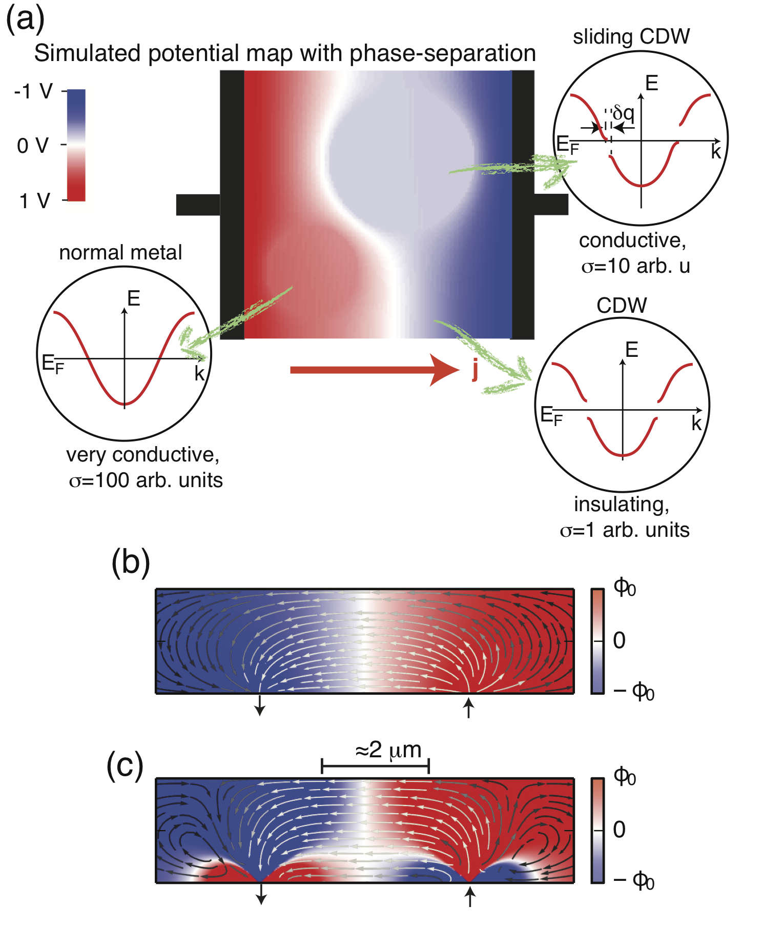
The combination of spectroscopy and local potential mapping could also give access to a number of other phenomena. A particularly interesting example is the recently discovered viscous current flow in graphene Torre et al. 2015; Bandurin et al. 2016; Krishna Kumar et al. 2017; Ella et al. 2019; Sulpizio et al. 2019; Polini and Geim 2020. This unusual hydrodynamic flow regime of the electron liquid can only be reached when the electron-electron scattering length becomes significantly shorter than the sample dimensions and the electron-phonon and electron-defect scattering length Torre et al. 2015. In this regime, which has otherwise only been realised in (Al,Ga)As heterostructures de Jong and Molenkamp 1995, phenomena such as electron “whirlpools” appear in potential maps calculated from the hydrodynamic transport equations. Examples of potential maps with and without viscosity are given in Figure 18(b) and (c), respectively (from Ref. Torre et al. 2015). In transport experiments Bandurin et al. 2016, the existence of current vortices and electron “back-flow” can only be inferred indirectly from voltage measurements at the side contacts of a device, even though it has recently become possible to image such situations directly by scanning-sensor techniques Ella et al. 2019; Sulpizio et al. 2019. In operando nanoARPES could complement these techniques by simultaneously probing the local spectral function and the potential in the device.
Local potential mapping can also be used to disentangle bulk and surface contributions to transport, an aspect which is particularly relevant to topological insulator research. Topological insulators are expected to be bulk insulators or semiconductors supporting metallic surface states Hasan and Kane 2010; Ando 2013. At sufficiently low temperature, the bulk carriers are frozen out and the surface states should thus give rise to a 2D conductance. Unfortunately, this is rarely the case. In fact, topological insulators are plagued by bulk-dominated conductance due to unintended doping and / or small band gaps. In a given transport situation, it is not trivial to determine if the conductance is through surface or bulk states even though 2D vs. 3D transport can be distinguished by collinear four point probes with variable spacing (or movable contacts) Barreto et al. 2014, due to the different functional form of the potential decay in a 2D plane and on the surface of a semi-infinite bulk ( vs ) Hofmann and Wells 2009; Perkins et al. 2013. Mapping the potential in nanoARPES can directly yield this functional form and help to disentangle surface and bulk contributions to transport. This is illustrated in Figure 9 where not only the penetration of the current into the bulk is different but also the distribution along the surface. Even when the detected transport regime is found to be 2D rather than 3D in a transport measurement, it cannot be concluded that it is only the topological surface state that gives rise to metallic transport since several topological insulator materials support band bending-induced (and topologically trivial) two-dimensional metallic states at the surface Bianchi et al. 2010; Benia et al. 2011; King et al. 2011. The simultaneous mapping of the spectral function by nanoARPES, however, would ensure that all contributions to metallic transport can be identified.
Some of the above effects are quite subtle and put high demands on the local potential mapping. In the proof-of-principle from Ref. Curcio et al. 2020 illustrated in Figure 16, the local potential mapping was carried out by fitting a 2D model spectral function to the data. The model is constructed from a Dirac-cone dispersion with the possibility of shifts in energy and , as well as broadening, combined with a Fermi-Dirac distribution. The local Fermi energy from the fit is then used as a map of the potential. This is not a particularly good way of obtaining a potential map because, in the case of almost un-doped graphene, only a vanishingly small spectral feature is present at , resulting in a low accuracy of the value obtained from a fit. A far better approach to measuring such maps would be to use a sharp core level and map the core level binding energy across the sample. This would greatly increase both accuracy and precision. Note that when fitting core level peaks, the resulting uncertainty of the energy position can be very small, in the order of 1 meV, even if the peaks are broad (in the order of 100 meV).
VIII Conclusions
The combination of recent advances in nanoARPES, 2D materials and device fabrication is now permitting in operando studies of field effect transistor-like devices made of 2D QMs, such as graphene or few layer TMDCs. We have discussed the first experimental demonstrations of tracking a material’s doping, spectral function and many body-effects upon gating and while passing a current through the material. While this technique is still in its infancy, it provides a unique new insight into the properties of operating devices and it should be possible to extend the approach to a wide range of QMs showing electric field and current-induced phenomena, such as doping-induced transitions to superconducting or correlated states, field-induced insulator-to-metal transitions in Mott insulators or the field-induced sliding of charge density waves. A side product of mapping the spectral function of a current-carrying device is a position-resolved map of the potential. This can be used to combine spectroscopic and contact-free transport measurements on the nano-scale, determining properties such as the local conductivity or carrier mobility.
IX acknowledgement
The author acknowledges inspiring discussions with Søren Ulstrup, Jill A. Miwa, Marco Bianchi, Jyoti Katoch, Alfred J. H. Jones, Davide Curcio, Deepnarayan Biswas, Paulina Majchrzak, Charlotte E. Sanders, Klara Volckaert, Eli Rotenberg, Aaron Bostwick, Cephise Cacho, Pavel Dudin, Kai Rossnagel and Frederick Joucken. I especially thank SU, AJHJ, JAM, DC, KR and PD for critical comments on the manuscript. This work was supported by VILLUM FONDEN via the Centre of Excellence for Dirac Materials (Grant No. 11744).
This paper is dedicated to the memory of E. Ward Plummer (30.10.1940 - 23.7.2020).
X data availability
The data that support the findings of this study are available from the corresponding author upon reasonable request.
References
- Plummer and Eberhardt (1982) E. W. Plummer and W. Eberhardt, Advances in Chemical Physics 49, 533 (1982).
- Kevan (1992) S. D. Kevan, ed., Angle-resolved photoemission, vol. 74 of Studies in Surface Chemistry and Catalysis (Elsevier, Amsterdam, 1992).
- Hüfner (2003) S. Hüfner, Photoelectron spectroscopy (Springer, Berlin, 2003), 3rd ed.
- Damascelli et al. (2003) A. Damascelli, Z. Hussain, and Z.-X. Shen, Reviews of Modern Physics 75, 473 (2003).
- Hofmann et al. (2009) P. Hofmann, I. Y. Sklyadneva, E. D. L. Rienks, and E. V. Chulkov, New Journal of Physics 11, 125005 (2009).
- Lu et al. (2012) D. Lu, I. M. Vishik, M. Yi, Y. Chen, R. G. Moore, and Z.-X. Shen, Annual Review of Condensed Matter Physics 3, 129 (2012).
- Sobota et al. (2020) J. A. Sobota, Y. He, and Z.-X. Shen (2020), eprint arXiv.2008.02378.
- Rotenberg (2010) E. Rotenberg, in Many-Body Interactions in Nanoscale Materials by Angle-Resolved Photoemission Spectroscopy, edited by J. a. Guo (Wiley-VCH, 2010), p. 169.
- Keimer et al. (2015) B. Keimer, S. A. Kivelson, M. R. Norman, S. Uchida, and J. Zaanen, Nature 518, 179 (2015).
- Keimer and Moore (2017) B. Keimer and J. E. Moore, Nature Physics 13, 1045 (2017).
- Basov et al. (2017) D. N. Basov, R. D. Averitt, and D. Hsieh, Nature Materials 16, 1077 (2017).
- Tokura et al. (2017) Y. Tokura, M. Kawasaki, and N. Nagaosa, Nature Physics 13, 1056 (2017).
- Vojta (2003) M. Vojta, Reports on Progress in Physics 66, 2069 (2003).
- Wang et al. (2013) Y. H. Wang, H. Steinberg, P. Jarillo-Herrero, and N. Gedik, Science 342, 453 (2013).
- Rudner and Lindner (2020) M. S. Rudner and N. H. Lindner, Nature Reviews Physics 2, 229 (2020).
- Cavalleri et al. (2001) A. Cavalleri, C. Tóth, C. W. Siders, J. A. Squier, F. Ráksi, P. Forget, and J. C. Kieffer, Physical Review Letters 87 (2001).
- Schmitt et al. (2008) F. Schmitt, P. S. Kirchmann, U. Bovensiepen, R. G. Moore, L. Rettig, M. Krenz, J. H. Chu, N. Ru, L. Perfetti, D. H. Lu, et al., Science 321, 1649 (2008).
- Rohwer et al. (2011) T. Rohwer, S. Hellmann, M. Wiesenmayer, C. Sohrt, A. Stange, B. Slomski, A. Carr, Y. Liu, L. M. Avila, M. Kallane, et al., Nature 471, 490 (2011).
- Fausti et al. (2011) D. Fausti, R. I. Tobey, N. Dean, S. Kaiser, A. Dienst, M. C. Hoffmann, S. Pyon, T. Takayama, H. Takagi, and A. Cavalleri, Science 331, 189 (2011).
- Mitrano et al. (2016) M. Mitrano, A. Cantaluppi, D. Nicoletti, S. Kaiser, A. Perucchi, S. Lupi, P. Di Pietro, D. Pontiroli, M. Riccò, S. R. Clark, et al., Nature 530, 461 (2016).
- Caputo et al. (2018) M. Caputo, L. Khalil, E. Papalazarou, N. Nilforoushan, L. Perfetti, A. Taleb-Ibrahimi, Q. D. Gibson, R. J. Cava, and M. Marsi, Physical Review B 97 (2018).
- Taguchi et al. (2000) Y. Taguchi, T. Matsumoto, and Y. Tokura, Phys. Rev. B 62, 7015 (2000).
- Lee et al. (2007) S. Lee, A. Fursina, J. T. Mayo, C. T. Yavuz, V. L. Colvin, R. G. Sumesh Sofin, I. V. Shvets, and D. Natelson, Nature Materials 7, 130 (2007).
- Vaju et al. (2008) C. Vaju, L. Cario, B. Corraze, E. Janod, V. Dubost, T. Cren, D. Roditchev, D. Braithwaite, and O. Chauvet, Advanced Materials 20, 2760 (2008).
- Monceau (2012) P. Monceau, Advances in Physics 61, 325 (2012).
- Stoliar et al. (2013) P. Stoliar, L. Cario, E. Janod, B. Corraze, C. Guillot-Deudon, S. Salmon-Bourmand, V. Guiot, J. Tranchant, and M. Rozenberg, Advanced Materials 25, 3222 (2013).
- Nakamura et al. (2013) F. Nakamura, M. Sakaki, Y. Yamanaka, S. Tamaru, T. Suzuki, and Y. Maeno, Scientific Reports 3, 2536 (2013).
- Bellec et al. (2020) E. Bellec, I. Gonzalez-Vallejo, V. L. R. Jacques, A. A. Sinchenko, A. P. Orlov, P. Monceau, S. J. Leake, and D. Le Bolloc’h, Phys. Rev. B 101, 125122 (2020).
- Bertinshaw et al. (2019) J. Bertinshaw, N. Gurung, P. Jorba, H. Liu, M. Schmid, D. T. Mantadakis, M. Daghofer, M. Krautloher, A. Jain, G. H. Ryu, et al., Physical Review Letters 123 (2019).
- Cirillo et al. (2019) C. Cirillo, V. Granata, G. Avallone, R. Fittipaldi, C. Attanasio, A. Avella, and A. Vecchione, Physical Review B 100 (2019).
- Zhang et al. (2019) J. Zhang, A. S. McLeod, Q. Han, X. Chen, H. A. Bechtel, Z. Yao, S. N. Gilbert Corder, T. Ciavatti, T. H. Tao, M. Aronson, et al., Physical Review X 9 (2019).
- Mattoni et al. (2020) G. Mattoni, S. Yonezawa, F. Nakamura, and Y. Maeno, arXiv (2020), eprint arXiv.2007.06885.
- Nakatsuji and Maeno (2000) S. Nakatsuji and Y. Maeno, Phys. Rev. Lett. 84, 2666 (2000).
- Nakamura et al. (2002) F. Nakamura, T. Goko, M. Ito, T. Fujita, S. Nakatsuji, H. Fukazawa, Y. Maeno, P. Alireza, D. Forsythe, and S. R. Julian, Phys. Rev. B 65, 220402 (2002).
- Riccò et al. (2018) S. Riccò, M. Kim, A. Tamai, S. McKeown Walker, F. Y. Bruno, I. Cucchi, E. Cappelli, C. Besnard, T. K. Kim, P. Dudin, et al., Nature Communications 9, 4535 (2018).
- Sunko et al. (2019) V. Sunko, E. A. Morales, I. Marković, M. E. Barber, D. Milosavljević, F. Mazzola, D. A. Sokolov, N. Kikugawa, C. Cacho, P. Dudin, et al., npj Quantum Materials 4 (2019).
- Ashcroft and Mermin (1976) N. E. Ashcroft and N. D. Mermin, Solid state physics (Saunders College, Philadelphia, 1976), international ed.
- Flötotto et al. (2018) D. Flötotto, Y. Bai, Y.-H. Chan, P. Chen, X. Wang, P. Rossi, C.-Z. Xu, C. Zhang, J. A. Hlevyack, J. D. Denlinger, et al., Nano Letters 18, 5628 (2018).
- Lin et al. (2020) C. Lin, M. Ochi, R. Noguchi, K. Kuroda, M. Sakoda, A. Nomura, M. Tsubota, P. Zhang, C. Bareille, K. Kurokawa, et al. (2020), eprint arXiv.2009.06353.
- Noguchi et al. (2019) R. Noguchi, T. Takahashi, K. Kuroda, M. Ochi, T. Shirasawa, M. Sakano, C. Bareille, M. Nakayama, M. D. Watson, K. Yaji, et al., Nature 566, 518 (2019).
- Kastl et al. (2019) C. Kastl, R. J. Koch, C. T. Chen, J. Eichhorn, S. Ulstrup, A. Bostwick, C. Jozwiak, T. R. Kuykendall, N. J. Borys, F. M. Toma, et al., ACS Nano 13, 1284 (2019).
- Ulstrup et al. (2019a) S. Ulstrup, C. E. Giusca, J. A. Miwa, C. E. Sanders, A. Browning, P. Dudin, C. Cacho, O. Kazakova, D. K. Gaskill, R. L. Myers-Ward, et al., Nature Communications 10, 3283 (2019a).
- Utama et al. (2020) M. I. B. Utama, R. J. Koch, K. Lee, N. Leconte, H. Li, S. Zhao, L. Jiang, J. Zhu, K. Watanabe, T. Taniguchi, et al., Nature Physics (2020).
- Lisi et al. (2020) S. Lisi, X. Lu, T. Benschop, T. A. de Jong, P. Stepanov, J. R. Duran, F. Margot, I. Cucchi, E. Cappelli, A. Hunter, et al., Nature Physics (2020).
- Ulstrup et al. (2020) S. Ulstrup, R. J. Koch, S. Singh, K. M. McCreary, B. T. Jonker, J. T. Robinson, C. Jozwiak, E. Rotenberg, A. Bostwick, J. Katoch, et al., Science Advances 6, eaay6104 (2020).
- Klitzing et al. (1980) K. v. Klitzing, G. Dorda, and M. Pepper, Phys. Rev. Lett. 45, 494 (1980).
- Tsui et al. (1982) D. C. Tsui, H. L. Stormer, and A. C. Gossard, Phys. Rev. Lett. 48, 1559 (1982).
- Konig et al. (2007) M. Konig, S. Wiedmann, C. Brune, A. Roth, H. Buhmann, L. W. Molenkamp, X.-L. Qi, and S.-C. Zhang, Science 318, 766 (2007).
- Bednorz and Müller (1986) J. G. Bednorz and K. A. Müller, Zeitschrift für Physik B Condensed Matter 64, 189 (1986).
- Grüner (1994) G. Grüner, Density waves in solids, vol. 89 of Frontiers in physics (Perseus Publishing, Cambridge, Massachusetts, 1994).
- King et al. (2010) P. D. C. King, T. D. Veal, C. F. McConville, J. Zúñiga Pérez, V. Muñoz Sanjosé, M. Hopkinson, E. D. L. Rienks, M. F. Jensen, and P. Hofmann, Phys. Rev. Lett. 104, 256803 (2010).
- Bianchi et al. (2010) M. Bianchi, D. Guan, S. Bao, J. Mi, B. B. Iversen, P. D. C. King, and P. Hofmann, Nature Communications 1, 128 (2010).
- Santander-Syro et al. (2011) A. F. Santander-Syro, O. Copie, T. Kondo, F. Fortuna, S. Pailhès, R. Weht, X. G. Qiu, F. Bertran, A. Nicolaou, A. Taleb-Ibrahimi, et al., Nature 469, 189 (2011).
- Meevasana et al. (2011) W. Meevasana, P. D. C. King, R. H. He, S.-K. Mo, M. Hashimoto, A. Tamai, P. Songsiriritthigul, F. Baumberger, and Z.-X. Shen, Nature Materials 10, 114 (2011).
- Kim et al. (2015) J. Kim, S. S. Baik, S. H. Ryu, Y. Sohn, S. Park, B.-G. Park, J. Denlinger, Y. Yi, H. J. Choi, and K. S. Kim, Science 349, 723 (2015).
- Novoselov et al. (2005) K. S. Novoselov, D. Jiang, F. Schedin, T. J. Booth, V. V. Khotkevich, S. V. Morozov, and A. K. Geim, Proceedings of the National Academy of Sciences of the United States of America 102, 10451 (2005).
- Novoselov et al. (2004) K. S. Novoselov, A. K. Geim, S. V. Morozov, D. Jiang, Y. Zhang, S. V. Dubonos, I. V. Grigorieva, and A. A. Firsov, Science 306, 666 (2004).
- Zhang et al. (2005) Y. B. Zhang, Y. W. Tan, H. L. Stormer, and P. Kim, Nature 438, 201 (2005).
- Neto et al. (2009) A. H. C. Neto, F. Guinea, N. M. R. Peres, K. S. Novoselov, and A. K. Geim, Reviews of Modern Physics 81, 109 (2009).
- Kara et al. (2012) A. Kara, H. Enriquez, A. P. Seitsonen, L. Lew Yan Voon, S. Vizzini, B. Aufray, and H. Oughaddou, Surface Science Reports 67, 1 (2012).
- Basov et al. (2014) D. N. Basov, M. M. Fogler, A. Lanzara, F. Wang, and Y. Zhang, Rev. Mod. Phys. 86, 959 (2014).
- Das et al. (2015) S. Das, J. A. Robinson, M. Dubey, H. Terrones, and M. Terrones, Annual Review of Materials Research 45, 1 (2015).
- Avouris et al. (2017) P. Avouris, T. F. Heinz, and T. Low, eds., 2D Materials: Properties and Devices (Cambridge University Press, 2017).
- Manzeli et al. (2017) S. Manzeli, D. Ovchinnikov, D. Pasquier, O. V. Yazyev, and A. Kis, Nature Reviews Materials 2, 17033 (2017).
- Dong and Kuljanishvili (2017) R. Dong and I. Kuljanishvili, Journal of Vacuum Science and Technology B, Nanotechnology and Microelectronics: Materials, Processing, Measurement, and Phenomena 35, 030803 (2017).
- Zhao and Jia (2020) C.-X. Zhao and J.-F. Jia, Frontiers of Physics 15 (2020).
- Andrei and MacDonald (2020) E. Y. Andrei and A. H. MacDonald (2020), eprint arXiv.2008.08129.
- Arnold et al. (2018) F. Arnold, R.-M. Stan, S. K. Mahatha, H. E. Lund, D. Curcio, M. Dendzik, H. Bana, E. Travaglia, L. Bignardi, P. Lacovig, et al., 2D Materials 5, 045009 (2018).
- Radisavljevic et al. (2011) B. Radisavljevic, A. Radenovic, J. Brivio, V. Giacometti, and A. Kis, Nature Nanotechnology 6, 147 (2011).
- Costanzo et al. (2016) D. Costanzo, S. Jo, H. Berger, and A. F. Morpurgo, Nat Nano 11, 339 (2016).
- Radisavljevic and Kis (2013) B. Radisavljevic and A. Kis, Nature Materials 12, 815 (2013).
- Dean et al. (2010) C. R. Dean, A. F. Young, I. Meric, C. Lee, L. Wang, S. Sorgenfrei, K. Watanabe, T. Taniguchi, P. Kim, K. L. Shepard, et al., Nature Nanotechnology 5, 722 (2010).
- Watanabe et al. (2004) K. Watanabe, T. Taniguchi, and H. Kanda, Nature Materials 3, 404 (2004).
- Geim and Grigorieva (2013) A. K. Geim and I. V. Grigorieva, Nature 499, 419 (2013).
- Novoselov et al. (2016) K. S. Novoselov, A. Mishchenko, A. Carvalho, and A. H. C. Neto, Science 353, aac9439 (2016).
- Cheng et al. (2014) R. Cheng, D. Li, H. Zhou, C. Wang, A. Yin, S. Jiang, Y. Liu, Y. Chen, Y. Huang, and X. Duan, Nano Letters 14, 5590 (2014).
- Wilson et al. (2017) N. R. Wilson, P. V. Nguyen, K. Seyler, P. Rivera, A. J. Marsden, Z. P. L. Laker, G. C. Constantinescu, V. Kandyba, A. Barinov, N. D. M. Hine, et al., Science Advances 3 (2017).
- Zribi et al. (2019) J. Zribi, L. Khalil, B. Zheng, J. Avila, D. Pierucci, T. Brulé, J. Chaste, E. Lhuillier, M. C. Asensio, A. Pan, et al., npj 2D Materials and Applications 3 (2019).
- Avsar et al. (2014) A. Avsar, J. Y. Tan, T. Taychatanapat, J. Balakrishnan, G. K. W. Koon, Y. Yeo, J. Lahiri, A. Carvalho, A. S. Rodin, E. C. T. O’Farrell, et al., Nature Communications 5, 4875 (2014).
- Li et al. (2020) L. Li, S. Jiang, Z. Wang, K. Watanabe, T. Taniguchi, J. Shan, and K. F. Mak, Phys. Rev. Materials 4, 104005 (2020).
- Lüpke et al. (2020) F. Lüpke, D. Waters, S. C. de la Barrera, M. Widom, D. G. Mandrus, J. Yan, R. M. Feenstra, and B. M. Hunt, Nature Physics 16, 526 (2020).
- Žutić et al. (2019) I. Žutić, A. Matos-Abiague, B. Scharf, H. Dery, and K. Belashchenko, Materials Today 22, 85 (2019).
- Cao et al. (2018a) Y. Cao, V. Fatemi, A. Demir, S. Fang, S. L. Tomarken, J. Y. Luo, J. D. Sanchez-Yamagishi, K. Watanabe, T. Taniguchi, E. Kaxiras, et al., Nature 556, 80 (2018a).
- Cao et al. (2018b) Y. Cao, V. Fatemi, S. Fang, K. Watanabe, T. Taniguchi, E. Kaxiras, and P. Jarillo-Herrero, Nature 556, 43 (2018b).
- Frisenda et al. (2018) R. Frisenda, E. Navarro-Moratalla, P. Gant, D. Pérez De Lara, P. Jarillo-Herrero, R. V. Gorbachev, and A. Castellanos-Gomez, Chem. Soc. Rev. 47, 53 (2018).
- Haastrup et al. (2018) S. Haastrup, M. Strange, M. Pandey, T. Deilmann, P. S. Schmidt, N. F. Hinsche, M. N. Gjerding, D. Torelli, P. M. Larsen, A. C. Riis-Jensen, et al., 2D Materials 5, 042002 (2018).
- Hou et al. (2020) Y. Hou, T. Zhang, J. Sun, L. Liu, Y. Yao, and Y. Wang (2020), eprint arXiv.2008.04150.
- Reis et al. (2017) F. Reis, G. Li, L. Dudy, M. Bauernfeind, S. Glass, W. Hanke, R. Thomale, J. Schäfer, and R. Claessen, Science 357, 287 (2017).
- Jensen and Plummer (1985) E. Jensen and E. W. Plummer, Physical Review Letters 55, 1912 (1985).
- Mårtensson et al. (1994) N. Mårtensson, P. Baltzer, P. Brühwiler, J.-O. Forsell, A. Nilsson, A. Stenborg, and B. Wannberg, Journal of Electron Spectroscopy and Related Phenomena 70, 117 (1994).
- Lanzara et al. (2001) A. Lanzara, P. V. Bogdanov, X. J. Zhou, S. A. Kellar, D. L. Feng, E. D. Lu, T. Yoshida, H. Eisaki, A. Fujimori, K. Kishio, et al., Nature 412, 510 (2001).
- Kiss et al. (2008) T. Kiss, T. Shimojima, K. Ishizaka, A. Chainani, T. Togashi, T. Kanai, X.-Y. Wang, C.-T. Chen, S. Watanabe, and S. Shin, Review of Scientific Instruments 79, 023106 (2008).
- Borisenko (2012) S. V. Borisenko, Synchrotron Radiation News 25, 6 (2012).
- Suga and Tusche (2015) S. Suga and C. Tusche, Journal of Electron Spectroscopy and Related Phenomena 200, 119 (2015).
- Strocov et al. (2019) V. N. Strocov, L. L. Lev, M. Kobayashi, C. Cancellieri, M. A. Husanu, A. Chikina, N. B. M. Schröter, X. Wang, J. A. Krieger, and Z. Salman, k-resolved electronic structure of buried heterostructure and impurity systems by soft-x-ray arpes (2019), eprint arXiv.1906.11025.
- Miwa et al. (2015) J. A. Miwa, S. Ulstrup, S. G. Sørensen, M. Dendzik, A. G. Čabo, M. Bianchi, J. V. Lauritsen, and P. Hofmann, Phys. Rev. Lett. 114, 046802 (2015).
- Penn (1976) D. R. Penn, Physical Review B 13, 5248 (1976).
- Zangwill (1988) A. Zangwill, Physics at Surfaces (and references therein). (Cambridge University Press, 1988).
- Hengsberger et al. (1999) M. Hengsberger, D. Purdie, P. Segovia, M. Garnier, and Y. Baer, Physical Review Letters 83, 592 (1999).
- Valla et al. (1999a) T. Valla, A. V. Fedorov, P. D. Johnson, and S. L. Hulbert, Physical Review Letters 83, 2085 (1999a).
- Valla et al. (1999b) T. Valla, A. V. Fedorov, P. D. Johnson, B. O. Wells, S. L. Hulbert, Q. Li, G. D. Gu, and N. Koshizuka, Science 285, 2110 (1999b).
- Engelsberg and Schrieffer (1963) S. Engelsberg and J. R. Schrieffer, Physical Review 131, 993 (1963).
- Kordyuk et al. (2005) A. A. Kordyuk, S. V. Borisenko, A. Koitzsch, J. Fink, M. Knupfer, and H. Berger, Physical Review B 71, 214513 (2005).
- Pletikosić et al. (2012) I. Pletikosić, M. Kralj, M. Milun, and P. Pervan, Phys. Rev. B 85, 155447 (2012).
- Luttinger and Ward (1960) J. M. Luttinger and J. C. Ward, Phys. Rev. 118, 1417 (1960).
- Nechaev et al. (2009) I. A. Nechaev, M. F. Jensen, E. D. L. Rienks, V. M. Silkin, P. M. Echenique, E. V. Chulkov, and P. Hofmann, Physical Review B 80, 113402 (2009).
- Mazzola et al. (2013) F. Mazzola, J. W. Wells, R. Yakimova, S. Ulstrup, J. A. Miwa, R. Balog, M. Bianchi, M. Leandersson, J. Adell, P. Hofmann, et al., Phys. Rev. Lett. 111, 216806 (2013).
- Karolak et al. (2011) M. Karolak, T. O. Wehling, F. Lechermann, and A. I. Lichtenstein, Journal of Physics: Condensed Matter 23, 085601 (2011).
- Usachov et al. (2011) D. Usachov, O. Vilkov, A. Grüneis, D. Haberer, A. Fedorov, V. K. Adamchuk, A. B. Preobrajenski, P. Dudin, A. Barinov, M. Oehzelt, et al., Nano Letters 11, 5401 (2011).
- Henck et al. (2018) H. Henck, J. Avila, Z. Ben Aziza, D. Pierucci, J. Baima, B. Pamuk, J. Chaste, D. Utt, M. Bartos, K. Nogajewski, et al., Phys. Rev. B 97, 245421 (2018).
- Kastl et al. (2018) C. Kastl, C. T. Chen, R. J. Koch, B. Schuler, T. R. Kuykendall, A. Bostwick, C. Jozwiak, T. Seyller, E. Rotenberg, A. Weber-Bargioni, et al., 2D Materials 5, 045010 (2018).
- Teo et al. (2008) J. C. Y. Teo, L. Fu, and C. L. Kane, Physical Review B 78, 045426 (2008).
- Wu et al. (2020) X. Wu, J. Li, X.-M. Ma, Y. Zhang, Y. Liu, C.-S. Zhou, J. Shao, Q. Wang, Y.-J. Hao, Y. Feng, et al., Physical Review X 10 (2020).
- Zhu and Hofmann (2014) X.-G. Zhu and P. Hofmann, Phys. Rev. B 89, 125402 (2014).
- Takeuchi et al. (1991) N. Takeuchi, C. T. Chan, and K. M. Ho, Phys. Rev. B 43, 13899 (1991).
- Zhang et al. (2011) P. Zhang, P. Richard, T. Qian, Y.-M. Xu, X. Dai, and H. Ding, Review of Scientific Instruments 82, 043712 (2011).
- Zhang et al. (2009) Y. Zhang, V. W. Brar, C. Girit, A. Zettl, and M. F. Crommie, Nature Physics 5, 722 (2009).
- Beidenkopf et al. (2011) H. Beidenkopf, P. Roushan, J. Seo, L. Gorman, I. Drozdov, Y. S. Hor, R. J. Cava, and A. Yazdani, Nature Physics 7, 939 (2011).
- Fujikawa et al. (2009) Y. Fujikawa, T. Sakurai, and R. M. Tromp, Physical Review B 79 (2009).
- Sutter et al. (2009) P. Sutter, M. S. Hybertsen, J. T. Sadowski, and E. Sutter, Nano Letters 9, 2654 (2009).
- Jin et al. (2013) W. Jin, P.-C. Yeh, N. Zaki, D. Zhang, J. T. Sadowski, A. Al-Mahboob, A. M. van der Zande, D. A. Chenet, J. I. Dadap, I. P. Herman, et al., Phys. Rev. Lett. 111, 106801 (2013).
- Cattelan and Fox (2018) M. Cattelan and N. Fox, Nanomaterials 8, 284 (2018).
- Ulstrup et al. (2019b) S. Ulstrup, R. J. Koch, D. Schwarz, K. M. McCreary, B. T. Jonker, S. Singh, A. Bostwick, E. Rotenberg, C. Jozwiak, and J. Katoch, Applied Physics Letters 114, 151601 (2019b).
- Escher et al. (2005) M. Escher, N. Weber, M. Merkel, C. Ziethen, P. Bernhard, G. Schönhense, S. Schmidt, F. Forster, F. Reinert, B. Krömker, et al., Journal of Physics: Condensed Matter 17, S1329 (2005).
- Krömker et al. (2008) B. Krömker, M. Escher, D. Funnemann, D. Hartung, H. Engelhard, and J. Kirschner, Review of Scientific Instruments 79, 053702 (2008).
- Wiemann et al. (2011) C. Wiemann, M. Patt, I. P. Krug, N. B. Weber, M. Escher, M. Merkel, and C. M. Schneider, e-Journal of Surface Science and Nanotechnology 9, 395 (2011).
- Schönhense et al. (2015) G. Schönhense, K. Medjanik, and H.-J. Elmers, Journal of Electron Spectroscopy and Related Phenomena 200, 94 (2015).
- Tusche et al. (2019) C. Tusche, Y.-J. Chen, C. M. Schneider, and J. Kirschner, Ultramicroscopy 206, 112815 (2019).
- Matsui et al. (2020) F. Matsui, S. Makita, H. Matsuda, T. Yano, E. Nakamura, K. Tanaka, S. Suga, and S. Kera, Japanese Journal of Applied Physics 59, 067001 (2020).
- Rotenberg and Bostwick (2014) E. Rotenberg and A. Bostwick, Journal of Synchrotron Radiation 21, 1048 (2014).
- Avila et al. (2013) J. Avila, I. Razado-Colambo, S. Lorcy, B. Lagarde, J.-L. Giorgetta, F. Polack, and M. C. Asensio, Journal of Physics: Conference Series 425, 192023 (2013).
- Avila and Asensio (2014) J. Avila and M. C. Asensio, Synchrotron Radiation News 27, 24 (2014).
- Rösner et al. (2019) B. Rösner, P. Dudin, J. Bosgra, M. Hoesch, and C. David, Journal of Synchrotron Radiation 26, 467 (2019).
- Dudin et al. (2010) P. Dudin, P. Lacovig, C. Fava, E. Nicolini, A. Bianco, G. Cautero, and A. Barinov, Journal of Synchrotron Radiation 17, 445 (2010).
- Nguyen et al. (2019) P. V. Nguyen, N. C. Teutsch, N. P. Wilson, J. Kahn, X. Xia, A. J. Graham, V. Kandyba, A. Giampietri, A. Barinov, G. C. Constantinescu, et al., Nature 572, 220 (2019).
- Koch et al. (2018) R. J. Koch, C. Jozwiak, A. Bostwick, B. Stripe, M. Cordier, Z. Hussain, W. Yun, and E. Rotenberg, Synchrotron Radiation News 31, 50 (2018).
- Curcio et al. (2020) D. Curcio, A. J. H. Jones, R. Muzzio, K. Volckaert, D. Biswas, C. E. Sanders, P. Dudin, C. Cacho, S. Singh, K. Watanabe, et al., Phys. Rev. Lett. 125, 236403 (2020).
- Liu et al. (2019) Y. Liu, S. Zhang, J. He, Z. M. Wang, and Z. Liu, Nano-Micro Letters 11 (2019).
- Fan et al. (2020) S. Fan, Q. A. Vu, M. D. Tran, S. Adhikari, and Y. H. Lee, 2D Materials 7, 022005 (2020).
- Ju et al. (2014) L. Ju, J. Velasco, E. Huang, S. Kahn, C. Nosiglia, H.-Z. Tsai, W. Yang, T. Taniguchi, K. Watanabe, Y. Zhang, et al., Nature Nanotechnology 9, 348 (2014).
- Zhang et al. (2013) T. Zhang, N. Levy, J. Ha, Y. Kuk, and J. A. Stroscio, Phys. Rev. B 87, 115410 (2013).
- Kevan (1986) S. Kevan, Physical Review B 33, 4364 (1986).
- Kretinin et al. (2014) A. V. Kretinin, Y. Cao, J. S. Tu, G. L. Yu, R. Jalil, K. S. Novoselov, S. J. Haigh, A. Gholinia, A. Mishchenko, M. Lozada, et al., Nano Letters 14, 3270 (2014).
- Muzzio et al. (2020) R. Muzzio, A. J. H. Jones, D. Curcio, D. Biswas, J. A. Miwa, P. Hofmann, K. Watanabe, T. Taniguchi, S. Singh, C. Jozwiak, et al., Physical Review B 101, 201409 (2020).
- Kaminski et al. (2016) A. Kaminski, S. Rosenkranz, M. R. Norman, M. Randeria, Z. Z. Li, H. Raffy, and J. C. Campuzano, Phys. Rev. X 6, 031040 (2016).
- Naamneh et al. (2016) M. Naamneh, J. C. Campuzano, and A. Kanigel (2016), eprint arXiv.1607.02901.
- (147) By the surface conductance being 20 times higher than the bulk conductance, we do not refer to a 2D surface conductance compared to a 3D bulk conductance. We merely mean that the top layer voxels in the simulation have a conductivity that is 20 times higher than that of all the other voxels. The depth of the first layer voxels is 60 times smaller than the distance between the contacts.
- Wells et al. (2006) J. W. Wells, J. F. Kallehauge, T. M. Hansen, and P. Hofmann, Physical Review Letters 97, 206803 (2006).
- Hofmann and Wells (2009) P. Hofmann and J. W. Wells, Journal of Physics: Condensed Matter 21, 013003 (2009).
- Perkins et al. (2013) E. Perkins, L. Barreto, J. Wells, and P. Hofmann, Review of Scientific Instruments 84, 033901 (2013).
- Barreto et al. (2014) L. Barreto, L. Kühnemund, F. Edler, C. Tegenkamp, J. Mi, M. Bremholm, B. B. Iversen, C. Frydendahl, M. Bianchi, and P. Hofmann, Nano Letters 14, 3755 (2014).
- Joucken et al. (2016) F. Joucken, N. Reckinger, S. Lorcy, J. Avila, C. Chen, J. Lagoute, J.-F. m. c. Colomer, J. Ghijsen, M. C. Asensio, and R. Sporken, Phys. Rev. B 93, 241101 (2016).
- Joucken et al. (2019a) F. Joucken, E. A. Quezada-López, J. Avila, C. Chen, J. L. Davenport, H. Chen, K. Watanabe, T. Taniguchi, M. C. Asensio, and J. Velasco, Phys. Rev. B 99, 161406 (2019a).
- Paradisi et al. (2015) A. Paradisi, J. Biscaras, and A. Shukla, Applied Physics Letters 107, 143103 (2015).
- Rosenzweig et al. (2020) P. Rosenzweig, H. Karakachian, D. Marchenko, K. Küster, and U. Starke, Phys. Rev. Lett. 125, 176403 (2020).
- Zhang et al. (2008) Y. Zhang, V. W. Brar, F. Wang, C. Girit, Y. Yayon, M. Panlasigui, A. Zettl, and M. F. Crommie, Nature Physics 4, 627 (2008).
- Joucken et al. (2019b) F. Joucken, J. Avila, Z. Ge, E. A. Quezada-Lopez, H. Yi, R. Le Goff, E. Baudin, J. L. Davenport, K. Watanabe, T. Taniguchi, et al., Nano Letters 19, 2682 (2019b).
- McCann (2006) E. McCann, Phys. Rev. B 74, 161403 (2006).
- Ohta et al. (2006) T. Ohta, A. Bostwick, T. Seyller, K. Horn, and E. Rotenberg, Science 313, 951 (2006).
- Kipp et al. (1999) L. Kipp, K. Roßnagel, C. Solterbeck, T. Strasser, W. Schattke, and M. Skibowski, Physical Review Letters 83, 5551 (1999).
- Gaylord et al. (1989) R. H. Gaylord, K. H. Jeong, and S. D. Kevan, Physical Review Letters 62, 2036 (1989).
- Aebi et al. (1994) P. Aebi, J. Osterwalder, R. Fasel, D. Naumović, and L. Schlapbach, Surface Science 307-309, 917 (1994).
- Shirley et al. (1995) E. L. Shirley, L. J. Terminello, A. Santoni, and F. J. Himpsel, Phys. Rev. B 51, 13614 (1995).
- Mucha-Kruczynski et al. (2008) M. Mucha-Kruczynski, O. Tsyplyatyev, A. Grishin, E. McCann, V. I. Fal’ko, A. Bostwick, and E. Rotenberg, Physical Review B 77, 195403 (2008).
- Lizzit et al. (2010) S. Lizzit, G. Zampieri, L. Petaccia, R. Larciprete, P. Lacovig, E. D. L. Rienks, G. Bihlmayer, A. Baraldi, and P. Hofmann, Nature Physics 6, 345 (2010).
- Gierz et al. (2011) I. Gierz, J. Henk, H. Höchst, C. R. Ast, and K. Kern, Phys. Rev. B 83, 121408 (2011).
- Bostwick et al. (2010) A. Bostwick, F. Speck, T. Seyller, K. Horn, M. Polini, R. Asgari, A. H. MacDonald, and E. Rotenberg, Science 328, 999 (2010).
- Walter et al. (2011) A. L. Walter, A. Bostwick, K.-J. Jeon, F. Speck, M. Ostler, T. Seyller, L. Moreschini, Y. J. Chang, M. Polini, R. Asgari, et al., Phys. Rev. B 84, 085410 (2011).
- Das Sarma and Hwang (2013) S. Das Sarma and E. H. Hwang, Phys. Rev. B 87, 045425 (2013).
- Ulstrup et al. (2016a) S. Ulstrup, M. Schüler, M. Bianchi, F. Fromm, C. Raidel, T. Seyller, T. Wehling, and P. Hofmann, Phys. Rev. B 94, 081403 (2016a).
- Jones et al. (2020) A. J. H. Jones, R. Muzzio, P. Majchrzak, S. Pakdel, D. Curcio, K. Volckaert, D. Biswas, J. Gobbo, S. Singh, J. T. Robinson, et al., Advanced Materials 32, 2001656 (2020).
- Luryi (1988) S. Luryi, Applied Physics Letters 52, 501 (1988).
- Cheiwchanchamnangij and Lambrecht (2012) T. Cheiwchanchamnangij and W. R. L. Lambrecht, Phys. Rev. B 85, 205302 (2012).
- Cappelluti et al. (2013) E. Cappelluti, R. Roldán, J. A. Silva-Guillén, P. Ordejón, and F. Guinea, Phys. Rev. B 88, 075409 (2013).
- Riley et al. (2014) J. M. Riley, F. Mazzola, M. Dendzik, M. Michiardi, T. Takayama, L. Bawden, C. Granerod, M. Leandersson, T. Balasubramanian, M. Hoesch, et al., Nat Phys 10, 835 (2014).
- Mak et al. (2010) K. F. Mak, C. Lee, J. Hone, J. Shan, and T. F. Heinz, Phys. Rev. Lett. 105, 136805 (2010).
- Splendiani et al. (2010) A. Splendiani, L. Sun, Y. Zhang, T. Li, J. Kim, C.-Y. Chim, G. Galli, and F. Wang, Nano Letters 10, 1271 (2010).
- Katoch et al. (2018) J. Katoch, S. Ulstrup, R. J. Koch, S. Moser, K. M. McCreary, S. Singh, J. Xu, B. T. Jonker, R. K. Kawakami, A. Bostwick, et al., Nature Physics 14, 355 (2018).
- Qiu et al. (2013) D. Y. Qiu, F. H. da Jornada, and S. G. Louie, Phys. Rev. Lett. 111, 216805 (2013).
- Grubišić Čabo et al. (2015) A. Grubišić Čabo, J. A. Miwa, S. S. Grønborg, J. M. Riley, J. C. Johannsen, C. Cacho, O. Alexander, R. T. Chapman, E. Springate, M. Grioni, et al., Nano Letters 15, 5883 (2015).
- Ulstrup et al. (2016b) S. Ulstrup, A. G. Čabo, J. A. Miwa, J. M. Riley, S. S. Grønborg, J. C. Johannsen, C. Cacho, O. Alexander, R. T. Chapman, E. Springate, et al., ACS Nano 10, 6315 (2016b).
- Bertoni et al. (2016) R. Bertoni, C. W. Nicholson, L. Waldecker, H. Hübener, C. Monney, U. De Giovannini, M. Puppin, M. Hoesch, E. Springate, R. T. Chapman, et al., Phys. Rev. Lett. 117, 277201 (2016).
- Ulstrup et al. (2017) S. Ulstrup, A. G. c. v. a. c. Čabo, D. Biswas, J. M. Riley, M. Dendzik, C. E. Sanders, M. Bianchi, C. Cacho, D. Matselyukh, R. T. Chapman, et al., Phys. Rev. B 95, 041405 (2017).
- Beyer et al. (2019) H. Beyer, G. Rohde, A. Grubišić Čabo, A. Stange, T. Jacobsen, L. Bignardi, D. Lizzit, P. Lacovig, C. Sanders, S. Lizzit, et al., Physical Review Letters 123 (2019).
- Kutnyakhov et al. (2020) D. Kutnyakhov, R. P. Xian, M. Dendzik, M. Heber, F. Pressacco, S. Y. Agustsson, L. Wenthaus, H. Meyer, S. Gieschen, G. Mercurio, et al., Review of Scientific Instruments 91, 013109 (2020).
- Chernikov et al. (2015a) A. Chernikov, C. Ruppert, H. M. Hill, A. F. Rigosi, and T. F. Heinz, Nat Photon 9, 466 (2015a).
- Eickholt et al. (2018) P. Eickholt, C. Sanders, M. Dendzik, L. Bignardi, D. Lizzit, S. Lizzit, A. Bruix, P. Hofmann, and M. Donath, Phys. Rev. Lett. 121, 136402 (2018).
- Zhang et al. (2015) C. Zhang, Y. Chen, A. Johnson, M.-Y. Li, L.-J. Li, P. C. Mende, R. M. Feenstra, and C.-K. Shih, Nano Letters 15, 6494 (2015).
- Bruix et al. (2016) A. Bruix, J. A. Miwa, N. Hauptmann, D. Wegner, S. Ulstrup, S. S. Grønborg, C. E. Sanders, M. Dendzik, A. Grubišić Čabo, M. Bianchi, et al., Phys. Rev. B 93, 165422 (2016).
- Riley et al. (2015) J. M. Riley, W. Meevasana, L. Bawden, M. Asakawa, T. Takayama, T. Eknapakul, T. K. Kim, M. Hoesch, S. K. Mo, H. Takagi, et al., Nat Nano 10, 1043 (2015).
- Chernikov et al. (2015b) A. Chernikov, A. M. van der Zande, H. M. Hill, A. F. Rigosi, A. Velauthapillai, J. Hone, and T. F. Heinz, Physical Review Letters 115 (2015b).
- Young et al. (2012) A. F. Young, C. R. Dean, I. Meric, S. Sorgenfrei, H. Ren, K. Watanabe, T. Taniguchi, J. Hone, K. L. Shepard, and P. Kim, Phys. Rev. B 85, 235458 (2012).
- Bostwick et al. (2009) A. Bostwick, J. L. McChesney, K. V. Emtsev, T. Seyller, K. Horn, S. D. Kevan, and E. Rotenberg, Physical Review Letters 103, 056404 (pages 4) (2009).
- Muralt and Pohl (1986) P. Muralt and D. W. Pohl, Applied Physics Letters 48, 514 (1986).
- Zhang et al. (2016) H. Zhang, X. Li, Y. Chen, C. Durand, A.-P. Li, and X.-G. Zhang, Review of Scientific Instruments 87, 083702 (2016).
- Tetienne et al. (2017) J.-P. Tetienne, N. Dontschuk, D. A. Broadway, A. Stacey, D. A. Simpson, and L. C. L. Hollenberg, Science Advances 3, e1602429 (2017).
- Voigtländer et al. (2018) B. Voigtländer, V. Cherepanov, S. Korte, A. Leis, D. Cuma, S. Just, and F. Lüpke, Review of Scientific Instruments 89, 101101 (2018).
- Ella et al. (2019) L. Ella, A. Rozen, J. Birkbeck, M. Ben-Shalom, D. Perello, J. Zultak, T. Taniguchi, K. Watanabe, A. K. Geim, S. Ilani, et al., Nature Nanotechnology 14, 480 (2019).
- Gudde et al. (2007) J. Gudde, M. Rohleder, T. Meier, S. W. Koch, and U. Hofer, Science 318, 1287 (2007).
- Reimann et al. (2018) J. Reimann, S. Schlauderer, C. P. Schmid, F. Langer, S. Baierl, K. A. Kokh, O. E. Tereshchenko, A. Kimura, C. Lange, J. Güdde, et al., Nature 562, 396 (2018).
- Nakayama et al. (2020) Y. Nakayama, S. Kera, and N. Ueno, Journal of Materials Chemistry C 8, 9090 (2020).
- Bostwick et al. (2007) A. Bostwick, T. Ohta, T. Seyller, K. Horn, and E. Rotenberg, Nature Physics 3, 36 (2007).
- Zhou et al. (2005) X. Zhou, B. Wannberg, W. Yang, V. Brouet, Z. Sun, J. Douglas, D. Dessau, Z. Hussain, and Z.-X. Shen, Journal of Electron Spectroscopy and Related Phenomena 142, 27 (2005).
- Passlack et al. (2006) S. Passlack, S. Mathias, O. Andreyev, D. Mittnacht, M. Aeschlimann, and M. Bauer, Journal of Applied Physics 100, 024912 (2006).
- Hellmann et al. (2009) S. Hellmann, K. Rossnagel, M. Marczynski-Bühlow, and L. Kipp, Phys. Rev. B 79, 035402 (2009).
- Hellmann et al. (2012a) S. Hellmann, T. Ott, L. Kipp, and K. Rossnagel, Phys. Rev. B 85, 075109 (2012a).
- Kröger et al. (2001) J. Kröger, T. Greber, T. J. Kreutz, and J. Osterwalder, Journal of Electron Spectroscopy and Related Phenomena 113, 241 (2001).
- Ulstrup et al. (2014a) S. Ulstrup, J. C. Johannsen, M. Grioni, and P. Hofmann, Review of Scientific Instruments 85, 013907 (2014a).
- Xian et al. (2019) R. P. Xian, Y. Acremann, S. Y. Agustsson, M. Dendzik, K. Bühlmann, D. Curcio, D. Kutnyakhov, F. Pressacco, M. Heber, S. Dong, et al. (2019), eprint arXiv.1909.07714.
- Miwa et al. (2013) J. A. Miwa, P. Hofmann, M. Y. Simmons, and J. W. Wells, Phys. Rev. Lett. 110, 136801 (2013).
- Suga et al. (2004) S. Suga, A. Shigemoto, A. Sekiyama, S. Imada, A. Yamasaki, A. Irizawa, S. Kasai, Y. Saitoh, T. Muro, N. Tomita, et al., Phys. Rev. B 70, 155106 (2004).
- Kobayashi et al. (2012) M. Kobayashi, I. Muneta, T. Schmitt, L. Patthey, S. Ohya, M. Tanaka, M. Oshima, and V. N. Strocov, Applied Physics Letters 101, 242103 (2012).
- Woodruff (2002) D. Woodruff, Journal of Electron Spectroscopy and Related Phenomena 126, 55 (2002).
- Molodtsov et al. (1997) S. L. Molodtsov, M. Richter, S. Danzenbächer, S. Wieling, L. Steinbeck, and C. Laubschat, Phys. Rev. Lett. 78, 142 (1997).
- Hofmann et al. (2002) P. Hofmann, C. Søndergaard, S. Agergaard, S. V. Hoffmann, J. E. Gayone, G. Zampieri, S. Lizzit, and A. Baraldi, Physical Review B 66, 245422 (2002).
- Perfetti et al. (2007) L. Perfetti, P. A. Loukakos, M. Lisowski, U. Bovensiepen, H. Eisaki, and M. Wolf, Phys. Rev. Lett. 99, 197001 (2007).
- Johannsen et al. (2013) J. C. Johannsen, S. Ulstrup, F. Cilento, A. Crepaldi, M. Zacchigna, C. Cacho, I. C. E. Turcu, E. Springate, F. Fromm, C. Raidel, et al., Phys. Rev. Lett. 111, 027403 (2013).
- Gierz et al. (2013) I. Gierz, J. C. Petersen, M. Mitrano, C. Cacho, I. C. E. Turcu, E. Springate, A. Stöhr, A. Köhler, U. Starke, and A. Cavalleri, Nature Materials 12, 1119 (2013).
- Ulstrup et al. (2014b) S. Ulstrup, J. C. Johannsen, F. Cilento, J. A. Miwa, A. Crepaldi, M. Zacchigna, C. Cacho, R. Chapman, E. Springate, S. Mammadov, et al., Phys. Rev. Lett. 112, 257401 (2014b).
- Rohde et al. (2018) G. Rohde, A. Stange, A. Müller, M. Behrendt, L.-P. Oloff, K. Hanff, T. Albert, P. Hein, K. Rossnagel, and M. Bauer, Physical Review Letters 121 (2018).
- Perfetti et al. (2006) L. Perfetti, P. A. Loukakos, M. Lisowski, U. Bovensiepen, H. Berger, S. Biermann, P. S. Cornaglia, A. Georges, and M. Wolf, Phys. Rev. Lett. 97, 067402 (2006).
- Hellmann et al. (2012b) S. Hellmann, T. Rohwer, M. Kalläne, K. Hanff, C. Sohrt, A. Stange, A. Carr, M. M. Murnane, H. C. Kapteyn, L. Kipp, et al., Nature Communications 3, 1069 (2012b).
- Leuenberger et al. (2013) D. Leuenberger, H. Yanagisawa, S. Roth, J. H. Dil, J. W. Wells, P. Hofmann, J. Osterwalder, and M. Hengsberger, Phys. Rev. Lett. 110, 136806 (2013).
- Sobota et al. (2014) J. A. Sobota, S.-L. Yang, D. Leuenberger, A. F. Kemper, J. G. Analytis, I. R. Fisher, P. S. Kirchmann, T. P. Devereaux, and Z.-X. Shen, Phys. Rev. Lett. 113, 157401 (2014).
- Gerber et al. (2017) S. Gerber, S.-L. Yang, D. Zhu, H. Soifer, J. A. Sobota, S. Rebec, J. J. Lee, T. Jia, B. Moritz, C. Jia, et al., Science 357, 71 (2017).
- Hein et al. (2020) P. Hein, S. Jauernik, H. Erk, L. Yang, Y. Qi, Y. Sun, C. Felser, and M. Bauer, Nature Communications 11 (2020).
- Reimann et al. (2014) J. Reimann, J. Güdde, K. Kuroda, E. V. Chulkov, and U. Höfer, Phys. Rev. B 90, 081106 (2014).
- Rösner et al. (2016) M. Rösner, C. Steinke, M. Lorke, C. Gies, F. Jahnke, and T. O. Wehling, Nano Letters 16, 2322 (2016).
- Oloff et al. (2014) L.-P. Oloff, M. Oura, K. Rossnagel, A. Chainani, M. Matsunami, R. Eguchi, T. Kiss, Y. Nakatani, T. Yamaguchi, J. Miyawaki, et al., New Journal of Physics 16, 123045 (2014).
- Ulstrup et al. (2015) S. Ulstrup, J. C. Johannsen, F. Cilento, A. Crepaldi, J. A. Miwa, M. Zacchigna, C. Cacho, R. T. Chapman, E. Springate, F. Fromm, et al., Journal of Electron Spectroscopy and Related Phenomena 200, 340 (2015), special Anniversary Issue: Volume 200.
- Spiecker et al. (1998) H. Spiecker, O. Schmidt, C. Ziethen, D. Menke, U. Kleineberg, R. Ahuja, M. Merkel, U. Heinzmann, and G. Schönhense, Nuclear Instruments and Methods in Physics Research Section A: Accelerators, Spectrometers, Detectors and Associated Equipment 406, 499 (1998).
- Chernov et al. (2015) S. Chernov, K. Medjanik, C. Tusche, D. Kutnyakhov, S. Nepijko, A. Oelsner, J. Braun, J. Minár, S. Borek, H. Ebert, et al., Ultramicroscopy 159, 453 (2015).
- Madéo et al. (2020) J. Madéo, M. K. L. Man, C. Sahoo, M. Campbell, V. Pareek, E. L. Wong, A. A. Mahboob, N. S. Chan, A. Karmakar, B. M. K. Mariserla, et al. (2020), eprint arXiv.2005.00241.
- Kumai et al. (1999) R. Kumai, Y. Okimoto, and Y. Tokura, Science 284, 1645 (1999).
- Lang et al. (2002) K. M. Lang, V. Madhavan, J. E. Hoffman, E. W. Hudson, H. Eisaki, S. Uchida, and J. C. Davis, Nature 415, 412 (2002).
- Qazilbash et al. (2007) M. M. Qazilbash, M. Brehm, B.-G. Chae, P.-C. Ho, G. O. Andreev, B.-J. Kim, S. J. Yun, A. V. Balatsky, M. B. Maple, F. Keilmann, et al., Science 318, 1750 (2007).
- Lai et al. (2010) K. Lai, M. Nakamura, W. Kundhikanjana, M. Kawasaki, Y. Tokura, M. A. Kelly, and Z.-X. Shen, Science 329, 190 (2010).
- Torre et al. (2015) I. Torre, A. Tomadin, A. K. Geim, and M. Polini, Physical Review B 92, 165433 (2015).
- Bandurin et al. (2016) D. A. Bandurin, I. Torre, R. K. Kumar, M. Ben Shalom, A. Tomadin, A. Principi, G. H. Auton, E. Khestanova, K. S. Novoselov, I. V. Grigorieva, et al., Science 351, 1055 (2016).
- Krishna Kumar et al. (2017) R. Krishna Kumar, D. A. Bandurin, F. M. D. Pellegrino, Y. Cao, A. Principi, H. Guo, G. H. Auton, M. Ben Shalom, L. A. Ponomarenko, G. Falkovich, et al., Nature Physics 13, 1182 (2017).
- Sulpizio et al. (2019) J. A. Sulpizio, L. Ella, A. Rozen, J. Birkbeck, D. J. Perello, D. Dutta, M. Ben-Shalom, T. Taniguchi, K. Watanabe, T. Holder, et al., Nature 576, 75 (2019).
- Polini and Geim (2020) M. Polini and A. K. Geim, Physics Today 73, 28 (2020).
- de Jong and Molenkamp (1995) M. J. M. de Jong and L. W. Molenkamp, Physical Review B 51, 13389 (1995).
- Hasan and Kane (2010) M. Z. Hasan and C. L. Kane, Rev. Mod. Phys. 82, 3045 (2010).
- Ando (2013) Y. Ando, Journal of the Physical Society of Japan 82, 102001 (2013).
- Benia et al. (2011) H. M. Benia, C. Lin, K. Kern, and C. R. Ast, Phys. Rev. Lett. 107, 177602 (2011).
- King et al. (2011) P. D. C. King, R. C. Hatch, M. Bianchi, R. Ovsyannikov, C. Lupulescu, G. Landolt, B. Slomski, J. H. Dil, D. Guan, J. L. Mi, et al., Phys. Rev. Lett. 107, 096802 (2011).