Modeling and Architecture Design of Reconfigurable Intelligent Surfaces
Using
Scattering Parameter Network Analysis
Abstract
Reconfigurable intelligent surfaces (RISs) are an emerging technology for future wireless communication. The vast majority of recent research on RIS has focused on system level optimizations. However, developing straightforward and tractable electromagnetic models that are suitable for RIS aided communication modeling remains an open issue. In this paper, we address this issue and derive communication models by using rigorous scattering parameter network analysis. We also propose new RIS architectures based on group and fully connected reconfigurable impedance networks that can adjust not only the phases but also the magnitudes of the impinging waves, which are more general and more efficient than conventional single connected reconfigurable impedance network that only adjusts the phases of the impinging waves. In addition, the scaling law of the received signal power of an RIS aided system with reconfigurable impedance networks is also derived. Compared with the single connected reconfigurable impedance network, our group and fully connected reconfigurable impedance network can increase the received signal power by up to 62%, or maintain the same received signal power with a number of RIS elements reduced by up to 21%. We also investigate the proposed architecture in deployments with distance-dependent pathloss and Rician fading channel, and show that the proposed group and fully connected reconfigurable impedance networks outperform the single connected case by up to 34% and 48%, respectively.
Index Terms:
Network analysis, reconfigurable intelligent surface, reflection coefficient, scattering parameter/matrix.I Introduction
Reconfigurable intelligent surfaces (RISs), also known as intelligent reflecting surfaces, have gained popularity as a revolutionary technology for achieving spectrum efficient, energy efficient, and cost effective wireless communication [1], [2], [3]. RISs can alter or reconfigure the propagation environment so that the performance of wireless communications can be significantly improved [4]. For these reasons RIS is considered a potentially important technology for use in future 6G communications [5].
An RIS consists of a large number of reconfigurable passive elements, where each element is able to introduce phase shift to the scattered signal. By collaboratively adjusting the phase shifts of all passive elements of the RIS, the scattered signals can add coherently with the signals from other paths at the desired receiver to boost the received signal power. Alternatively the signal paths can also be made to destructively add at non-intended receivers to suppress interference as well as enhance security and privacy. In contrast with amplify-and-forward (AF) relay technology [6], RIS has several advantages including low cost, low power consumption, contributing no active additive thermal noise or self-interference enabling full-duplexing operation. In addition, RIS exhibits potential features such as being low profile, light weight, and having conformal geometry, making them straightforward to deploy.
Due to the potential advantages, RIS has been investigated in various wireless communication systems including multiple-input single-output (MISO) [7], [8], multiple-input multiple-output (MIMO) [9], multicell [10], and multigroup multicast [11]. Specifically, for RIS aided MISO systems, in [7] energy efficiency is maximized by optimizing phase shifts while in [8] the transmit power is minimized by jointly optimizing active and passive beamforming. For RIS aided MIMO systems, in [9] spectral efficiency is maximized based on a sum-path-gain maximization criterion. For RIS aided multicell MIMO systems, the weighted sum rate maximization problem is considered in [10] and it is shown that the cell-edge performance can be significantly enhanced by RIS. For RIS aided multigroup multicast communication systems, the sum rate of multiple multicasting groups is maximized in [11]. Furthermore, RIS has also been investigated to provide performance enhancement in orthogonal frequency division multiplexing (OFDM) [12], [13], non-orthogonal multiple access (NOMA) [14], and emerging areas such as secure wireless communication [15], backscatter communication [16], simultaneous wireless information and power transfer (SWIPT) [17], [18], spectrum sharing [19], cognitive radio [20], unmanned aerial vehicle (UAV) communication [21], millimeter wave [22], [23], and mobile edge computing [24]. In addition, research on optimizing RIS aided wireless systems with discrete phase shifts [25], [26], statistic and imperfect channel state information (CSI) [27], [28] and deep learning [29], [30] has also been conducted.
While the vast majority of research on RIS has been devoted to system level optimization [7]-[30], developing models that satisfy the necessary electromagnetic (EM) equations while providing tractable and useful RIS aided communication models still remains an open problem. There are only a few published results analyzing the physical and EM properties of RIS. In [31], physical optics is utilized to obtain expressions for the scattered field from a passive metallic surface and accordingly an RIS pathloss model is derived. In addition, in [32] a free-space pathloss model for an RIS aided wireless communication is introduced from the perspective of EM theory and experimentally verified in a microwave anechoic chamber. In addition to the pathloss models, practical phase shift models of RIS accounting for lumped inductance and capacitance are proposed in [33], [34], and the optimization based on the practical phase shift models are also provided. However, the limitation of [31], [32], [33], [34] is that they only focus on very specific physical and EM properties of RIS. Therefore, how to derive a straightforward and tractable yet EM based RIS aided communication model remains an open problem.
In addition to the RIS aided communication modeling issue, another challenge in enabling the promise of RIS is that the signal power received from the RIS is limited (or equivalently the composite transmitter-RIS-receiver channel gain is very low). As shown in [31], the signal power received from an RIS is proportional to the square of RIS area and to where is the distance between the transmitter and RIS and is the distance between the RIS and receiver. In addition, comparisons with massive MIMO [35] and decode-and-forward relays [36] indicate that RIS needs a large number of elements to be competitive. Therefore, it remains a challenge to develop an efficient RIS architecture to improve the received signal power.
In this paper, we derive a straightforward and tractable yet EM based RIS aided communication model using a rigorous scattering parameter network analysis. It has been inspired by previous results on MIMO antennas [37] and here it is extended to RIS. We also propose efficient RIS architectures, namely fully connected and group connected reconfigurable impedance networks, to improve the received signal power. The contributions of the paper are summarized as follows.
First, we derive a physical and EM compliant RIS aided communication model using scattering parameter network analysis. This is the first paper to characterize and model RIS from the perspective of scattering parameters. Using scattering parameters is beneficial for accounting for the scattering mechanism of RIS. The derived model is general enough that it accounts for the impedance mismatch and mutual coupling at the transmitter, RIS, and receiver. Additionally, assuming perfect matching and no mutual coupling, we can simplify the model and achieve a straightforward and tractable RIS aided communication model. The conventional RIS model used in [7]-[30] for example is a particular instance of the proposed model.
Second, we investigate the RIS architecture and propose two new architectures based on fully connected and group connected reconfigurable impedance networks, that are respectively modeled using complex symmetric unitary and block diagonal matrices with each block being complex symmetric unitary. Those two architectures are more general than the conventional single connected reconfigurable impedance network used in [7]-[30], which is modeled using a diagonal matrix with each entry having a unit modulus. In sharp contrast with the conventional single connected architecture that only adjusts the phases of the impinging waves, our proposed fully and group connected architectures can adjust not only the phases but also the magnitudes of the impinging waves. This is the first paper to introduce fully connected and group connected networks and show the benefit over a single connected network.
Third, we derive the scaling law of the received signal power of a single-input single-output (SISO) RIS aided system as a function of the number of RIS elements. Both line-of-sight (LoS) and Rayleigh fading channels have been considered. It shows the power gain of the fully connected and group connected reconfigurable impedance network over the single connected reconfigurable impedance network in Rayleigh fading channels can be up to 1.62. Given the same received signal power, it is shown that using fully connected and group connected reconfigurable impedance networks can reduce the number of RIS elements by up to 21%, which is beneficial for reducing the cost and area of RIS, especially when the number of RIS elements is large. In addition, it shows that the group connected reconfigurable impedance network with small group size can provide most of the performance enhancement and come close to the fully connected case while maintaining low complexity.
Fourth, we optimize the scattering matrix of the reconfigurable impedance network in RIS to maximize the received signal power in the SISO RIS aided system. We also evaluate the received signal power in channel models with distance-dependent pathloss and Rician fading channels, which is more general than the channel model used in previous scaling law analysis. The numerical results show that the fully connected and group connected reconfigurable impedance networks can increase the received signal power by up to 48% and 34%, respectively.
Organization: Section II provides the scattering parameter network analysis and proposes the fully connected and group connected reconfigurable impedance network. Section III provides the RIS aided communication model. Section IV provides the scaling laws for the SISO RIS aided system. Section V evaluates the performance of the proposed RIS and Section VI provides conclusions and details possible future work.
Notation: Bold lower and upper letters denote vectors and matrices, respectively. Letters not in bold font represent scalars. , , and refer to the real part, modulus, and phase of a complex scalar , respectively. and refer to the th element and norm of vector , respectively. , , and refer to the transpose, conjugate transpose, and th element a matrix , respectively. and denote real and complex number set, respectively. denotes imaginary unit. and denote an all-zero matrix and an identity matrix, respectively, with appropriate dimensions. denotes the chi distribution with degrees of freedom. denotes the distribution of a circularly symmetric complex Gaussian random vector with mean vector and covariance matrix and stands for “distributed as”. means that is positive semi-definite. diag refers to a diagonal matrix with diagonal elements being . diag refers to a block diagonal matrix with blocks being .
II Network Analysis
In this section, we use scattering parameter network theory to analyze RIS aided wireless communication systems. A brief review of the basic concepts of reflection coefficient and scattering parameter network theory is provided in the Appendix.

A system diagram of an RIS aided wireless communication system is shown in Fig. 1. There are antennas at the transmitter, antennas at the receiver, and antennas at the RIS. In total, there are antennas embedded in the wireless channel, which can be modeled as an -port network. The -port network can be characterized by a scattering matrix where and due to the reciprocity, so that we have
| (1) |
where refer to the incident and reflected waves at the ports, respectively. Particularly, we can partition and as
| (2) |
where the subscripts , , and refer to the transmitter, RIS, and receiver, respectively, and and for refer to the incident and reflected waves of the antennas at the transmitter/RIS/receiver. Accordingly, we can partition as
| (3) |
where , , refer to the scattering matrices of the antenna arrays at the transmitter, RIS, and receiver, respectively. The diagonal entries of , , and refer to the antenna reflection coefficients while the off-diagonal entries refer to antenna mutual coupling. , , and refer to the transmission scattering matrices from the transmitter to receiver, from the transmitter to RIS, and from RIS to the receiver, respectively.
II-A Transmitter and Receiver
At the transmitter, for , the th transmit antenna is connected in series with a voltage source, denoted as , and a source impedance, denoted as . Therefore, and are related by
| (4) |
where refers to the wave source vector and is a diagonal matrix with its th entry referring to the reflection coefficient of the th source impedance, i.e.
| (5) |
where refers to the reference impedance used for computing the scattering parameter, and usually set as .
At the receiver, for , the th receive antenna is connected in series with a load impedance, denoted as . Therefore, and are related by
| (6) |
where is a diagonal matrix with its th entry referring to the reflection coefficient of the th load impedance, i.e.
| (7) |
II-B Reconfigurable Intelligent Surface
At the RIS, the antennas are connected to a -port reconfigurable impedance network. Therefore, and are related by
| (8) |
where refers to the scattering matrix of the -port reconfigurable impedance network. According to [38], can be expressed as
| (9) |
where refers to the impedance matrix of the -port reconfigurable impedance network. The -port reconfigurable impedance network is constructed with reconfigurable and passive elements so that it can reflect the incident signal with a reconfiguration that can be adapted to the channel. The -port reconfigurable impedance network is also reciprocal so that we have symmetry where and . According to the circuit network topology, the -port reconfigurable impedance network can be classified into three categories.

II-B1 Single Connected Reconfigurable Impedance Network
In this category, each port of the ports of the reconfigurable impedance network are not connected to the other ports. An illustrative example, for a 4-element RIS with a 4-port single connected reconfigurable impedance network, is shown in Fig. 2(a). Generally, for , the th port is connected to ground with a reconfigurable impedance , so that in total there are reconfigurable impedance components in the network. Hence, is a diagonal matrix given by and according to (9), is also a diagonal matrix given by
| (10) |
where the th entry of , denoted as , is the reflection coefficient of the reconfigurable impedance , i.e.
| (11) |
so that we have an equivalent constraint that . Furthermore, to increase the power scattered by RIS, is purely reactive for , i.e. where denotes the reconfigurable reactance. Therefore
| (12) |
where denotes phase shift. Hence, we have an equivalent unit modulus constraint of . The single connected reconfigurable impedance network and the corresponding constraints (10), (12) have been widely adopted in RIS aided wireless communication system designs and optimizations [7]-[30].
II-B2 Fully Connected Reconfigurable Impedance Network
In this paper, we propose a more general reconfigurable impedance network, which is denoted as the fully connected reconfigurable impedance network, to further improve the signal power received from RIS and enhance the performance of RIS. In this category, each port of the ports of the reconfigurable impedance network is connected to other ports. An illustrative example, for a 4-element RIS with a 4-port fully connected reconfigurable impedance network, is shown in Fig. 2(b). Generally, for , the th port is connected to ground with a reconfigurable impedance and the th port is connected to the th port, for , with a reconfigurable impedance , so that in total there are reconfigurable impedance components in the network. Therefore, is a full matrix and, following [39], can be obtained from the following relationship
| (13) |
where due to the symmetric . According to (13), we can implement an arbitrary impedance matrix by selecting proper impedance and . Subsequently, can be found by (9). According to network theory [38], is a full matrix satisfying the constraints
| (14) |
Furthermore, to increase the power scattered by RIS, and are purely reactive. That is and where and denote the reconfigurable reactances, so that we have where denotes the reactance matrix of the -port reconfigurable impedance network and . Hence, is given by
| (15) |
so that according to [38] we have equivalent constraints
| (16) |
which shows that is a complex symmetric unitary matrix. The single connected reconfigurable impedance network (10), (12) is a special case of the fully connected reconfigurable impedance network (16), so that the fully connected reconfigurable impedance network is more general and is expected to provide better RIS performance.
II-B3 Group Connected Reconfigurable Impedance Network
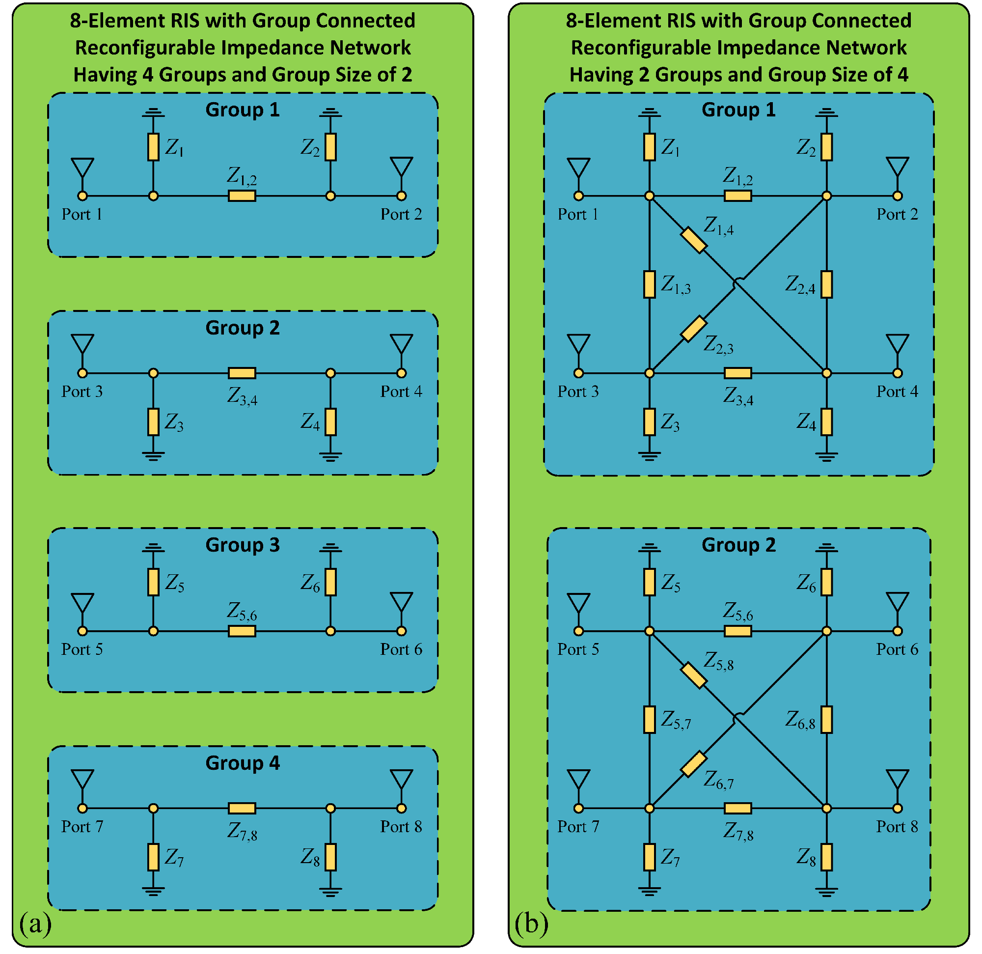
For the fully connected reconfigurable impedance network, when becomes large, the number of reconfigurable impedance components becomes huge (increasing quadratically with ) and the circuit topology will become intricate. This limits its practical use and therefore we also propose a group connected reconfigurable impedance network to achieve a good tradeoff between performance enhancement and complexity. Two illustrative examples, for an 8-element RIS with a group connected reconfigurable impedance network having 4 groups and 2 groups, are shown in Fig. 3(a) and (b), respectively. In Fig. 3(a), the 8 elements in RIS are divided into 4 groups and each group has 2 elements and uses a 2-port fully connected reconfigurable impedance network. In Fig. 3(b), the 8 elements in RIS are divided into 2 groups and each group has 4 elements and uses a 4-port fully connect reconfigurable impedance network. Generally, for -element RIS, we can divide it into groups with each group having elements. We refer to as the group size. For the th group, a -port fully connected reconfigurable impedance network with impedance matrix of is used. Therefore, is a block diagonal matrix given by
| (17) |
Subsequently can be found by (9). According to (9) and [38], is a block diagonal matrix satisfying the constraints
| (18) |
| (19) |
Furthermore, to increase the power scattered by RIS, are purely reactive, i.e. where denotes the reactance matrix of the -port reconfigurable impedance network and . Accordingly, can be found as
| (20) |
so that according to [38] we have equivalent constraints
| (21) |
Therefore, is a block diagonal matrix with each block being a complex symmetric unitary matrix. For an -port group connected reconfigurable impedance network, there are in total reconfigurable impedance components. When the group size , it becomes the single connected reconfigurable impedance network. When the group size , it becomes the fully connected reconfigurable impedance network.
Comparisons between the single connected, fully connected, and group connected reconfigurable impedance networks will be shown in the following sections.
III RIS Aided Communication Model
We have analyzed the fundamental relationships between the incident and reflected waves of the antennas at the transmitter, receiver, and RIS. In this section, we establish the RIS aided communication model based on these relationships.
III-A General RIS Aided Communication Model
We first consider a general RIS aided communication model. Combining (4), (6), and (8), we can relate and in a compact form as
| (22) |
where and are respectively given by
| (23) |
Substituting (1) into (22), we have that
| (24) |
We define and partition as
| (25) |
so that we can find and as
| (26) |
We define the voltage vector at the transmitter as where refers to the voltage across the th transmit antenna. We also define the voltage vector at the receiver as where refers to the voltage across the th receive antenna. With the incident and reflected waves, we can find and as
| (27) |
More details about the relationship between the voltages and the incident and reflected waves of an -port network can be found in the Appendix. Utilizing (4), (6), and (26)-(27), we can relate and by
| (28) |
Defining as the transmit signal and as the receive signal , we can find the channel matrix of the RIS aided wireless communication system as
| (29) |
so that we have (ignoring the additive white Gaussian noise (AWGN) at the receiver). According to (23) and , the submatrice and are functions of , denoted as and , so that from (29) the channel matrix is also a function of , denoted as . Hence, we can optimize to intelligently control the channel and enhance the wireless system performance.
The general communication model (29) includes the effects of impedance mismatching and mutual coupling at the transmitter, RIS, and receiver. However, generally it is difficult to find expressions for and due to the matrix inversion operation. Subsequently, it is difficult to find the expressions of , which makes it difficult to obtain insight into the role of RIS in the communication model and to optimize of RIS. Considering this issue, in the following, we consider a special case to simplify the expression of .
III-B RIS Aided Communication Model with Perfect Matching and No Mutual Coupling
We consider a special case that assumes the antenna arrays at the transmitter, RIS, and receiver are perfectly matched and have no mutual coupling, i.e. , , and . In practice, this assumption can be approximately achieved by individually matching each antenna to the reference impedance and keeping the antenna spacing larger than half-wavelength. It is also assumed that the source impedance at the transmitter and the load impedance at the receiver are all reference impedances so that and . With these two assumptions, we can simplify
| (30) |
so that accordingly we can simplify as
| (31) |
Making use of (30) and (31), we can simplify the expression of and then write that
| (32) | ||||
| (33) |
Substituting (32) and (33) into (29) and making use of and , we can simplify the channel matrix as
| (34) |
The term refers to the second order reflections between the transmitter and RIS and back to the transmitter. However, in most applications, there is no need to consider these second order reflections because the power of the second reflection is extremely small, and is proportional to the square of the pathloss between the transmitter to RIS. Hence, in most applications, we can approximate as without affecting the accuracy, and then simplify as
| (35) |
The transmission scattering matrices , , and are equivalently the channel matrices from the transmitter to receiver, from the transmitter to RIS, and from the RIS to receiver, respectively. To show the equivalence, we consider the impedance matrix of the -port network
| (36) |
Since we assume perfect matching and no mutual coupling, we have and following [38] we can derive
| (37) |
for . We take as an example to see the details. The th entry of , denoted as , refers to the trans-impedance between the th transmit antenna and th receive antenna. To find , we excite the th transmit antenna with current and keep all the other antennas open circuited, and then measure the open-circuit voltage at the th receive antenna. Using the multipath propagation based model, we have that
| (38) |
where and denote the open-circuit radiation pattern of the th transmit antenna and the th receive antenna, respectively. We assume a channel with paths for propagation from transmitter to receiver with the th path characterized by departure and arrival angles and , respectively, and a complex channel gain . Therefore, from (37) and (38), we show that is equivalently the channel matrix from the transmitter to receiver. Similarly, we can show that and are the channel matrices from the transmitter to RIS and from the RIS to receiver, respectively. We use auxiliary notations , , and to facilitate understanding, so that we can rewrite (35) as
| (39) |
Furthermore, assuming there are LoS and non-LoS (NLoS) paths in (38), we can model , , and as Rician fading, i.e.
| (40) |
for where refers to the pathloss, refers to the Rician factor, and represent the small-scale LoS and NLoS (Rayleigh fading) components, respectively.
The simplified (39) is a linear function of and together with
- 1.
the single connected reconfigurable impedance network which satisfies the constraint that ,
- 2.
the fully connected reconfigurable impedance network which satisfies the constraints that , ,
- 3.
the group connected reconfigurable impedance network which satisfies the constraints that , , , ,
make up our proposed RIS aided communication model. Based on this model, we can optimize to intelligently control the channel and enhance the wireless system performance. Note that, the conventional RIS aided communication model used in [7]-[30] is a special case of our proposed model that corresponds to the single connected reconfigurable impedance network. Importantly, in sharp contrast with the conventional single connected architecture [7]-[30] that only adjusts the phases of the impinging waves using a diagonal scattering matrix, our proposed group and fully connected architectures enable scattering matrices to be block diagonal or full and can consequently adjust not only the phases but also the magnitudes of the impinging waves. This leads to significant performance gains in fading channels as it will appear in Sections IV and V.
Remark 1.
It is worthwhile to clarify the differences between our proposed model with the RIS aided communication model proposed in recent work [40]. There are four differences. First, compared with using impedance parameter in [40], we have found it is more natural to use the reflection coefficient and scattering parameter to account for the scattering mechanism of RIS and derive the RIS aided communication model. Second, our general RIS aided communication model (29) includes the effects of impedance mismatching and mutual coupling at the transmitter, RIS, and receiver, which is more general than [40]. Third, we clearly explain the physical significance of the phase shifts and the unit modulus constraint. Fourth, we go beyond the single connected reconfigurable impedance network (the main focus in [40]) and propose more general fully connected and group connected reconfigurable impedance networks.
IV Scaling Law
In order to obtain insights into the fundamental limits of single, fully, and group connected reconfigurable impedance networks in RIS, we quantify how the received signal power scales as a function of the number of RIS elements . For simplicity, we consider a SISO RIS aided system (, ) with perfect matching and no mutual coupling in the following. The transmit signal is with . According to (39), the received signal can be expressed as
| (41) |
where , , and denote the channel from the transmitter to the receiver, from the transmitter to the RIS, and from the RIS to the receiver, respectively, and is the AWGN. For simplicity, we assume the transmit power and omit the direct channel , so that we can express the received signal power as .
IV-A Single Connected Reconfigurable Impedance Network
IV-B Fully Connected Reconfigurable Impedance Network
For the fully connected reconfigurable impedance network (16), using the Cauchy-Schwarz inequality and that , we can find an upper bound for the maximum received signal power as
| (45) |
The key to achieve the upper bound is that we need to find a complex symmetric unitary matrix satisfying
| (46) |
However, it is difficult to derive a closed-form solution for the optimal which satisfies the equation (46) and achieves the upper bound. Hence, we directly optimize to approach the upper bound using the quasi-Newton method as detailed in the next section. Numerical results using the Monte Carlo method confirms that the upper bound (45) is tight.
It is also worthwhile to compare the maximum received signal power of the single connected and fully connected reconfigurable impedance networks. From (44) and (45), using Cauchy-Schwarz inequality we can deduce that
| (47) |
and the equality is achieved if and only if
| (48) |
where can be any positive scalar. In other words, when the channel gains (the modulus) of and are linearly independent, the fully connected reconfigurable impedance network can achieve a higher received signal power than the single connected case.
We also provide physical explanations to account for the better performance of the fully connected case. For the single connected case, each port of the reconfigurable impedance network is not connected to other ports. As a result, only the phase of the elements of the vector can be adjusted. Therefore the best that RIS can achieve is to make the two channel vectors and element-wise in phase. However, for the fully connected case, each port of the reconfigurable impedance network is connected to each other. As a result, the phase and magnitude of the elements of the vector can be jointly adjusted so that the RIS can align the two channel vectors and in the same direction to achieve a better performance. Intuitively speaking, the single connected case is analogous to the equal-gain combining while the fully connected case is analogous to the maximum ratio combining. Namely, instead of adjusting only the phase of the impinging wave as in the single connected architecture, the fully connected architecture can adjust not only the phases but also the magnitudes of the impinging waves.
IV-C Group Connected Reconfigurable Impedance Network
For the group connected reconfigurable impedance network (18), (21), we can rewrite the received signal power as
| (49) |
where with and with . Using the triangle inequality, Cauchy-Schwarz inequality, and that , we can find an upper bound for the maximum received signal power as
| (50) |
The key to achieve the upper bound is that we need to find a complex symmetric unitary matrix satisfying
| (51) |
However, it is difficult to derive a closed-form solution for the optimal achieving the upper bound. Similar to the fully connected case, we directly optimize to approach the upper bound using the quasi-Newton method and numerical results using the Monte Carlo method confirm that the upper bound (50) is tight.
The group connected case can be viewed as a tradeoff between the single connected and fully connected cases so that it is straightforward to show that . In the next subsections, we investigate , , and with LoS and Rayleigh fading channels.
IV-D Line-of-Sight Channel
Assuming and are both LoS channels, we have that and . In this case, it is obvious that the optimal for the single, fully, and group connected reconfigurable impedance networks are the same and given by
| (52) |
Therefore, the single, fully, and group connected reconfigurable impedance networks have the same performance with LoS channel such that
| (53) |
This is consistent with that the equality in (47) that can be achieved when (48) is satisfied.
IV-E Rayleigh Fading Channel
Assuming and are independent and identically distributed (i.i.d.) Rayleigh fading channels, we have and . We first consider the group connected case. We rewrite as
| (54) |
Taking the expectation and making use of the i.i.d. Rayleigh fading assumption of and , we can find the average as
| (55) |
Making use of the moment of distribution, we have that and where refers to the gamma function. With and the expressions of moments, is given by
| (56) |
The single and fully connected reconfigurable impedance networks can be viewed as two special cases of the group connected reconfigurable impedance network, i.e. the group size and . Therefore, from (56), we can straightforwardly derive that
| (57) | ||||
| (58) |
From (57), we can deduce that when , which is consistent with existing results [8] indicating that the RIS has a squared power gain. For the single, group, and fully connected reconfigurable impedance networks, we directly optimize to maximize the received signal power using the quasi-Newton method as detailed in the next section. Using the Monte Carlo method, we optimize for each channel realization and find the average received signal power. The comparisons between the optimized result and the upper bound (or the closed-form solution) for the single, group, and fully connected reconfigurable impedance networks are shown in Fig. 4. We can observe that the optimized average received signal power is the same as the upper bound for the group and fully connected cases, which shows the upper bounds (45) and (50) are tight. Therefore, we can conclude that and .
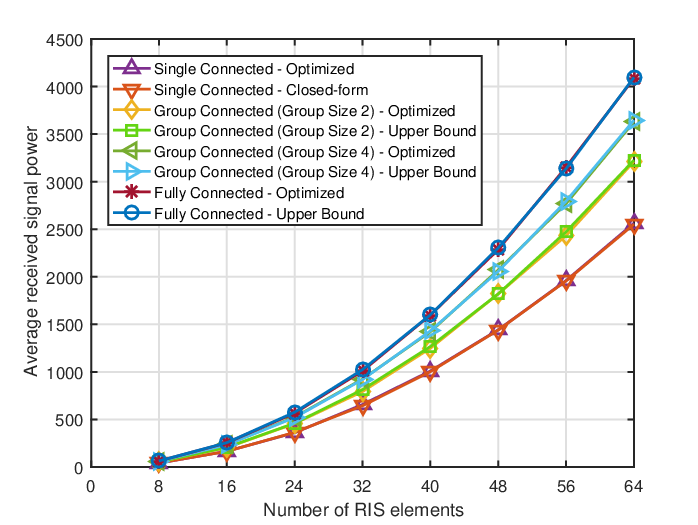
Additionally, we can observe that 1) the group connected case achieves higher average received signal power than the single connected case, 2) the larger the group size is, the higher the average received signal power is, and 3) the fully connected case achieves the highest power. The higher received power of the fully and group connected architectures in Rayleigh fading channel comes from their ability to adjust both the phases and the magnitudes of the impinging waves. To quantify the increase in the received signal power, we can find the power gain of the group and fully connected cases over the single connected case, which are respectively given by
| (59) | ||||
| (60) |
When , the limits of the power gain are
| (61) | ||||
| (62) |
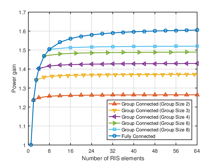
The power gains and versus are shown in Fig. 5. We can observe that the power gain increases with the group size. For , 3, 4, 6, 8, the power gain is around 1.26, 1.37, 1.43, 1.49, 1.52, respectively. However, increasing the group size cannot increase the power gain without limit. For the fully connected case (the maximum group size), we can find that the limit of the power gain is around 1.62, which is consistent with (61). Comparing and , we find that small group size , such as 2, 3, 4, achieves satisfactory power gain while maintaining low complexity. Therefore, the group connected reconfigurable impedance network with small group size is more useful in practice.
Given the same average received signal power, the number of RIS elements required by the group connected or fully connected reconfigurable impedance network (denoted as and ) is less than that required by the single connected reconfigurable impedance network (denoted as ). When the number of RIS elements is large, from (59), we can deduce that
| (63) |
The percentage decrease in the number of RIS elements is given by
| (64) |
which can also be applied to the fully connected case by replacing with . Therefore, for , 3, 4, 6, 8, we have , 14%, 16%, 18%, 19%, respectively. For the fully connected case, we have . Such reduction in the number of RIS elements is beneficial for reducing the cost and area of RIS, especially when the number of RIS elements is large. Similarly, we find for small group sizes , such as 2, 3, 4, they achieve the greatest relative RIS element reduction while maintaining low complexity, demonstrating that the group connected reconfigurable impedance network with small group size is more useful in practice.
To conclude, comparing the performance of the three RIS architectures in LoS and Rayleigh fading channels, we show the gains of fully and group connected cases appear when the channel gains (the modulus) of and are linear independent.
V Performance Evaluation
In this section, we formulate the received signal power maximization in an RIS aided SISO system with the fully connected and group connected reconfigurable impedance networks, and evaluate the performance in a realistic channel model. The received signal power is given by We first consider the group connected reconfigurable impedance network in the RIS, corresponding to the constraints (18), (21). Maximizing is equivalent to maximizing since can always be made in phase with . Therefore, we can equivalently formulate the received signal power maximization problem with the group connected reconfigurable impedance network as
| (65) | ||||
| (66) | ||||
| (67) | ||||
| (68) |
The constraints (66)-(68) indicate that is a block diagonal matrix with each block being a complex symmetric unitary matrix, which makes the optimization difficult. To handle that, we leverage the relationship between the scattering matrix and the reactance matrix , as provided in (20), to equivalently rewrite the problem (65)-(68) as
| (69) | ||||
| (70) | ||||
| (71) | ||||
| (72) |
which can be transformed to an unconstrained optimization problem. Specifically, substituting (70) and (71) into the objective (69), we can express the objective (69) as a function of . Since can be an arbitrary real symmetric matrix, is a function of the entries in the upper triangular part, i.e. for , and there is no constraint for for . Therefore, we can express the objective (69) as a function of for and all . Subsequently we can transform the problem (69)-(72) to an unconstrained problem which optimizes unconstrained variables for and all . To solve the unconstrained optimization problem, we can use the quasi-Newton method in MATLAB to directly optimize for and all , and then find a stationary point of the problem (69)-(72). Using the quasi-Newton method with BFGS update, the computational complexity for each iteration is [41]. The single and fully connected reconfigurable impedance networks can be viewed as two special cases of the group connected reconfigurable impedance network, i.e. the group size and . Therefore, we can follow the same approach to solve the received signal power maximization problem with single and fully connected cases.
We now evaluate the performance of the RIS aided SISO system with the single, fully, and group connected reconfigurable impedance networks. We consider a two-dimensional (2D) coordinate system as shown in Fig. 6. A single-antenna transmitter is located at (0, 0) and a single-antenna receiver is located at (52, 0). A uniform linear array (ULA) at the RIS are located in -axis. The antenna spacing is half wavelength and the center of the array is located at (50, 2). The distance-dependent pathloss model is given by
| (73) |
where refers to the pathloss at the reference distance meter (m), refers to the distance, and refers to the pathloss exponent for . For the small-scale fading, we assume that the transmitter-receiver and RIS-receiver channels are both Rayleigh fading channels, and assume that the transmitter-RIS channel is Rician fading as provided in (40). We set , , , dB, and W.


Using the Monte Carlo method, we compute the average received signal power achieved after optimizing the single, fully, and group connected reconfigurable impedance networks. The average received signal power versus the number of RIS elements with different Rician factors of the transmitter-RIS channel is shown in Fig. 7. We can make the following observations. First, the group connected reconfigurable impedance network achieves a higher received signal power than the single connected reconfigurable impedance network. The fully connected reconfigurable impedance network achieves the highest received signal power. This demonstrates the benefit of the group and fully connected reconfigurable impedance networks. Second, the larger the group size is, the higher the received signal power is, which indicates that we can trade complexity for signal power enhancement. Last, the received signal power of the fully connected reconfigurable impedance network does not change with the Rician factor. Indeed, it can be deduced from the scaling laws (53) and (58) in that the received signal power is always . However, the received signal power of the single connected case increases with the Rician factor. Indeed, we can deduce from the scaling laws (53) and (57) in that the single connected case achieves a higher power in the LoS channel compared to Rayleigh fading channels.
We also plot the power gains of the group and fully connected reconfigurable impedance networks over the single connected reconfigurable impedance network with different Rician factors of the transmitter-RIS channel in Fig. 8. We find that the power gain decreases with the Rician factor. To show the tradeoff between performance and complexity for the single, group, and fully connected reconfigurable impedance networks, we quantify the complexity from two perspectives, 1) the circuit topology complexity, which refers to the number of reconfigurable impedance components in the reconfigurable impedance network, and 2) the optimization computational complexity, which refers to the computational complexity for optimizing the reconfigurable impedance networks with different constraints of . A comprehensive comparison of the single, group, and fully connected reconfigurable impedance networks in terms of the power gain at different Rician factors, the circuit topology complexity, and the optimization computational complexity is summarized in Table. I. We can conclude that the power gain can be enhanced by introducing more reconfigurable components and more optimization computations, i.e. trading circuit topology complexity and optimization computational complexity for performance enhancement. Particularly, the group connected reconfigurable impedance network with group size of 2 achieves a good tradeoff between complexity and performance enhancement, which uses half more reconfigurable impedance components and 1.25 times more computations to improve the received signal power by around 20%. In addition, given the same received signal power, using the group connected reconfigurable impedance network can reduce the number of RIS elements. For example, for the group size of 2 and 4 with Rician factor of 0 dB, the number of RIS elements can be reduced by 9.5% and 13.6%, respectively. Such reduction of the number of RIS elements is beneficial for reducing the cost and area of RIS, especially when the number of RIS elements is large.


| Power Gain | Circuit | Optimization | ||||
| Group Size | Rician | Rician | Rician | Topology | Computational | |
| Factor 0 dB | Factor 3 dB | Factor 10 dB | Complexity | Complexity† | ||
| Single Connected | 1 | 1 | 1 | 1 | ||
| Group Connected | 2 | 1.22 | 1.20 | 1.14 | 1.5 | |
| Group Connected | 4 | 1.34 | 1.31 | 1.21 | 2.5 | |
| Fully Connected | 1.48 | 1.42 | 1.30 | |||
† The computational complexity for each iteration using quasi-Newton method with BFGS update.
VI Conclusions and Future Work
We use scattering parameter network analysis to derive a physical and EM compliant yet straightforward and tractable RIS aided communication model. The proposed general RIS aided communication model fully considers the effects of impedance mismatching and mutual coupling at the transmitter, RIS, and receiver, and thus is more comprehensive than the conventional RIS aided communication model [4], [5], [7]-[30] which does not consider these effects. Furthermore, the proposed general model can be reduced to the conventional RIS aided communication model [4], [5], [7]-[30] under special conditions.
Using the proposed RIS model we also develop new RIS architectures based on group and fully connected reconfigurable impedance networks, which are more general and efficient than previously utilized single connected architecture [4], [5], [7]-[30]. In sharp contrast with the single connected architecture that only adjusts the phases of the impinging waves using a diagonal scattering matrix, our proposed group and fully connected architectures enable scattering matrices to be block diagonal or full and can adjust not only the phases but also the magnitudes of the impinging waves, so as to provide better performance in RIS aided systems.
We derive the scaling law of the received signal power of a SISO RIS aided system as a function of the number of RIS elements in both LoS and Rayleigh fading channels. It shows that using fully and group connected reconfigurable impedance networks can increase the received signal power by up to 62% compared with the single connected case. It also indicates that given the same received signal power, using fully connected and group connected reconfigurable impedance networks can reduce the number of RIS elements by up to 21%. We also formulate the received signal power maximization problem in the SISO RIS aided system and evaluate the received signal power in a realistic model with distance-dependent pathloss and Rician fading channel. The numerical results show that the fully and group connected reconfigurable impedance networks can increase the received signal power by up to 48% and 34%, respectively.
Future research avenues include, but are not limited to, the following areas:
1) Developing efficient channel estimation methods. For the proposed RIS aided communication model with perfect matching and no mutual coupling, the channel matrix (39) is exactly the same as the conventional RIS aided communication model [4], [5], [7]-[30], so that we can use the channel estimation methods for conventional RIS aided communication model [8], [42] to estimate the channel matrix. For the general RIS aided communication model, from the channel matrix expression (29), we need to first measure the impedance mismatch and and mutual coupling , , and by a vector network analyzer and then use the channel estimation methods [8], [42] to estimate the channel matrix. In the future, we can develop more efficient channel estimation methods for the proposed RIS aided communication models.
2) Extending to multi-user and multi-cell scenarios. Previous work on multi-user [8] and multi-cell scenarios [10] only use RIS with the single connected architecture to minimize the transmit power and maximize the weight sum rate, respectively. In the future, we can consider using the fully and group connected architectures, which are more general than the single connected architecture, to further decrease the transmit power in multi-user scenario and increase the weighted sum rate in multi-cell scenario.
3) Optimizing with discrete values of . For the single connected architecture, we have and we can restrict the continuous to discrete values, which is called discrete phase shifts. The optimization with discrete phase shifts has been well studied in [25], [26]. Inspired by the discrete phase shifts, in the future we can consider the design and optimization of discrete values of matrix for the fully and group connected architectures.
Appendix
Scattering parameter network theory [38] is useful to model and analyze wireless systems. This theory has been used to accurately characterize MIMO wireless systems in previous work [37], [43], [44] for example. In this appendix, we briefly review the concept of reflection coefficient and scattering parameters to help provide some background [38].
A. Reflection Coefficient
Consider an arbitrary 1-port network as shown in Fig. 9. The 1-port network can be a source impedance, or a load impedance, or an antenna impedance, and it can be constructed from wires, transmission lines, circuits, antennas, or more generally it can be any linear electromagnetic system [38]. Assume that an incident voltage wave, denoted as , is input into the 1-port network. The incident voltage wave will be reflected by the 1-port network and subsequently a reflected voltage wave, denoted as , is generated. Therefore, the voltage across the port, denoted as , is the sum of the incident and reflected voltage waves, i.e. , and the current through the port, denoted as , is described by where is a chosen reference impedance and usually it is set as . We define the ratio of the reflected and incident voltage waves as the reflection coefficient of the 1-port network, which is denoted as and given by
| (74) |
where denotes the input impedance of the 1-port network. and have a one-to-one correspondence relationship so that can completely characterize any input impedance of a 1-port network. For a passive input impedance , we have that . Particularly, for a pure reactive input impedance , we have that and , which is helpful to increase the power of scattered wave and is the key property of RIS (the phase shift and the unit modulus constraint).
It should also be noted that the reflection coefficient can characterize any 1-port network no matter how it is constructed. Particularly, the reflection coefficient of an antenna characterizes how much of the incident wave the antenna can radiate, which is an important parameter in antenna design for wireless systems.


B. Scattering Parameters
Generalizing the concept of the 1-port network, we consider an arbitrary -port network as shown in Fig. 10, where refers to the wave incident on the th port and refers to the wave reflected from the th port. Denote and . The scattering parameter matrix is defined in relation to these incident and reflected waves as . Similar to the impedance or admittance parameter matrix for an -port network, the scattering parameter matrix can completely characterize the network as seen at its ports. While the impedance and admittance parameter matrices relate the total voltages and currents at the ports, the scattering parameter matrix relates the waves incident on the ports to those reflected from the ports. In particular, at the th port, the voltage and current are related with the incident and reflected waves by and . Therefore, the scattering matrix can be one-to-one converted to the impedance matrix through
| (75) |
For a 1-port network, the scattering matrix reduces to a scalar, which is essentially the reflection coefficient as introduced in Appendix A.
It should be noted that scattering parameters can characterize any -port network. It does not matter if the -port network is constructed from wires, transmission lines, circuits, antennas, or more generally it can be any linear electromagnetic system. Particularly, for SISO wireless systems, the single transmit antenna and single receive antenna embedded in the wireless channel can be viewed as a 2-port network, where the parameter in the scattering matrix is the channel gain between two antennas. Moreover, the scattering parameter network analysis can accurately characterize MIMO wireless systems, as shown in [37], [43], [44]. In practice, scattering parameters can be measured by a vector network analyzer [38] and have been widely used in the measurements of microwave circuit and component, antennas, and wireless systems. To conclude, reflection coefficient and scattering parameters are suitable and accurate for modeling wireless systems.
References
- [1] E. Basar, M. Di Renzo, J. De Rosny, M. Debbah, M. Alouini, and R. Zhang, “Wireless communications through reconfigurable intelligent surfaces,” IEEE Access, vol. 7, pp. 116 753–116 773, 2019.
- [2] S. Gong, X. Lu, D. T. Hoang, D. Niyato, L. Shu, D. I. Kim, and Y.-C. Liang, “Towards smart radio environment for wireless communications via intelligent reflecting surfaces: A comprehensive survey,” arXiv preprint arXiv:1912.07794, 2019.
- [3] Q. Wu, S. Zhang, B. Zheng, C. You, and R. Zhang, “Intelligent reflecting surface aided wireless communications: A tutorial,” arXiv preprint arXiv:2007.02759, 2020.
- [4] Q. Wu and R. Zhang, “Towards smart and reconfigurable environment: Intelligent reflecting surface aided wireless network,” IEEE Communications Magazine, vol. 58, no. 1, pp. 106–112, 2020.
- [5] N. Rajatheva et al., “White paper on broadband connectivity in 6G,” 2020.
- [6] S. Jin, M. R. McKay, C. Zhong, and K. Wong, “Ergodic capacity analysis of amplify-and-forward mimo dual-hop systems,” IEEE Transactions on Information Theory, vol. 56, no. 5, pp. 2204–2224, 2010.
- [7] C. Huang, A. Zappone, G. C. Alexandropoulos, M. Debbah, and C. Yuen, “Reconfigurable intelligent surfaces for energy efficiency in wireless communication,” IEEE Transactions on Wireless Communications, vol. 18, no. 8, pp. 4157–4170, 2019.
- [8] Q. Wu and R. Zhang, “Intelligent reflecting surface enhanced wireless network via joint active and passive beamforming,” IEEE Transactions on Wireless Communications, vol. 18, no. 11, pp. 5394–5409, 2019.
- [9] B. Ning, Z. Chen, W. Chen, and J. Fang, “Beamforming optimization for intelligent reflecting surface assisted MIMO: A sum-path-gain maximization approach,” IEEE Wireless Communications Letters, vol. 9, no. 7, pp. 1105–1109, 2020.
- [10] C. Pan, H. Ren, K. Wang, W. Xu, M. Elkashlan, A. Nallanathan, and L. Hanzo, “Multicell MIMO communications relying on intelligent reflecting surfaces,” IEEE Transactions on Wireless Communications, vol. 19, no. 8, pp. 5218–5233, 2020.
- [11] G. Zhou, C. Pan, H. Ren, K. Wang, and A. Nallanathan, “Intelligent reflecting surface aided multigroup multicast MISO communication systems,” IEEE Transactions on Signal Processing, vol. 68, pp. 3236–3251, 2020.
- [12] Y. Yang, B. Zheng, S. Zhang, and R. Zhang, “Intelligent reflecting surface meets OFDM: Protocol design and rate maximization,” IEEE Transactions on Communications, vol. 68, no. 7, pp. 4522–4535, 2020.
- [13] B. Zheng and R. Zhang, “Intelligent reflecting surface-enhanced OFDM: Channel estimation and reflection optimization,” IEEE Wireless Communications Letters, vol. 9, no. 4, pp. 518–522, 2020.
- [14] B. Zheng, Q. Wu, and R. Zhang, “Intelligent reflecting surface-assisted multiple access with user pairing: NOMA or OMA?” IEEE Communications Letters, vol. 24, no. 4, pp. 753–757, 2020.
- [15] X. Yu, D. Xu, Y. Sun, D. W. K. Ng, and R. Schober, “Robust and secure wireless communications via intelligent reflecting surfaces,” IEEE Journal on Selected Areas in Communications, pp. 1–1, 2020.
- [16] W. Zhao, G. Wang, S. Atapattu, T. A. Tsiftsis, and X. Ma, “Performance analysis of large intelligent surface aided backscatter communication systems,” IEEE Wireless Communications Letters, vol. 9, no. 7, pp. 962–966, 2020.
- [17] Q. Wu and R. Zhang, “Joint active and passive beamforming optimization for intelligent reflecting surface assisted SWIPT under QoS constraints,” IEEE Journal on Selected Areas in Communications, vol. 38, no. 8, pp. 1735–1748, 2020.
- [18] ——, “Weighted sum power maximization for intelligent reflecting surface aided SWIPT,” IEEE Wireless Communications Letters, vol. 9, no. 5, pp. 586–590, 2020.
- [19] X. Guan, Q. Wu, and R. Zhang, “Joint power control and passive beamforming in irs-assisted spectrum sharing,” IEEE Communications Letters, vol. 24, no. 7, pp. 1553–1557, 2020.
- [20] J. Yuan, Y. C. Liang, J. Joung, G. Feng, and E. G. Larsson, “Intelligent reflecting surface-assisted cognitive radio system,” IEEE Transactions on Communications, vol. 69, no. 1, pp. 675–687, 2021.
- [21] L. Ge, P. Dong, H. Zhang, J. Wang, and X. You, “Joint beamforming and trajectory optimization for intelligent reflecting surfaces-assisted UAV communications,” IEEE Access, vol. 8, pp. 78 702–78 712, 2020.
- [22] X. Lu, W. Yang, X. Guan, Q. Wu, and Y. Cai, “Robust and secure beamforming for intelligent reflecting surface aided mmwave miso systems,” IEEE Wireless Communications Letters, vol. 9, no. 12, pp. 2068–2072, 2020.
- [23] J. Qiao and M. S. Alouini, “Secure transmission for intelligent reflecting surface-assisted mmwave and terahertz systems,” IEEE Wireless Communications Letters, vol. 9, no. 10, pp. 1743–1747, 2020.
- [24] T. Bai, C. Pan, Y. Deng, M. Elkashlan, A. Nallanathan, and L. Hanzo, “Latency minimization for intelligent reflecting surface aided mobile edge computing,” IEEE Journal on Selected Areas in Communications, pp. 1–1, 2020.
- [25] J. Xu, W. Xu, and A. L. Swindlehurst, “Discrete phase shift design for practical large intelligent surface communication,” in 2019 IEEE Pacific Rim Conference on Communications, Computers and Signal Processing (PACRIM), 2019, pp. 1–5.
- [26] Q. Wu and R. Zhang, “Beamforming optimization for wireless network aided by intelligent reflecting surface with discrete phase shifts,” IEEE Transactions on Communications, vol. 68, no. 3, pp. 1838–1851, 2020.
- [27] Y. Han, W. Tang, S. Jin, C. Wen, and X. Ma, “Large intelligent surface-assisted wireless communication exploiting statistical CSI,” IEEE Transactions on Vehicular Technology, vol. 68, no. 8, pp. 8238–8242, 2019.
- [28] G. Zhou, C. Pan, H. Ren, K. Wang, and A. Nallanathan, “A framework of robust transmission design for IRS-aided MISO communications with imperfect cascaded channels,” IEEE Transactions on Signal Processing, vol. 68, pp. 5092–5106, 2020.
- [29] C. Huang, R. Mo, and C. Yuen, “Reconfigurable intelligent surface assisted multiuser MISO systems exploiting deep reinforcement learning,” IEEE Journal on Selected Areas in Communications, vol. 38, no. 8, pp. 1839–1850, 2020.
- [30] K. Feng, Q. Wang, X. Li, and C. Wen, “Deep reinforcement learning based intelligent reflecting surface optimization for MISO communication systems,” IEEE Wireless Communications Letters, vol. 9, no. 5, pp. 745–749, 2020.
- [31] Ö. Özdogan, E. Björnson, and E. G. Larsson, “Intelligent reflecting surfaces: Physics, propagation, and pathloss modeling,” IEEE Wireless Communications Letters, vol. 9, no. 5, pp. 581–585, 2020.
- [32] W. Tang, M. Z. Chen, X. Chen, J. Y. Dai, Y. Han, M. Di Renzo, Y. Zeng, S. Jin, Q. Cheng, and T. J. Cui, “Wireless communications with reconfigurable intelligent surface: Path loss modeling and experimental measurement,” IEEE Transactions on Wireless Communications, pp. 1–1, 2020.
- [33] S. Abeywickrama, R. Zhang, and C. Yuen, “Intelligent reflecting surface: Practical phase shift model and beamforming optimization,” in ICC 2020 - 2020 IEEE International Conference on Communications (ICC), 2020, pp. 1–6.
- [34] W. Cai, H. Li, M. Li, and Q. Liu, “Practical modeling and beamforming for intelligent reflecting surface aided wideband systems,” IEEE Communications Letters, vol. 24, no. 7, pp. 1568–1571, 2020.
- [35] E. Björnson and L. Sanguinetti, “Demystifying the power scaling law of intelligent reflecting surfaces and metasurfaces,” in 2019 IEEE 8th International Workshop on Computational Advances in Multi-Sensor Adaptive Processing (CAMSAP), 2019, pp. 549–553.
- [36] E. Björnson, Ö. Özdogan, and E. G. Larsson, “Intelligent reflecting surface versus decode-and-forward: How large surfaces are needed to beat relaying?” IEEE Wireless Communications Letters, vol. 9, no. 2, pp. 244–248, 2020.
- [37] J. W. Wallace and M. A. Jensen, “Mutual coupling in mimo wireless systems: a rigorous network theory analysis,” IEEE Transactions on Wireless Communications, vol. 3, no. 4, pp. 1317–1325, 2004.
- [38] D. M. Pozar, Microwave engineering. John Wiley & Sons, 2009.
- [39] S. Shen and R. D. Murch, “Impedance matching for compact multiple antenna systems in random RF fields,” IEEE Trans. Antennas Propag., vol. 64, no. 2, pp. 820–825, Feb. 2016.
- [40] G. Gradoni and M. Di Renzo, “End-to-end mutual-coupling-aware communication model for reconfigurable intelligent surfaces: An electromagnetic-compliant approach based on mutual impedances,” arXiv preprint arXiv:2009.02694, 2020.
- [41] J. Nocedal and S. Wright, Numerical optimization. Springer Science & Business Media, 2006.
- [42] D. Mishra and H. Johansson, “Channel estimation and low-complexity beamforming design for passive intelligent surface assisted MISO wireless energy transfer,” in ICASSP 2019 - 2019 IEEE International Conference on Acoustics, Speech and Signal Processing (ICASSP), 2019, pp. 4659–4663.
- [43] J. W. Wallace and M. A. Jensen, “Termination-dependent diversity performance of coupled antennas: network theory analysis,” IEEE Transactions on Antennas and Propagation, vol. 52, no. 1, pp. 98–105, 2004.
- [44] B. K. Lau, J. B. Andersen, G. Kristensson, and A. F. Molisch, “Impact of matching network on bandwidth of compact antenna arrays,” IEEE Transactions on Antennas and Propagation, vol. 54, no. 11, pp. 3225–3238, 2006.