Electrically induced strong modulation of magnons transport
in ultrathin magnetic insulator filmsPreprint: APS/123-QED
Abstract
Magnon transport through a magnetic insulator can be controlled by current-biased heavy-metal gates that modulate the magnon conductivity via the magnon density. Here, we report nonlinear modulation effects in 10 nm thick yttrium iron garnet (YIG) films. The modulation efficiency is larger than 40%/mA. The spin transport signal at high DC current density (2.2A/m2) saturates for a 400 nm wide Pt gate, which indicates that even at high current levels a magnetic instability cannot be reached in spite of the high magnetic quality of the films.
I Introduction
Magnons, i.e. the quanta of spin waves, are carriers of information with properties that are attractive for applications Chumak et al. 2015. Magnons propagate in ferro-, ferri, antiferro-, and even paramagnetic electric insulators without Joule heating Kittel 1958; Eshbach 1962; Lebrun et al. 2018; Oyanagi et al. 2019. The ferrimagnet yttrium iron garnet (YIG) is to date the best platform for magnon spintronics due to its low Gilbert damping and high Curie temperature. In YIG, magnons can be excited thermally and electrically and can cover long distances Uchida et al. 2008; Kajiwara et al. 2010; Cornelissen et al. 2015. An electric current in a thin-film platinum contact generates a spin accumulation at the PtYIG interface, which injects magnons into YIG. The latter diffuse into the magnet and when reaching another Pt contact generate a voltage by the inverse spin Hall effect. The non-local resistance can be modulated by a third Pt film, as demonstrated for a 210 nm thick YIG film Cornelissen et al. 2018. This three terminal device is a magnon transistor. The left and right ones inject and detect magnons thus form a source and a drain, respectively. Sending a current though the middle strip or gate modulate the source-drain signal by the magnon density in the transport channel.
Chumak et al. Chumak et al. 2014 achieved magnon transistor action by controlling the magnon scattering in a magnonic crystal by a magnetic field. Our device operates by modulating the magnon conductivity of a YIG thin film electrically. Similar to the Drude formula for electrons, the magnon conductivity
| (1) |
on the magnon density , where is the scattering time and is the effective mass that is governed by the spin wave stiffness .

The present study is motivated by the wish to improve the modulation efficiency of the previous device Cornelissen et al. 2018. This can be achieved simply by a thinner YIG film, since for the same number of injected magnons, the magnon density in the source-drain transport channel should be larger Wimmer et al. 2019. To this end we grew an ultra-thin YIG film by liquid-phase expitaxy with thickness of 10 nm with great case in order to not sacrifice the low Gilbert damping of the thicker film. The observed modulation of the nonlocal signal reaches 200 corresponding to a modulation efficiency per DC current unit exceed 40%/mA, which is 20 times larger than for the 210 nm YIG Cornelissen et al. 2018. A similar enhancement has been reported for a nm thick YIG film grown by pulsed laser deposition and larger Gilbert damping Wimmer et al. 2019. The authors interpret an observed non-linearity in the gate-current dependence in terms of a diverging magnon conductivity by a spin Hall current-induced antidamping of the magnetization dynamics under the gate. Based on the observed dependence of the modulation on the gate width and geometry we believe that the physics is more complicated.
This paper is organized as follows: Section II addresses the device configuration, fabrication details and measurement methods. In Section III, we first compare the nonlocal signals in 10 nm and 210 nm thick YIG films. We then discuss the non-linearities that in contrast to the previous report Wimmer et al. 2019 saturate, discuss other device configurations, and show results of spin Hall magnetoresistance measurements of the PtYIG interface at high gate currents. In Section III, we compare our results with those reported by Wimmer et al. Wimmer et al. 2019.
II Experimental details
The magnon transistors as depicted in Fig. 1 are fabricated on 10 nm thick single crystal yttrium iron garnet (YIG) films. The film is grown by liquid phase epitaxy (LPE) on top of a 500m thickness single crystal (110) gadolinium gallium garnet (GGG, Gd3Ga5O12) substrate at the Université de Bretagne Occidentale in Brest, France. The saturation magnetization is mT. The Gilbert damping parameter of the in-plane magnetized film is . All Pt strips, including the magnon injector, modulator and detector, are sputtered with thickness of 9 nm, patterned by electron beam lithography. TiAu layers with thicknesses of 575 nm are deposited by e-beam evaporation. The center-to-center distance between the injector and detector is 3m. The length and width of the Pt strips for 3 measured devices are listed in Table 1, but we focus on Device 1. Results for a fourth device with 7.9 nm thickness YIG are summarized in Appendix B. The sample is positioned between a pair of magnetic poles and rotated by a step motor. The magnetic field orients the soft magnetization in the film plane at an angle with respect to the Pt strips as shown in Fig. 1.
A low-frequency AC current through the magnon injector with an rms-amplitude of , thereby injecting magnons electrically and thermally. The resulting magnon spin currents are measured as the first and second harmonic signals at the magnon detector with a lock-in technique, respectively. A DC current is applied to the gate in order to modulate the magnon spin conductivity and the corresponding nonlocal signals.
| Device | 1 | 2 | 3 |
|---|---|---|---|
| Length (m) | 80/84/80 | 20/24/20 | 20/24/20 |
| Width (m) | 0.4/0.4/0.4 | 0.4/0.8/0.4 | 0.4/1.2/0.4 |
| (A) | 200 | 500 | 500 |
| (A) | -1.51.5 | -2.02.0 | -2.252.25 |
| ‘ | |||
| at =0 (/m) | 198 | 1044 | 160 |
| Modulation | |||
| efficiency (%/mA) | 40.4 | 87 | 75 |
The observed angle-dependent first harmonic signals of Device 1 are shown in Fig. 2: Colors, from red to blue code the nonlocal signals recorded for from -1500A to +1500A. The white dataset in the center for has a typical dependence, i.e. the product of injection and detection efficiencies Cornelissen et al. 2015. The DC bias modulates the magnitude and the angle dependence much more prominently than for a 210 nm thick YIG film Cornelissen et al. 2018, especially at the largest currents of -/+1500A (the darkest red/blue) and and . The gate annihilates magnons in YIG when the spin accumulation is parallel to the magnetic field but creates them when antiparallel, suppression and enhancing is suppressed, respectively. The DC current enhances the signal by more than a factor of 2. Also the second harmonic signals are strongly modulated by the gate current (not shown), but more difficult to interpret since depending not only on the magnon density but also on the temperature profiles in the magnet. We therefore do not discuss them here.

III Results and Discussion
III.1 Dependence of the nonlocal signals on YIG film thickness
The nonlocal signals for 10 nm (Device 1 in Table 1) and 210 nm thick YIG films with the same injector-to-detector distance (3m) are compared in Table 2. The nonlocal resistances scale with the length of the Pt strips. The ultra-thin gated but unbiased 10 nm YIG sample shows a larger non-local signal than the thick one without gate, even though a passive central gate is a spin sink. This result is consistent with the thickness-dependence reported for films from 100 nm up to 50m Shan et al. 2016, but counterintuitive since a thinner film should have a higher impedance. It cannot be explained by either the magnon chemical potential model Cornelissen et al. 2016 nor viscous magnon flow Ulloa et al. 2019. On the other hand, the second harmonic spin Seebeck signal in 10 nm thick YIG (not shown) is much smaller in the 10 nm than in the 210 nm film. The thickness dependence of the nonlocal magnon transport remains unexplained. We may speculate for example about a the existence of highly efficient surface transport channels that dominate in ultra thin films. The thickness dependence of the nonlocal signal will be discussed in a future paper with more details.
| YIG thickness (nm) | 10 | 210Cornelissen et al. 2015 | |
|---|---|---|---|
| (m-1) | 198 | 140 | |
| (MVA-2m-1) | 0.09 | 1.35 |
III.2 Saturation in the injector/modulator/detector geometry for a 400 nm wide gate
The nonlocal resistances are trigonometric functions of the magnetic field angle that reflect the electrical magnon injection and detection efficiencies Cornelissen et al. 2015. The angle-dependent first-harmonic nonlocal resistances are well described by
| (2) |
where is a charge-spin conversion efficiency parameter of the electric spin injection and detection. In the limit of weak excitation, the magnon spin conductivity depends linearly on the magnon density which is again proportional to the and injection current. We also include a quadratic term that does not depend on the current direction and is caused by Joule heating. Hence
| (3) |
where is the DC current in the modulator, is the magnon spin conductivity at thermal equilibrium, and are parameters that can be fitted to the observations.


We extract the non-local resistances at specific angles from Fig. 2 as a function of , subtracting a constant offset at from the measured that is caused by inductive/capacitive coupling. The signals at the angles are shown in Figs. 3a as well as normalized ones for , , and in Figs. 3b. When A (The current density is A/m2.), in Figs. 3a is to a good approximation a parabolic function of
| (4) |
with A and A2 ( for the normalized data in Figs. 3b). The differences between the observations and the fits of Figs. 3a/b are given in Figs. 3c/d , respectively. The data deviate from the fits at the first threshold current A (current density A/m2). At a second threshold A (current density A/m2) the deviations from the polynomial fits show a maximum that we call an anomaly for convenience. For the parabolic model Eq. (3) predicts an increase of the magnon conductivity by the parabolic term that models the magnon injection by Joule heating. However, deviates from this prediction for i.e. at the same current level as for positive gate currents. The experiments confirm that reversing the magnetic field is equivalent to reversing the current direction. The threshold in Fig. 3d increases with the angle while remains constant. Since with increasing a higher current is required to inject the same number of magnons, appears to be related with the magnon injection process, while is not.
III.3 External field dependence of the saturation


A field-dependent study can shed light on the possible effect of the magnon gap or Kittel frequency
| (5) |
on the anomaly . The results in Fig. 4 show a slightly increased with field from 700A to 1 mA. This could reflect a gap-induced reduction of the magnon number and conductivity. which we found to not depend on the magnetization angle above, remains also resilient against the magnetic field strength, however.
III.4 Spin Hall magnetoresistance of the 400 nm wide Pt strip

Next, we analyze the spin Hall magnetoresistance (SMR) of the 400 nm wide Pt center gate Chen et al. 2018 for an AC current of 20 A and a DC current range from -590 A to 590 A. Fig. 5 shows that the resistance change decreases with DC current with a threshold around A, close to introduced above. Since the SMR decreases with temperature Vélez et al. 2016 and appears to be correlated with the first threshold in the non-local signal could be heat-induced, consistent with its independence on the magnetic field reported above.
III.5 Exchanged source and gate contacts


In order collect more information on the anomalies observed in Figs. 3 we exchange roles of the Pt contacts from an injector/modulator/detector to a modulator/injector/detector geometry in Device 1 as sketched in Figs. 6b and specified in Table 3. In this configuration the source-drain current is not directly affected by an antidamping torque of the modulator. The signal is larger because the injector and detector are now closer to each other. The first harmonic signal for the new configuration in Fig. 7 is well represented by a parabola with A and A2 in Eq. (4) for A. () start to decreases for at currents A (1400A) and A (-900A). In contrast to the discussion above, the deviations from the parabolic fit at are negative so we cannot identify a .
In the modulator/injector/detector geometry, magnons injected by the modulator first have to diffuse to the region between the injector and detector in order to affect the magnon conductivity. The magnon chemical potential is a direct measure of the non-equilibrium magnon density that obeys the spin diffusion equation Cornelissen et al. 2015 with a magnon diffusion length of at room temperature. The magnon density in the source-drain channel amounts of the side-modulator geometry should reduced to about 80% of the value for the center gate configuration. A larger current must be therefore be applied to achieve the same magnon density. The additional heating may explain the reduced performance.
| Length (m) | 20/24/20 | |||
|---|---|---|---|---|
| Width (m) | 0.4/0.8/0.4 | |||
| Pt thickness (nm) | 9 | |||
| (A) | 500 | |||
| (A) | -1.61.7 | |||
| Modulation efficiency (%/A) | 23.5 |
III.6 Modulator gate width dependence
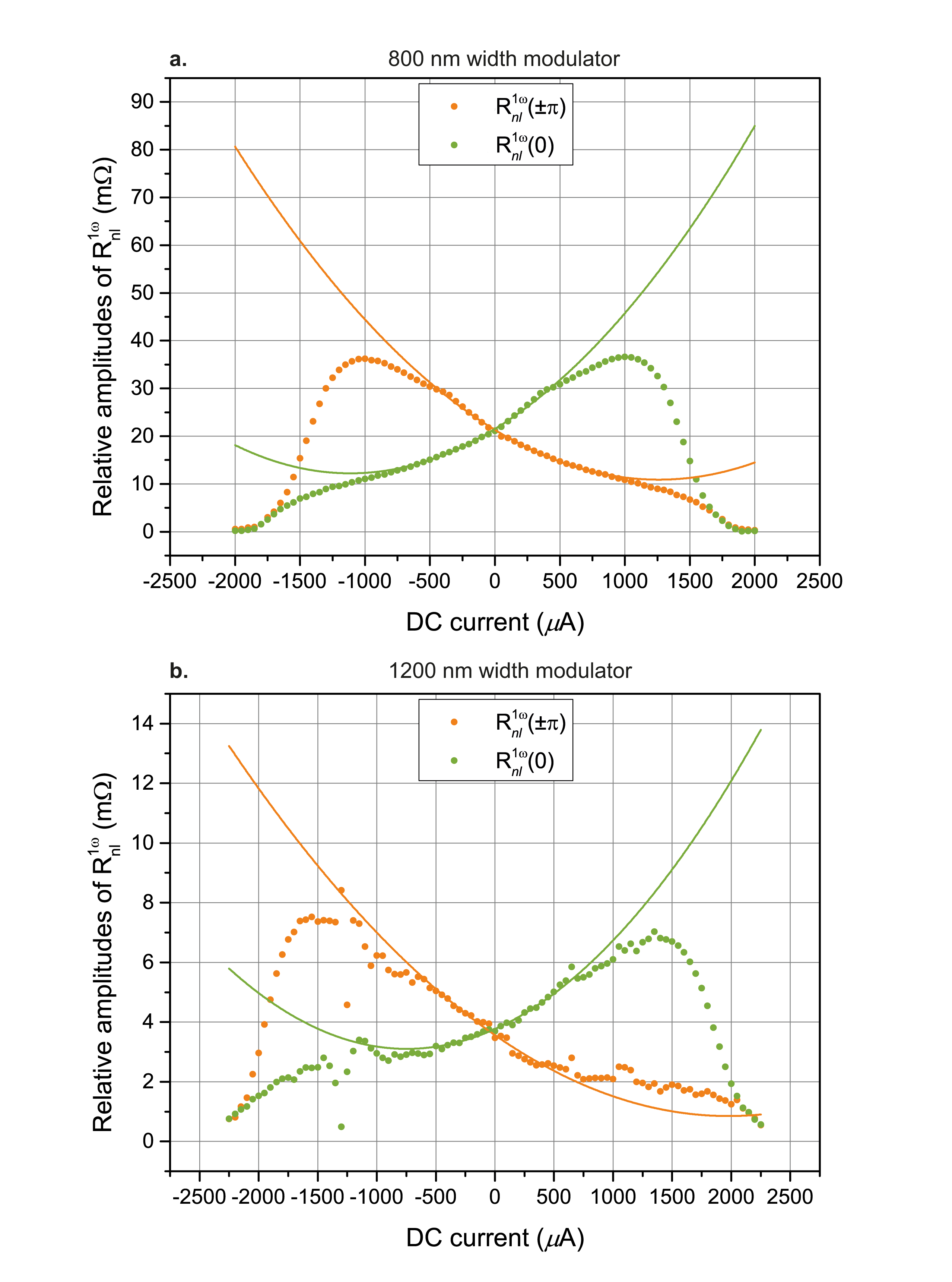
In Device 2 (800 nm wide modulator) and Device 3 (1200 nm wide modulator) from Table I (see Fig. 8), a saturation as in Device 1 (Fig. 3a) is not observed. The characteristics are similar to that of Device 1 in the modulator/injector/detector configuration: deviates from the simple magnon conductivity model at lower currents. Device 2 deviates at currents (current densities) of 500 (A/m2) and starts to decrease at 1 mA (A/m2). Device 3 deviates from A/m2 and starts to decrease at A/m2. They are much lower than the current density corresponding to the saturation in Device 1 (A/m2). How the width of the gate affects the nonlinear effect also needs further investigation.
We also observe signal changes induced by a high DC current bias on Device 3 (see Appendix A) that indicate a transient change of the magnetic order of the YIG film that may also cause the asymmetry between the data in Fig. 8 for flipped current and magnetization directions. Rather than blowing the sample up, we observed a strong increase of the non-local signals. Since we have not been able to explain or repeat these results we do not discuss them in the main text.
IV Discussion and conclusions
We report large modulations of nonlocal magnon transport in a 10 nm thick YIG film by a DC current through a Pt gate. For the injector/modulator/detector geometry, a threshold current separates the low and high DC current regimes. The enhancement of the magnon transport at currents indicates interesting physics such as current-induced self-oscillations of the magnetic order. However, instead of a divergence that could indicate magnon superfluidity, we observe a plateau at high current levels Figs. 3a.
The differences between the data and a parabolic fit at low injection currents sheds some light on what is happening. We clearly observe non-parabolicities for both positive and negative currents, i.e. for both magnon injection and extraction. At the signal is enhanced, i.e. increases above the parabolic fit. This threshold is not sensitive to applied magnetic fields and angles, which indicates a thermal (spin Seebeck) mechanism for the enhancement of the conductivity as reported by C. Safranski et al. Safranski et al. 2017. The SMR data are suppressed around thereby supporting the hypthesis that Joule heating affects the spin-transport at the interface. The residue of the polynomial fit in Figs. 3c shows a maximum, i.e. a peak at the threshold current (in one current direction), and then decreases again. We cannot pinpoint the process that suppresses the magnon conduction at high current levels to a certain mechanism, but it appears to be spin-dependent since in contrast to , depends strongly on the magnetic field strength and direction.
When the modulator is in the center, the magnon transmission is affected by thermal Padrón-Hernández et al. 2011; Bender and Tserkovnyak 2016 or electric Hamadeh et al. 2014; Collet et al. 2016 spin-orbit torques as well as spin absorption by the Pt gate. The situation is simplified for the modulator/injector/detector geometry in so far that the modulator is only a source of additional magnons that increase the injector-detector conductance. is larger for this configuration, presumably because the higher current level is required to generate the same density in the source-drain channel by magnon diffusion. However, in contrast to the center-gate configuration, the signal always stays under the parabolic fit. This indicates that the magnon density is not the only parameter relevant for magnon transport, confirming that a spin Seebeck torque from the Pt interface plays an essential role.
Naively, we expected that for equal current densities the results should not depend on the width of the gate. Nevertheless we find that widening the central gates only decreases the signals relative to the polynomial fit. A proper explanation of this result requires more research.
Summarizing, we observe a threshold behavior at currents that indicates that the film under the gate approaches an instability, confirming previous reports. The threshold does not depend on the magnetization direction and therefore the spin Hall injection, which could indicate an enhancement of the magnon density by the spin Seebeck effect. However, at negative currents the magnon accumulation remains suppressed which indicates that the spin Hall effect injection dominates the spin Seebeck effect. At even higher currents another effect kicks in that suppresses the magnon density and conductivity again. This process is roughly symmetric in the current direction and may be assigned to a non-linear magnon decay into phonons at elevated temperatures.
Wimmer et al. Wimmer et al. 2019 also report non-linear effects induced by a Pt gate current on magnon transport. Their sample is slightly thicker with 13.5 nm with a damping of which is significantly higher than our . They report two anomalies ( and ). The first appears to agree with our and results for agree qualitatively with our data and the magnon conductivity Eq. (3). The current densities correspondig to (A/m2) and (A/m2) are much higher than our (A/m2) and (A/m2). They do not report transport for opposite gate current direction and the associated suppression of the non-local signals, however. For , Wimmer et al. Wimmer et al. 2019 observe signals that increases faster than the parabolic fit, which we confirm here. However, they do not find the saturation we report in Figs. 3a. Wimmer et al. Wimmer et al. 2019 interpret the monotonic increase of their results as an incipient divergence by an anti-damping spin-orbit torque that compensates the damping in the YIG film under the gate and speculate about lossless magnon transport at the onset of self-oscillations or superfluidity. On the other hand, the larger Gilbert damping in their samples could imply that the magnon densities at their highest current levels is significantly lower than ours, so they do not reach the saturation regime that we report here.
Concluding, before drawing conclusion about the nature of nonlinearities, the complications due to heating should be figured out in more detail Thiery et al. 2018; Qin et al. 2017; Geprägs et al. 2016; Nambu et al. 2020. It would be valuable to assess the magnon spin accumulation profile governed by the temperature gradient Shan et al. 2017, which may be different in thin and thick films. We conclude that ultrathin YIG films are a great platform for the research on magnon transport in nonlinear regime, but much work has still to be carried out before magnon Bose-Einstein condensation or superfluidity by electric or thermal spin injection can be confirmed.
V Acknowledgments
We acknowledge the helpful discussion with T. Yu and technical support from J. G. Holstein, H. M. de Roosz, H. Adema T. Schouten and H. de Vries. This work is part of the research program Magnon Spintronics (MSP) No. 159 financed by the Foundation for Fundamental Research on Matter (FOM), which is part of the Netherlands Organisation for Scientific Research (NWO), and supported by the research programme Skyrmionics with project number 170, which is financed by the Dutch Research Council (NWO). The support by NanoLab NL is also gratefully acknowledged. G.B. was supported by JSPS Kakenhi Grant 19H006450.
References
- Chumak et al. (2015) A. V. Chumak, V. I. Vasyuchka, A. A. Serga, and B. Hillebrands, Nature Physics 11, 453 (2015).
- Kittel (1958) C. Kittel, Phys. Rev. 110, 1295 (1958).
- Eshbach (1962) J. R. Eshbach, Phys. Rev. Lett. 8, 357 (1962).
- Lebrun et al. (2018) R. Lebrun, A. Ross, S. A. Bender, A. Qaiumzadeh, L. Baldrati, J. Cramer, A. Brataas, R. A. Duine, and M. Kläui, Nature 561, 222 (2018).
- Oyanagi et al. (2019) K. Oyanagi, S. Takahashi, L. J. Cornelissen, J. Shan, S. Daimon, T. Kikkawa, G. E. W. Bauer, B. J. van Wees, and E. Saitoh, Nature Communications 10, 4740 (2019).
- Uchida et al. (2008) K. Uchida, S. Takahashi, K. Harii, J. Ieda, W. Koshibae, K. Ando, S. Maekawa, and E. Saitoh, Nature 455, 778 (2008).
- Kajiwara et al. (2010) Y. Kajiwara, K. Harii, S. Takahashi, J. Ohe, K. Uchida, M. Mizuguchi, H. Umezawa, H. Kawai, K. Ando, K. Takanashi, S. Maekawa, and E. Saitoh, Nature 464, 262 (2010).
- Cornelissen et al. (2015) L. J. Cornelissen, J. Liu, R. A. Duine, J. Ben Youssef, and B. J. van Wees, Nature Physics 11, 1022 (2015).
- Cornelissen et al. (2018) L. J. Cornelissen, J. Liu, B. J. van Wees, and R. A. Duine, Phys. Rev. Lett. 120, 097702 (2018).
- Chumak et al. (2014) A. V. Chumak, A. A. Serga, and B. Hillebrands, Nature Communications 5, 4700 (2014).
- Wimmer et al. (2019) T. Wimmer, M. Althammer, L. Liensberger, N. Vlietstra, S. Geprägs, M. Weiler, R. Gross, and H. Huebl, Phys. Rev. Lett. 123, 257201 (2019).
- Shan et al. (2016) J. Shan, L. J. Cornelissen, N. Vlietstra, J. Ben Youssef, T. Kuschel, R. A. Duine, and B. J. van Wees, Phys. Rev. B 94, 174437 (2016).
- Cornelissen et al. (2016) L. J. Cornelissen, K. J. H. Peters, G. E. W. Bauer, R. A. Duine, and B. J. van Wees, Phys. Rev. B 94, 014412 (2016).
- Ulloa et al. (2019) C. Ulloa, A. Tomadin, J. Shan, M. Polini, B. J. van Wees, and R. A. Duine, Phys. Rev. Lett. 123, 117203 (2019).
- Chen et al. (2018) Y. Chen, D. Roy, E. Cogulu, H. Chang, M. Wu, and A. D. Kent, Applied Physics Letters 113, 202403 (2018), https://doi.org/10.1063/1.5053120 .
- Vélez et al. (2016) S. Vélez, A. Bedoya-Pinto, W. Yan, L. E. Hueso, and F. Casanova, Phys. Rev. B 94, 174405 (2016).
- Safranski et al. (2017) C. Safranski, I. Barsukov, H. K. Lee, T. Schneider, A. A. Jara, A. Smith, H. Chang, K. Lenz, J. Lindner, Y. Tserkovnyak, M. Wu, and I. N. Krivorotov, Nature Communications 8, 117 (2017).
- Padrón-Hernández et al. (2011) E. Padrón-Hernández, A. Azevedo, and S. M. Rezende, Phys. Rev. Lett. 107, 197203 (2011).
- Bender and Tserkovnyak (2016) S. A. Bender and Y. Tserkovnyak, Phys. Rev. B 93, 064418 (2016).
- Hamadeh et al. (2014) A. Hamadeh, O. d’Allivy Kelly, C. Hahn, H. Meley, R. Bernard, A. H. Molpeceres, V. V. Naletov, M. Viret, A. Anane, V. Cros, S. O. Demokritov, J. L. Prieto, M. Muñoz, G. de Loubens, and O. Klein, Phys. Rev. Lett. 113, 197203 (2014).
- Collet et al. (2016) M. Collet, X. de Milly, O. d’Allivy Kelly, V. V. Naletov, R. Bernard, P. Bortolotti, J. Ben Youssef, V. E. Demidov, S. O. Demokritov, J. L. Prieto, M. Muñoz, V. Cros, A. Anane, G. de Loubens, and O. Klein, Nature Communications 7, 10377 (2016).
- Thiery et al. (2018) N. Thiery, V. V. Naletov, L. Vila, A. Marty, A. Brenac, J.-F. Jacquot, G. de Loubens, M. Viret, A. Anane, V. Cros, J. Ben Youssef, N. Beaulieu, V. E. Demidov, B. Divinskiy, S. O. Demokritov, and O. Klein, Phys. Rev. B 97, 064422 (2018).
- Qin et al. (2017) H. J. Qin, K. Zakeri, A. Ernst, and J. Kirschner, Phys. Rev. Lett. 118, 127203 (2017).
- Geprägs et al. (2016) S. Geprägs, A. Kehlberger, F. D. Coletta, Z. Qiu, E.-J. Guo, T. Schulz, C. Mix, S. Meyer, A. Kamra, M. Althammer, H. Huebl, G. Jakob, Y. Ohnuma, H. Adachi, J. Barker, S. Maekawa, G. E. W. Bauer, E. Saitoh, R. Gross, S. T. B. Goennenwein, and M. Kläui, Nature Communications 7, 10452 (2016).
- Nambu et al. (2020) Y. Nambu, J. Barker, Y. Okino, T. Kikkawa, Y. Shiomi, M. Enderle, T. Weber, B. Winn, M. Graves-Brook, J. M. Tranquada, T. Ziman, M. Fujita, G. E. W. Bauer, E. Saitoh, and K. Kakurai, Phys. Rev. Lett. 125, 027201 (2020).
- Shan et al. (2017) J. Shan, L. J. Cornelissen, J. Liu, J. Ben Youssef, L. Liang, and B. J. van Wees, Phys. Rev. B 96, 184427 (2017).
Appendix A Signal change after gate measurement
Device 3 underwent a transient change after applying a high DC current to the gate. The signal became symmetric around zero angle and enhanced for both 0 and 180 degrees, see Fig. 9, indicating an unidentified thermal mechanism. After this experiment, the nonlocal signal at zero gate current increased by a factor five as shown in Fig. 10. The high DC current appeared to change the properties of YIG under the gate. However, after about two weeks, the characteristics of Device 2 returned back to normal as shown in Fig. 8b.


Appendix B Modulation effect on 7.9 nm thick YIG
We also study a transistor structure on a 7.9 nm thick YIG with damping parameter of . The device parameters are shown in Table 4. Compared to the 10 nm thick YIG, we observe in Fig. 11 a modulation increased by a factor of 3 instead of 2. We have to apply a higher DC currents to reach the nonlinear regime but still observe a saturation at the highest currents.
| Length (m) | 20/25/20 | |||
|---|---|---|---|---|
| Width (m) | 0.4/0.4/0.4 | |||
| Pt thickness (nm) | 8 | |||
| (A) | 200 | |||
| (A) | -1.751.75 | |||
| Distance between centers of Pt (m) | 1.5 |
