Non-universal Scaling of Thermoelectric Efficiency in 3D and 2D Thermoelectric Semiconductors
Abstract
We performed the first-principles calculation on common thermoelectric
semiconductors , , , and in bulk three-dimension (3D) and two-dimension (2D). We found that miniaturization of materials does not generally increase the thermoelectric figure of merit () according to the Hicks and
Dresselhaus (HD) theory. For example, values of 2D (0.32) and 2D (0.04) are smaller than their 3D counterparts (0.49 and 0.09, respectively). Meanwhile, the values of 2D
(0.57) and 2D (0.43) are larger than the bulks (0.54 and 0.18, respectively), which agree with HD theory.
The HD theory breakdown occurs because the band gap and
band flatness of the materials change upon
dimensional reduction.
We found that flat bands give a larger electrical conductivity () and electronic thermal conductivity () in 3D materials, and smaller values in 2D materials.
In all cases, maximum values increase proportionally with the band gap and saturate for the band gap above .
The 2D and obtain a higher due to the flat corrugated bands and narrow peaks in their DOS. Meanwhile, the 2D PbTe violates HD theory due to the flatter bands it exhibits,
while 2D SiGe possesses a small gap Dirac-cone band.
1 Introduction
Thermoelectric (TE) materials are useful for generating electricity from waste heat without any moving parts. Despite decades of research in this field, TE efficiency remains low and stagnant at 10%. This efficiency corresponds to a dimensionless figure of merit () that equals to unity, which is defined as
| (1) |
where is the Seebeck coefficient, is the electric conductivity, is the electronic thermal conductivity, is the phonon thermal conductivity, and is the effective temperature. High electric conductivity is needed to obtain a high value, but increasing it also increases the thermal conductivity, following the Wiedemann-Franz law , where is the Lorenz number. This proportionality reduces value. It is hard to achieve a value over unity due to this relation.
Another factor that reduces the further is the fact that metals exhibit a low Seebeck coefficient, while insulators have the opposite characteristics. Thus good TE materials usually come from semiconductor materials. There exists a range of band gaps [1, 2] and band widths [3] which give the optimal value.
One way to push value beyond unity is through the miniaturization of materials as initially proposed by Hicks and Dresselhaus (HD) [4, 5]. The density of states in 2D and 1D materials show sharp steps and the Van Hove singularities, respectively, which are responsible for the increase of the Seebeck coefficient and hence the value as well. The breakthrough of values has been observed in 1D and 2D nanostructured materials, such as hierarchical PbTe [6], silicon nanowires [7], nanostructured BiSbTe [8]. However, the enhancement due to miniaturization of materials only works when the confinement length is smaller than its thermal de Broglie wavelength [9]. With recent advances in crystal growing of 2D materials, it is possible to have one or few atoms-thick 2D materials that satisfy small confinement lengths.
Moreover, HD theory simply assumes parabolic bands that retain the same band gaps and band flatness as the dimension changes. In reality, these quantities strongly depend on the geometry and the dimension of the materials, and as a result, they will affect TE transport. In this paper, we investigate several common semiconductors TE to check the limitation of the HD theory.
We investigate the 3D and the 2D structures of , , and . The TE properties were calculated by using the first-principles calculation and the Boltzmann transport equation. Additionally, these results can be compared with a simple two-band model to understand the dependence of TE properties on dimensionality, band gap, and band flatness. While the bulk states of these materials are considered as good TE materials, the TE properties of the 2D structures remain in early-stage research. The single quintuple layer (QL) of and have been experimentally fabricated through exfoliation [10, 11]. In the recent study [12], it has been shown that the (001) PbTe monolayer turns into a 2D topological crystalline insulator while SiGe has a graphene-like structure on its 2D surface (siligene) [13].
Our results show that dimension reduction changes the band gaps and the flatness of the band. From the analysis of the two-band model, we show that the band flatness keeps the Seebeck coefficient intact and reduces the and values in 2D materials, while in 3D materials, it increases and due to the different density of states. Overall, the maximum values increase proportionally with band gap and saturate when band gap above in both the 2D and 3D materials. As a result, 2D PbTe, which exhibits relatively flat bands, and 2D SiGe, which has a low band gap, have a low value, and violate HD theory. On the other hand, and agrees with HD theory because of their flat corrugated bands [14] and a lot of narrow peaks on the DOS giving an enhancement in their values. Our results also show that the values of the investigated materials increase as the temperature increase, except for .
2 Methods
We used Quantum Espresso [15] to perform all density functional theory (DFT) calculations with the projected augmented wave (PAW) method [16]. The generalized-gradient approximation (GGA) of Perdew-Burke-Ernzerhof (PBE) functional was used as the exchange-correlation [17]. The plane wave’s cutoff energy and the charge density were set to 60 Ry and 720 Ry, respectively. The Monkhorst-Pack scheme [18] was used to integrate the Brillouin zone in the self-consistent calculations with a k-point mesh of 10 x 10 x 10 for the bulk materials and 10 x 10 x 1
| Material | ||
|---|---|---|
| 2.8 | 1.37 | |
| 0.7 | 1.00 | |
| 1.1 | 2.15 | |
| 0.8 | 4.60 |
for the 2D materials. A vacuum layer of 35 Å is used for the 2D calculations. The convergence criteria for structure optimization was taken to be less than eV and less than eV for the total energy and the total force, respectively.
The semi-classical Boltzmann equations encoded in the BoltzTraP program was used to evaluate the transport properties [19]. To give a better result, a denser k-mesh of 40 x 40 x 40 and 80 x 80 x 1 were used for the bulk materials and the 2D materials, respectively. Relaxation time ( ) and phonon thermal conductivity () were required to evaluate the dimensionless figure of merit () of a material. The values presented in Table 1 are obtained by using the method described in Appendix A of Supplementary Material [20] for all bulk materials. We employed the same values to the corresponding 2D materials.
3 Results and Discussion
3.1 Structural Properties
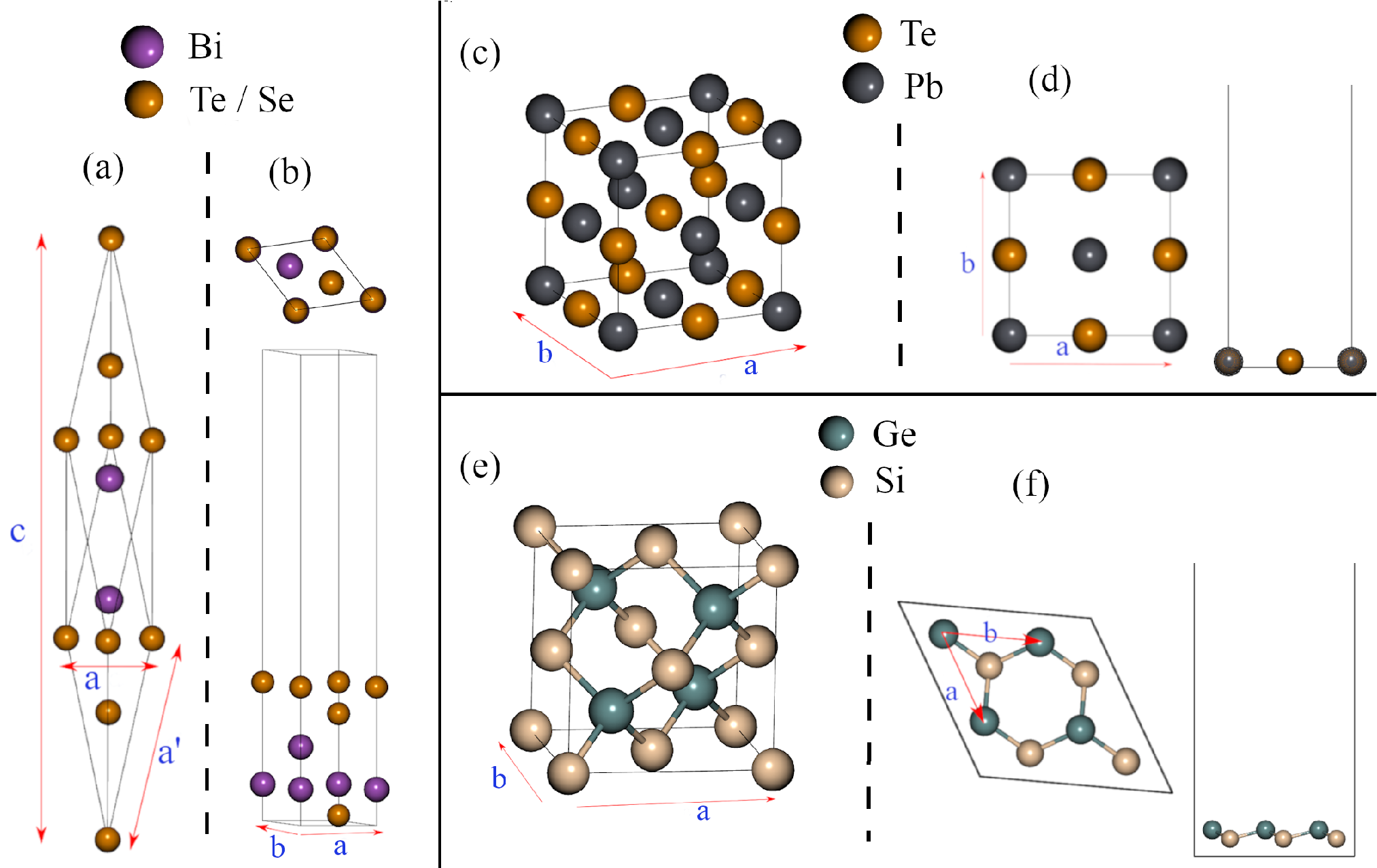
The phase groups of the materials that we used are as follow, R3m for and , Fm3m for , and F43m for . As for the 2-dimensional structures, the quintuple layer (QL) of and , and (001) surface layer of and were used. In this study we only investigated a single layer of each materials. All of the structures are presented in Fig. 1.
The results of our structure optimization are shown in Table. 3 of Supplementary Material. The error between our results and the experiment values are less than 2 %. A further reduction in error could be obtained by using tighter convergence criteria. Bulk and both have the same hexagonal close-packed (HCP) crystal structure. Bulk PbTe has a NaCl face-centered cubic crystal structure. The surface of PbTe in (001) direction possesses a similar lattice constant with the bulk structure, although it is stated in [21] that the lattice constant of (001) few-layers decreases drastically, but the magnitude is unclear for the monolayer PbTe. The (001) surface of SiGe (siligene) has a similar structure with graphene. Nevertheless, unlike planar graphene, siligene possesses a buckling structure. The calculated buckling amplitude is 0.58 Å, which agrees with the previous theoretical work [22].

3.2 Electronic Structure
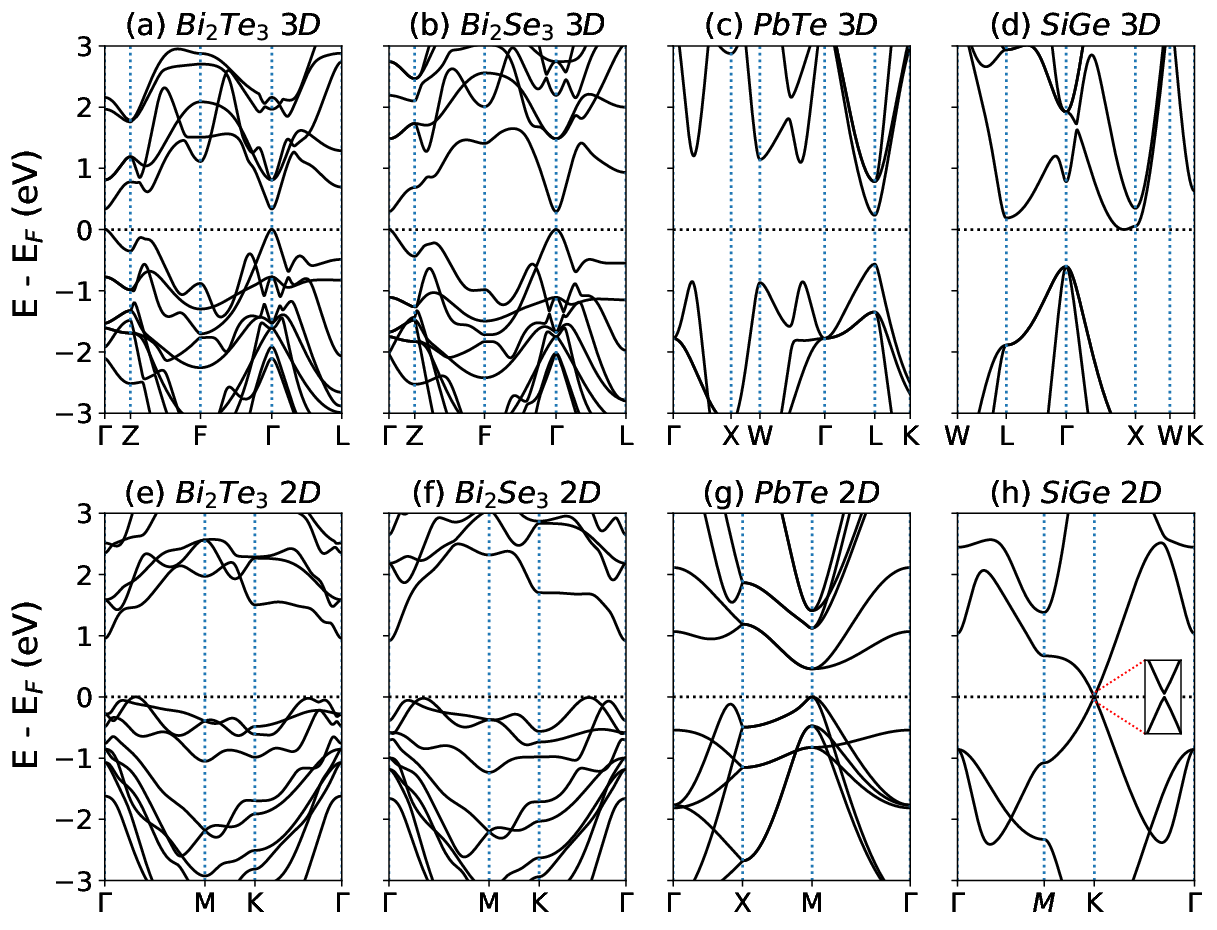
The calculated electronic band structures of each material are shown in Fig. 2. All bulk materials except SiGe have direct band gaps, while for the 2D counterparts, only PbTe and SiGe have the direct band gaps. The siligene exhibits a Dirac cone-shaped band structure at the K point, which was previously found in [13] and [22]. and possess a similar band structure due to their similarity in structure. The band structure of both materials in bulk has a direct band gap at -point, while the inclusion of spin-orbit coupling (SOC) causes a band inversion [23]. As for the single QL, the band structure of without the inclusion of SOC is similar to the previous theoretical calculation [24], where SOC was included.
The band gap values of each material are presented in Table 2. Comparing with the references, we can see that the inclusion of SOC reduces the conduction band energy, especially in materials consisting of heavy atoms. The band energy reduction results in the lowering of the band gap and band inversion in some cases, like . SOC does not affect SiGe tremendously because is composed of light atoms. We note that the GGA underestimates the semiconductor band gaps, which raises a discrepancy between this work and the reference that uses the GGA+U method. The total density of states (DOS) for all materials are shown in Fig. 3. The energy is shifted to the valence band maximum to set it as the reference. In all cases, the DOS near the valence band edge is larger and denser for the 2D structures than the bulk.
3.3 Thermoelectric Properties
The calculated Seebeck coefficients as a function of chemical potential at 300 K are shown in Fig. 4. This study focuses only on longitudinal transports to compare the bulk with the two-dimensional properties. The properties of all materials are isotropic. The chemical potential is related to the carrier concentration. Increasing the chemical potential or carrier concentration way above the gap will decrease the Seebeck coefficient.
The single QL of and have a higher Seebeck coefficient compared to the bulk properties. On the contrary, the bulk properties of SiGe and have a much higher Seebeck coefficient than the 2D counterparts. Single QL of achieved the highest Seebeck coefficient for the 2D materials and PbTe exhibits the highest Seebeck coefficient for the 3D materials, with a value of and respectively.
The second row of Fig. 4 shows the calculated electrical conductivity as a function of chemical potential at 300K. Unlike the Seebeck coefficient, increasing the chemical potential results in the increase of electrical conductivity. P-type has the highest bulk electrical conductivity () while n-type PbTe has the highest conductivity among the 2D materials (). has the smallest magnitude of electrical conductivity. Overall, the electrical conductivities of the 2D structures are lower compared to their bulk structures.

The calculated electronic thermal conductivities are shown in the third row of Fig. 4. Comparing with electrical conductivity, the thermal conductivity of each material has similar trends. From the second and third row, we can see that the increase of electrical conductivity also increases electronic thermal conductivity, which aligns with the Wiedemann-Franz law.
The values are shown in the last row of Fig. 4. We can see that SiGe has the lowest maximum values, which are around 0.09 for the n-type bulk SiGe and 0.04 for the p-type 2D SiGe. The low value in bulk SiGe is due to the high phonon thermal conductivity that it exhibits. The single QL of and achieves a higher maximum value than the bulk structure. The highest value is achieved by p-type on its bulk () and 2D structure (). The 2D materials do not necessarily improve the value. and get the enhancement due to the enhancement in their Seebeck coefficients, while there are materials with lower values than its bulk structure such as SiGe and PbTe.

The band flatness and the band gap are changed upon dimensional reduction, as seen in Fig. 2. To investigate the effects they have on transport properties, we calculate the transport properties using a two-band model, with a Kane band as the conduction band and a parabolic band as the valence band to emulate the asymmetrical bands near the Fermi level. The formulation can be seen in Appendix B of Supplementary Material, and the results are shown in Fig. 5, Fig. 6 and Fig. 10 - 12 in Supplementary Material.
From this simple model, we can see that band flatness gives a positive enhancement to the TE properties in 3D material while it has a detrimental effect on 2D material. Changing the band flatness will only affect the Kane band in CB, thus we only plot vs band gap for n-doped only (Fig. 6). Band flatness does not affect the Seebeck coefficient significantly, but rather it affects and more (Fig. 10 - 12). In 2D systems, and decrease as the band becomes flatter while the Seebeck coefficient remains the same. As a result, the in 2D materials possessing a flat band is lower than those with a more dispersive band. On the contrary, band flatness has the opposite effect on TE properties in 3D due to different DOS. Aside from band flatness, the asymmetrical effective mass parameter described in Ref. [29] might affect TE properties. However, in this work, we assume the masses to be the same. This ratio only affects the 3D systems and has no effects on the 2D, because there is no mass terms in the 2D TE integral (Eq. 18-21 of Supplemental Material).
In general, the maximum value () increases proportionally with the band gap in both the 3D and 2D materials. The maximum values increase as the band gap widens up to a certain threshold value, which is around or 0.25 eV at room temperature, and become saturated beyond this value. The optimum band gap that we obtain is the same as the previous works [1, 2].
From our two band model, we can explain the first-principles calculation results. The 2D PbTe has a low value because it possesses flat bands near its band edge, while 2D SiGe has a low band gap resulting in a low . On the other hand, and bands are corrugated near the Fermi level and are not classified as the flat band as described by the Kane model, so the results from our model cannot be used to describe these materials. The Corrugated flat band has multiple Fermi pockets that, in effect, enhance the Seebeck coefficients [14]. We also note that in Fig. 3, there are a lot of sharp peaks in 2D and 2D DOS, while 2D SiGe and 2D PbTe have less of them.
Our continuum model is not able to explain the effect of narrow band width on TE properties. According to the previous works [30], the upper limit of is achieved by having a transport distribution function (TDF) that resembles the Dirac delta function. However, according to [3, 31], such TDF cannot be achieved in the real material. Even if the DOS shows the Van Hove singularities, the TDF is not divergent because the DOS term is canceled out with the square of longitudinal velocity term resulting in a finite [32]. The narrow transport distribution gives more conducting channels that increase while giving a low because of the factor that has [3, 31]. Sharp peaks in DOS have also been found in previous works [33, 34], which enhance the Seebeck coefficient. These works explain why 2D and 2D , which have corrugated bands plus sharp peaks in DOS, possess a high .


The optimized chemical potential and its associated carrier concentration are given in Table. 4. After obtaining the optimized chemical potentials, we calculate the temperature-dependent relaxation time and phonon thermal conductivity on those chemical potentials. The relaxation times of each material on various temperatures are obtained using the same method to get the value in Table 1. As for the phonon conductivities, we obtain them directly from the experimental data fitting. All of the phonon conductivities exhibit a dependency. We then try to see if the fitted relaxation time can display a similar trend with the experimental data by comparing the electrical conductivities (Fig. 7 second row). It was shown that the temperature dependency we got from Fig. 9 represents the experimental data poorly. Therefore, we fit the relaxation time from the electrical conductivities directly by using the value from the calculation at the optimized chemical potential, which gives better results. The discrepancies occur because experimental carrier concentrations were unknown. We then compare both of relaxation time function in the value (Fig. 7 third row).
From the plot, we can see that the exponential relaxation time capture the temperature dependency of data Ref. [39]. In and SiGe, the relaxation time is proportional to , while in PbTe, it is proportional to . The same temperature dependencies are used for each corresponding 2D material due to the limited experimental data. The fittest relaxation time functions are as follow,
In room temperature, all of the relaxation times are in the order of fs.
The value of a single QL is bigger on low temperature ( 300K), and the value drops beyond the room temperature like its bulk counterpart. The single QL showcase a better value on all temperature ranges except on 800K. For PbTe and SiGe, we can see that the bulk values are higher than 2D values on all temperature range. None of the materials reaches a value much higher than unity, the highest 2D value is achieved by in low temperature regime (around 0.88 at 200K) and in high temperature regime (around 0.9 at 800K). The highest bulk value is achieved by on 800K (around 0.93).
In conclusion, we have calculated the thermoelectric properties of the bulk and the 2D structures of , , PbTe, and SiGe. We used temperature-dependent relaxation time approximation to obtain the transport properties. The single QL of and exhibits a higher than its bulk due to their corrugated flat band, which agree with HD theory. However, PbTe and SiGe violate the HD theory. From the two-band model analysis, 2D PbTe and SiGe have lower than 3D counterparts because 2D PbTe has flat bands and 2D SiGe has a low band gap. We note that these low occur even when the DOS of 2D materials are higher than 3D. The fact that HD theory is non-universal requires a deeper analysis of which material or geometry performs the best at a given dimension.
The figure of merits on all materials, except , increase as the temperature increases. The single QL of has a higher value below room temperature, while the single QL of has a higher value on temperature range below 800K. PbTe and SiGe monolayers have lower values on all temperature ranges than their bulk. Better results might be achieved when one can manipulate the relaxation mechanisms to reduce phonon thermal conductivity and to increase electrical conductivity for the bulk and the 2D structures. [40, 41, 42, 43, 44, 45, 46, 47, 48, 49, 38, 50, 51, 52, 53, 54, 55, 56, 57, 58]
Acknowledgments
The computation in this work has been done using the facilities of HPC LIPI, Indonesian Institute of Sciences (LIPI). EHH acknowledges ATTRACT 7556175 and CORE 11352881
References
References
- [1] Hasdeo E H, Krisna L P, Hanna M Y, Gunara B E, Hung N T and Nugraha A R 2019 Journal of Applied Physics 126 1–10
- [2] Sofo J O and Mahan G D 1994 Phys. Rev. B 49(7) 4565–4570
- [3] Zhou J, Yang R, Chen G and Dresselhaus M S 2011 Phys. Rev. Lett. 107(22) 226601
- [4] Hicks L D and Dresselhaus M S 1993 Phys. Rev. B 47(19) 12727–12731
- [5] Hicks L D and Dresselhaus M S 1993 Phys. Rev. B 47(24) 16631–16634
- [6] Biswas K, He J, Blum I D, Wu C I, Hogan T P, Seidman D N, Dravid V P and Kanatzidis M G 2012 Nature 489 414–418
- [7] Hochbaum A I, Chen R, Delgado R D, Liang W, Garnett E C, Najarian M, Majumdar A and Yang P 2008 Nature 451 163–167
- [8] Poudel B, Hao Q, Ma Y, Lan Y, Minnich A, Yu B, Yan X, Wang D, Muto A, Vashaee D, Chen X, Liu J, Dresselhaus M S, Chen G and Ren Z 2008 Science 320 634–638
- [9] Hung N T, Hasdeo E H, Nugraha A R, Dresselhaus M S and Saito R 2016 Physical Review Letters 117 1–5
- [10] Teweldebrhan D, Goyal V and Balandin A A 2010 Nano Letters 10 1209–1218
- [11] Sun Y, Cheng H, Gao S, Liu Q, Sun Z, Xiao C, Wu C, Wei S and Xie Y 2012 Journal of the American Chemical Society 134 20294–20297
- [12] Liu J, Qian X and Fu L 2015 Nano Letters 15 2657–2661
- [13] Jamdagni P, Kumar A, Thakur A, Pandey R and Ahluwalia P K 2015 Materials Research Express 2 16301
- [14] Mori K, Usui H, Sakakibara H, Kuroki K, Mori K, Usui H and Sakakibara H 2016 042108
- [15] Giannozzi P, Baroni S, Bonini N, Calandra M, Car R, Cavazzoni C, Ceresoli D, Chiarotti G L, Cococcioni M, Dabo I, Corso A D, de Gironcoli S, Fabris S, Fratesi G, Gebauer R, Gerstmann U, Gougoussis C, Kokalj A, Lazzeri M, Martin-Samos L, Marzari N, Mauri F, Mazzarello R, Paolini S, Pasquarello A, Paulatto L, Sbraccia C, Scandolo S, Sclauzero G, Seitsonen A P, Smogunov A, Umari P and Wentzcovitch R M 2009 Journal of Physics: Condensed Matter 21 395502
- [16] Kresse G and Joubert D 1999 Phys. Rev. B 59(3) 1758–1775
- [17] Perdew J P, Chevary J A, Vosko S H, Jackson K A, Pederson M R, Singh D J and Fiolhais C 1992 Phys. Rev. B 46(11) 6671–6687
- [18] Monkhorst H J and Pack J D 1976 Phys. Rev. B 13(12) 5188–5192
- [19] Madsen G K and Singh D J 2006 Computer Physics Communications 175 67–71
- [20] Supplementary material link is provided by the publisher
- [21] Jia Y Z, Ji W X, Zhang C W, Li P, Zhang S F, Wang P J, Li S S and Yan S S 2017 Physical Chemistry Chemical Physics 19 29647–29652
- [22] Sannyal A, Ahn Y and Jang J 2019 Computational Materials Science 165 121–128
- [23] Witting I T, Chasapis T C, Ricci F, Peters M, Heinz N A, Hautier G and Snyder G J 2019 Advanced Electronic Materials 5 1–20
- [24] Zhou G and Wang D 2015 Scientific Reports 5 1–6
- [25] Ryu B and Oh M W 2016 Journal of the Korean Ceramic Society 53 273–281
- [26] Park S and Ryu B 2016 Journal of the Korean Physical Society 69 1683–1687
- [27] Wang Y, Chen X, Cui T, Niu Y, Wang Y, Wang M, Ma Y and Zou G 2007 Physical Review B - Condensed Matter and Materials Physics 76 1–10
- [28] Zhao Z Y, Yang W and Yang P Z 2016 Chinese Physics B 25
- [29] Markov M, Rezaei S E, Sadeghi S N, Esfarjani K and Zebarjadi M 2019 Physical Review Materials 3 1–7
- [30] Mahan G D and Sofo J O 1996 Proceedings of the National Academy of Sciences 93 7436–7439
- [31] Jeong C, Kim R and Lundstrom M S 2012 Journal of Applied Physics 111 0–12
- [32] Nurhuda M, Nugraha A R T, Hanna M Y, Suprayoga E and Hasdeo E H 2020 Advances in Natural Sciences: Nanoscience and Nanotechnology 11 015012
- [33] Mi X Y, Yu X, Yao K L, Huang X, Yang N and LÃŒ J T 2015 Nano Letters 15 5229–5234
- [34] Ding Z, An M, Mo S, Yu X, Jin Z, Liao Y, Esfarjani K, LÃŒ J T, Shiomi J and Yang N 2019 J. Mater. Chem. A 7(5) 2114–2121
- [35] Qiu B and Ruan X 2010 Applied Physics Letters 97 2–4
- [36] Liu R, Tan X, Ren G, Liu Y, Zhou Z, Liu C, Lin Y and Nan C 2017 Crystals 7
- [37] Orihashi M, Noda Y, Chen L and Hirai T 2000 Materials Transactions, JIM 41 1196–1201
- [38] Tayebi L, Zamanipour Z, Mozafari M, Norouzzadeh P, Krasinski J S, Ede K F and Vashaee D 2012 Thermal and thermoelectric properties of nanostructured versus crystalline sige IEEE Green Technologies Conference (Tulsa, OK, USA) p 1–4
- [39] Jeon H W, Ha H P, Hyun D B and Shim J D 1991 Journal of Physics and Chemistry of Solids 52 579–585
- [40] Plecháček T, Navrátil J, Horák J and Lošt’ák P 2004 Philosophical Magazine 84 2217–2228
- [41] Kulbachinskii V A, Kytin V G, Kudryashov A A and Tarasov P M 2012 Journal of Solid State Chemistry 193 47–52
- [42] Hong M, Chen Z G, Yang L, Han G and Zou J 2015 Advanced Electronic Materials 1 1–9
- [43] Hor Y S, Richardella A, Roushan P, Xia Y, Checkelsky J G, Yazdani A, Hasan M Z, Ong N P and Cava R J 2009 Physical Review B - Condensed Matter and Materials Physics 79 2–6
- [44] McGuire M A, Malik A S and DiSalvo F J 2008 Journal of Alloys and Compounds 460 8–12
- [45] Basu R, Bhattacharya S, Bhatt R, Singh A, Aswal D K and Gupta S K 2013 Journal of Electronic Materials 42 2292–2296
- [46] Pei Y L and Liu Y 2012 Journal of Alloys and Compounds 514 40–44
- [47] Nozariasbmarz A, Roy P, Zamanipour Z, Dycus J H, Cabral M J, LeBeau J M, Krasinski J S and Vashaee D 2016 APL Materials 4
- [48] Wang X W, Lee H, Lan Y C, Zhu G H, Joshi G, Wang D Z, Yang J, Muto A J, Tang M Y, Klatsky J, Song S, Dresselhaus M S, Chen G and Ren Z F 2008 Applied Physics Letters 93 21–24
- [49] Bathula S, Jayasimhadri M, Singh N, Srivastava A K, Pulikkotil J, Dhar A and Budhani R C 2012 Applied Physics Letters 101
- [50] Janíček, P. and Drašar, Č. and Beneš, L. and Lošťák, P 2009 Crystal Research and Technology 44 505–510
- [51] Scheidemantel J, Ambrosch-Draxl C, Thonhauser T, Badding V and Sofo O 2003 Physical Review B - Condensed Matter and Materials Physics 68 1–6
- [52] Goldsmid H J, Sheard A R and Wright D A 1958 British Journal of Applied Physics 9 365–370
- [53] Hunter J D 2007 Computing in Science & Engineering 9 90–95
- [54] Nakajima S 1963 Journal of Physics and Chemistry of Solids 24 479–485
- [55] Huang B L and Kaviany M 2008 Physical Review B - Condensed Matter and Materials Physics 77 1–19
- [56] Dalven R 1969 Infrared Physics 9 141–184
- [57] Sharma S and Schwingenschlögl U 2016 ACS Energy Letters 1 875–879
- [58] Steele M C and Rosi F D 1958 Journal of Applied Physics 29 1517–1520
Supplementary Material
Appendix A: Relaxation Time Fitting
Here we present the fitting method to obtain the relaxation time at various temperatures. The method is adopted from Scheidemantel’s and Goldsmid’s work [51, 52]. All the fitting results are shown in Fig. 8. We plot the Seebeck coefficient with respect to the electrical conductivity on each chemical potential at a certain temperature from BoltzTraP outputs. The electrical conductivity from BoltzTraP is in the form of , thus we can compare the plot with experimental data to obtain the relaxation time on a certain temperature.
From the fitting results in Fig. 8, we can do an additional curve fitting to obtain the temperature dependency (Fig. 9). It is shown that all of the material has an exponential dependency on the temperature. But it is shown in Fig. 7, that they describe the conductivity poorly. So we tried to do a direct curve fitting with the conductivity to obtain a better relaxation time. Experiment data from [40, 43, 45, 47] are used for the direct curve fitting of , , PbTe, and SiGe, respectively. We fixed the relaxation time on 300 K to the values in Table. 1 on the direct curve fitting to attain the same thermoelectric properties we have calculated on Fig. 4.
Appendix B: Asymmetric Bands
Here we present the formulation we used to calculate the thermoelectric properties of asymmetric bands. We used two-bands model, with parabolic band as the valence band and Kane band as the conduction band, both are defined as,
| (2) | ||||
| (3) |
where is the band gap and is the non-parabolicity factor. The value of corresponds to a parabolic band. The transport properties from Boltzmann’s transport theory under relaxation time approximation (RTA) , for each band, are given by,
| (4) | ||||
| (5) | ||||
| (6) | ||||
| (7) |
where is the TE integral and is defined as,
| (8) | |||
| (9) |
where is the Fermi energy, is the Fermi-Dirac distribution, and is the transport distribution function (TDF). The explicit form of TDF with constant relaxation time approximation (CRTA) is and has a different form on each band dispersion and dimension. The TDF that are used in the calculations are:
| (10) | ||||
| (11) | ||||
| (12) | ||||
| (13) |
The DOS of each band dispersions and dimensions can be written as,
| (14) | ||||
| (15) | ||||
| (16) | ||||
| (17) |
where is the Heaviside function. Defining the dimensionless quantity as
plus letting , the TE integral then become:
| (18) | ||||
| (19) | ||||
| (20) | ||||
| (21) |
where , , , are defined as:
| (22) | ||||
| (23) | ||||
| (24) | ||||
| (25) |
Only can be solved analytically out of the four integrals. The analytic results for these integrals are:
| (26) | ||||
| (27) | ||||
| (28) | ||||
| (29) |
with .
We can obtain thermoelectric properties by plugging eq. (18) - (21) to eq. (4) - (6). The transports from conduction band have the form of:
| (30) | ||||
| (31) | ||||
| (32) |
while the transports from the valence have the form of:
| (33) | ||||
| (34) |
| (35) | ||||
Looking at the transport quantities from eq. (30) - (35), the relations between the conduction band and the valence band are
The 3D formulation retains the same relation as above, and the transports equations are the same as the 2D formulation, differing only in the transport magnitude:
For the two-band model, the total transport properties are:
| (36) | ||||
| (37) | ||||
| (38) | ||||
| (39) | ||||
Phonon thermal conductivity is defined as in the equations above. We use in all our calculations.
Each transport properties from multiple bands can be written as the summation of the kernel integrals, with as the total number of bands,
| (40) | ||||
| (41) |
| (42) | ||||


-
| Maximum ZT | |||
|---|---|---|---|
| 3D Material | |||
| 0.54 | -0.084 | 2.02 (p) | |
| 0.18 | -0.208 | 17.6 (p) | |
| PbTe | 0.49 | -0.131 | 20.1 (p) |
| SiGe | 0.09 | 0.648 | 9.40 (n) |
| 2D Material | |||
| 0.57 | 0.016 | 2.74 (n) | |
| 0.43 | 0.039 | 2.40 (n) | |
| PbTe | 0.32 | 0.121 | 9.40 (p) |
| SiGe | 0.04 | -0.066 | 3.25 (p) |