Discovery of magnetic
topological crystals
Abstract
Topological phases of matter have established a new paradigm in physics, bringing quantum phenomena to the macroscopic scale and hosting exotic emergent quasiparticles. In this thesis, I demonstrate with my collaborators the first Weyl semimetal, TaAs, using angle-resolved photoemission spectroscopy (ARPES), directly observing its emergent Weyl fermions and topological Fermi arc surface states [Science 349, 6248 (2015); Physical Review Letters 116, 066802 (2016)]. Next, I consider structurally chiral crystals, which I argue are guaranteed to host exotic chiral fermions leading to giant topological Fermi arcs. I study the chiral crystals RhSi and CoSi and I discover high-degeneracy chiral fermions with wide topological energy window, maximal separation in momentum space and giant Fermi arcs [Nature 567, 500 (2019); Nature Materials 17, 978 (2018)]. I establish a natural relationship between structural and topological chirality, producing a robust topological state which we predict supports a four-unit quantized photogalvanic effect [Physical Review Letters 119, 206401 (2017)].
Next, I discuss the first quantum topological superlattice [Science Advances 3, e1501692 (2017)]. I study multilayer heterostructures of alternating topological and trivial insulators. The Dirac cones at each interface tunnel across layers, realizing a new kind of emergent superlattice, where the interfaces act as lattice sites and the Dirac cones act as atomic orbitals. Adjusting the stacking pattern offers unprecedented control of individual hopping parameters in the atomic chain. I realize a novel topological phase transition and I predict that this platform may allow particle-hole symmetry without superconductivity.
Lastly, I present the discovery of a room-temperature topological magnet [arXiv:1712.09992]. I study crystals of Co2MnGa and I observe a topological invariant supported by the material’s intrinsic magnetic order [Physical Review Letters 119, 156401 (2017)]. In particular I observe topological Weyl lines and drumhead surface states by ARPES and, through a scaling analysis of the anomalous Hall transport response, I find that the large anomalous Hall effect in Co2MnGa arises from the Weyl lines. I hope that my discovery of Co2MnGa establishes topological magnetism as a new research frontier in condensed matter physics.
June 2019 \adviserM. Zahid Hasan \departmentPhysics
Acknowledgements.
I am grateful and honored to have worked alongside so many talented people during my time at Princeton. I thank my wonderful Ph.D. advisor, Zahid Hasan, for his guidance and support during the long journey of my graduate career. He offered me tremendous academic freedom and essentially unlimited resources to carry out my work. If I did not always use that freedom wisely, at least it has helped me learn to find my own way.I benefited greatly from the excellent support and mentorship of my groupmates. I thank especially Su-Yang Xu, who introduced me to angle-resolved photoemission in July 2012 when I went to my first beamtime at the Advanced Light Source (ALS) in Berkeley, CA. Since that time he has guided me every step of the way and he remains a treasured collaborator, invaluable mentor and cherished friend. I also thank Chang Liu, who I met that same summer in the thick of battle during an insane twin-beamtime that we were running at the Swiss Light Source and who first taught me the nuts and bolts of photoemission. I am also grateful to Madhab Neupane, who guided me writing my first beamtime proposals and helped me start my first independent projects. His great success as faculty at the University of Central Florida has inspired me to push my own boundaries in research. I thank Guang Bian for great discussions on molecular beam epitaxy and for hosting us at his apartment where we made “topological dumplings” (manuscript in preparation). I thank Nasser Alidoust for the camaraderie as we fought valiantly on many hopeless experiments, as well as Hao Zheng for his explanations on determining surface terminations in scanning tunneling microscopy and on many other topics. Thank you to Daniel Sanchez, close friend, co-conspirator and sounding board. I’m sure we’ll find great opportunities to continue collaborating in the future! It has also been a privilege to work with the younger generation, especially Tyler Cochran who has been a great friend and collaborator and has already given me a new perspective on many aspects of photoemission. Thank you Songtian Zhang, for all those times you bought me ÀϸÉÂè and for the great discussions on detecting Majorana fermions by scanning tunneling microscopy. Lastly, thank you to Guoqing Chang for his collaboration and critical comments on all aspects of my manuscripts and Jiaxin Yin for his careful eye and unwavering attention to detail. Beyond my immediate group there were so many friends in the Physics Department at Princeton who made my time wonderful. I thank Andrei Bernevig for making time to answer my questions on topological phases during the early years. I also thank Aris Alexandradinata for the great discussions and friendship as I studied the theory of topological invariants, and in particular the nauseating detail of our conversations on the Su-Schrieffer-Heeger model. I look forward to many close future collaborations. I also thank Titus Neupert for his wonderful mentorship first at the Les Houches summer school in 2014 and later as a close collaborator on many of my projects on Weyl semimetals. Also Lauren McGough, for hanging out at 5am on the fourth floor of Jadwin. And of course Farzan Beroz, who was actually the first person I met in my cohort, when we serendipitously shared a room at Nassau Inn during the Princeton visiting weekend. Farzan remained a dedicated co-procrastinator throughout our time at Princeton. I enjoyed the great dark matter detection discussions, and general lounging around, with Siddharth Mishra Sharma. I also wish to thank Junyi Zhang for the deep comments at am on electron-phonon coupling, quantum spin liquids, topological invariants and (how could I forget!) Ó㳦½£. Thank you also to Justin Ripley, who has always been there to tell me about general relativity beyond minimal coupling when I needed it. I will also miss the late-night discussions on coherent states and superconductivity with Abraham Asfaw. Thank you to Mallika Randeria for all those times you had me over at your place, the quality time spent together talking about life, the universe and everything. Infinite thanks to Fedor Popov for enthusiastically highlighting all of my awkward Russian grammar mistakes. And, of course, thanks to Peter Czajka for pointing out that I didn’t mention him in these acknowledgements. My research was also supported by many collaborators at Princeton and beyond, especially for sample synthesis and first-principles calculations. I will not try to name all of these amazing people here, but they all taught me so much and I am so grateful to work with them. I thank all of the incredible staff scientists at the synchrotron ARPES beamlines that were crucial for our work. Vladimir Strocov of ADRESS at the Swiss Light Source (SLS) stands out for introducing me to the perils of photoelectron escape depth when estimating resolution, as well as for many other fascinating discussions. I thank Hugo Dil of COPHEE, also at the SLS, for his many insights on final state effects in spin-resolved photoemission. I must also mention Jonathan Denlinger of the ALS for his many enlightening conversations on surface preparation, core level spectral analysis, X-ray diffraction and quasiperiodic undulators. Thank you to Eli Rotenberg, Chris Jozwiak, Aaron Bostwick and Roland Koch also of the ALS for the world-changing Maestro beamline as well as the fascinating discussions on deflection mapping, nanoARPES, low-energy electron microscopy and photoelectron emission microscopy. I thank Moritz Hoesch of Diamond I05 for the careful and lucid discussions of energy and momentum resolution in ARPES. Thanks to François Bertran, Patrick Le Fèvre and Julien Rault for the fun times at Cassiopée and the positive attitude even when I was struggling with my naïve molecular beam epitaxy experiments. I thank Elio Vescovo and Konstantine Kaznatcheev for the cutting-edge electron spectro-microscopy beamline at NSLS-II and for the nonsense conversations at am. Lastly, I thank the Shik Shin group at the Institute of Solid State Physics in Kashiwa for the wonderful collaboration and especially Yukiaki Ishida for the fascinating comments on pump-probe/time-resolved ARPES, deathly spicy curry at CoCoICHI and all of that conveyor belt sushi. Let me also thank Sanfeng Wu for acting as second reader of this thesis as well as Duncan Haldane and Christopher Tully for serving on the committee for my final public oral examination.
During this journey, I could not have survived without my wonderful friends from Columbia, especially (but not only!) ³Â½õ·¼, ÕżκÌ, ¹ù×Ó¿¡ and ÕçÊç·Ò. Also thank you to Jacob Andreas, for the great discussions on natural language processing in Berkeley. I also thank Alena Kotelnikova for all the fancy dinners at overpriced Parisian brasseries and for the (significantly less expensive) showings at the Théâtre du Ranelagh and the Apollo Théâtre. I thank Mary Ellen Keneally, Emma Routhier and Campbell Hutcheson, who always brought me so much joy whenever I heard from them. Lastly, I thank my whole family and especially Sasha for their love, support and patience as I pursue my dreams.
Chapter 1 Topological phases of matter
Jump on if you ready to go
Up, up and around the globe
– Becky G, Can’t Get Enough
The extraordinary phenomena of quantum mechanics have fascinated observers for more than a century. However, not content with merely being ‘‘fascinated’’, an ongoing obsession of scientists and engineers is to coax quantum properties to the macroscopic scale, where humans can enjoy them. Crystals are important in this pursuit, because the repeating atomic structure preserves quantum coherence over a length scale limited only by the quality of structural order. As Loren Pfeiffer says in ‘‘Ten nines purity’’**
*
A popular science video from Princeton Engineering, see:
https://www.youtube.com/watch?v=0UhVGhg6GdA. in reference to ultra-pure films of crystalline gallium arsenide, “We’d like to get the quantum mechanical coherence length to about ten to fifteen microns. If we could do that, it’s enough to see the whole structure [of quantum mechanics] with visible light and a light microscope.”
Also important in this pursuit is topology, which occupies itself with global properties of objects. In 1980 humans inadvertently discovered that topology can preserve quantum behavior up to the macro-scale, specifically for a sea of electrons confined to two dimensions and subjected to a large magnetic field. They found that the electrical resistance of this setup is exactly quantized to a fundamental value—the von Klitzing constant—approximately equal to k. This value of the resistance is fixed by a topological invariant which, due to its global nature, is not easily modified by the disorder in the sample.
Gradually, physicists realized that in fact a variety of topological invariants appear in crystals, producing a zoo of topological phases of matter, each with their own attributes. I will discuss the topological invariants of several animals in this zoo, focusing on concepts relevant to the work in this thesis [1, 2, 3, 4, 5, 6, 7]. Basically, I will focus on the Berry phase and Chern number, which are both integrals of the Berry connection . I will not discuss insulator invariants or Pfaffians; invariants in the Bogoliubov-de Gennes formalism for topological superconductors; or any interacting classifications. My discussion will also focus predominantly on implications for ARPES experiments, where we are often most interested in directly studying topological bulk and surface energy dispersions. So, for instance, I leave to future work a discussion of the fascinating phenomena related to quantized transport or optical response in topological materials.
1.1 Theory of invariants
The simplest topological phases can be understood in a mean-field theory of non-interacting quasiparticles. The system is governed by a Hamiltonian which looks like,
| (1.1) |
Here refer to lattice sites, refers to crystal momentum, refer collectively to all of the spin, orbital and lattice basis degrees of freedom and refers to energy bands. Summation over repeated indices is implied. The operators create or annihilate fermionic quasiparticles which either occupy a particular orbital, or an extended Bloch state, . In a first-quantized notation, the Bloch states can be written as . The quantity is called the Bloch Hamiltonian.
In the simplest cases, a topological invariant refers to a number that can be calculated using some complicated formula involving the eigenstates of . The invariant typically has three properties: (1) it involves some kind of integral over all the eigenstates, so in this sense it is global; (2) it does not change smoothly under small perturbations of (but can jump from one value to another if the perturbation is strong enough to push the system through a phase transition), so in this sense it is robust; (3) it is quantized to a set of allowed values, like or the integers, depending on the details of the specific topological classification. Actually these three properties are similar to the intuitive properties of invariants that we know about from mathematical topology. The “number of holes in the donut” is a classic example considered in topology. Counting the number of holes is necessarily a global operation—it involves looking all over the donut to check for holes. Also, deforming the donut smoothly cannot change the number of holes; instead you have to puncture the donut to add a new hole, which is considered a dramatic, non-smooth change. Lastly, the number of holes in the average donut is clearly either or some positive integer. These similarities between electrons and donuts help explain why the quantities that I’ll discuss in condensed matter physics might reasonably be called “topological” invariants.
For the cases I discuss here, the key underlying quantity is the Berry connection, . The Berry phase is the integral of over a closed one-dimensional -space loop,
| (1.2) |
For a one-dimensional system—an atomic chain—this integral can be taken over the entire one-dimensional Brillouin zone, in which case it can be written as,
| (1.3) |
Alternatively, it is meaningful to take the integral over any kind of one-dimensional loop in a two-dimensional or three-dimensional Brillouin zone. Under certain conditions, the Berry phase may be quantized, usually due to some symmetry that requires . Since the Berry phase is meaningful only up to , this condition means that is allowed to take on values of or . For a two-band model the Bloch Hamiltonian can always be written in the form with . We can consider . Let be the solid angle swept out by as we traverse a closed path. Then, we have,
| (1.4) |
This equation provides a way to obtain the Berry phase directly from the Hamiltonian for the case of a two-band model.
Next, the curl of the Berry connection is the Berry curvature,
| (1.5) |
It can be integrated over a closed two-dimensional manifold to produce a Chern number
| (1.6) |
For a gapped band structure is always quantized. For a two-dimensional system, such as a thin film of crystal, the integral can be taken over the entire two-dimensional Brillouin zone,
| (1.7) |
Having defined two topological invariants, let’s now look a little closer at some cases of interest.

1.2 One dimension: Su-Schrieffer-Heeger model
The Su-Schrieffer-Heeger (SSH) model exhibits a simple topological phase. It has the drawback that its topological classification is somewhat subtle, but on the other hand the relationship between the bulk invariant and topological boundary modes is arguably less mysterious than in the case of the quantum Hall state. We begin with a one-dimensional atomic chain, with lattice spacing , with two sites per unit cell, as shown in Fig. 1.1. There is one orbital per site and we ignore spin. For the Hamiltonian, we follow the notation of Ref. [6],
| (1.8) |
In the crystal momentum basis, we find,
| (1.9) |
where the gap functions are,
| (1.10) | ||||
| (1.11) | ||||
| (1.12) |
Since , is stuck in the plane. As a result, the only solid angles that it can sweep out are and . This corresponds to a Berry phase or and shows that the Berry phase is quantized. We can directly show that this Berry phase invariant corresponds to a protected end mode. We write the polarization as the expectation value of the position of the Wannier function,
| (1.13) |
Here, is the Wannier function associated with lattice site and is the position operator. By expressing the Wanner function in terms of Bloch states explicitly, we can show,
| (1.14) |
Therefore, up to integer charges, the polarization is zero for the phase and for the phase.
One peculiarity of the SSH model is that the topological invariant flips if we change . This can be seen from the gap function . If , , so the area swept out on the Bloch sphere is zero. If , then does change sign as we traverse , sweeping out the equator of the Bloch sphere and giving a Berry phase of . At the same time, there is an apparent contradiction: if we simply replace the weak bonds with the strong bonds in Fig. 1.1, it’s clear that the physical system remains unchanged—a sign flip of is the same as a translation of the whole chain. So are the two topological phases truly distinct, or secretly the same? One way to address this ambiguity is to consider the question of the choice of unit cell. In the bulk of the system there is, intuitively, a gauge invariance associated with the choice of unit cell. Any physical quantity, such as the average mass density, should not depend on which unit cell is chosen. However, the introduction of a boundary breaks this gauge invariance and introduces a preferred unit cell. If the unit cell cuts through the strong bond of the atomic chain, a topological end mode arises. If the unit cell cuts through the weak bond, the system is trivial.
We can explore this further by looking at the Hamiltonian. Let us fix . Notice that the stronger hopping is within the unit cell, rather than between unit cells. And, as noted above, the gap functions sweep out zero area on the Bloch sphere and the Berry phase . This is consistent with termination of the atomic chain on a weak bond. In other words, when the chain terminates on a weak bond, the preferred unit cell is associated with .
How can we get from this model? Of course, we could simply flip the sign of , but this could be interpreted as gradually tuning the system through a topological phase transition (). Instead, I will flip the invariant by simply redefining the unit cell. I relabel,
| (1.15) | ||||
| (1.16) |
This leads to,
| (1.17) | ||||
| (1.18) |
And finally we can see that the gap functions become,
| (1.19) | ||||
| (1.20) | ||||
| (1.21) |
Now indeed switches sign as it winds, so that we encircle the Bloch sphere. This gives a solid angle of , or . We can say that this unit cell is preferred if the atomic chain is cut on the strong bond, giving an end mode. So we can view the Berry phase of the SSH model as being gauge dependent and not meaningful. However, with the introduction of a boundary, the system specifies a choice of unit cell and then, using this unit cell, we can calculate the Berry phase and predict the presence or absence of an end mode. In this way, although we can calculate a bulk topological invariant for the SSH model, we need to known information about the boundary in order to know how to calculate the invariant. This is different from the case of the Chern insulator or strong invariants, where no ambiguity regarding termination arises. Similarly, if we have a defect in the SSH chain, we can view this defect as the presence of two SSH segments with opposite unit cell conventions which are connected to each other. Since both unit cell conventions are present, exactly one of them has the topological phase and there is a guaranteed boundary mode.
1.3 Two dimensions: the quantum Hall state
While the SSH model is a fascinating theoretical construct, its one dimensional nature and the requirement of chiral symmetry has limited its direct experimental interest. In fact, historically, it was the discovery of a two-dimensional topological state, the quantum Hall state, which set physicists down the path to topological phases of matter. Specifically, it was observed that for a two-dimensional electron gas under an applied magnetic field, the transverse conductivity is exactly quantized to integer multiples of a universal value, the von Klitzing constant,
| (1.22) |
Through unit analysis, it can be seen that the dimensionality is crucial for this effect. Specifically, the units of resistance and resistivity are the same in two dimensions, so that the resistance does not depend on the physical dimensions of the sample.
The underlying topological invariant is the Chern number. It can be shown that the Chern number vanishes for a time-reversal symmetric system. Specifically, the Berry curvature is odd under time-reversal symmetry, , so that in the presence of time-reversal symmetry under integration over the full Brillouin zone, the Chern number vanishes, see Sect. 4.5 in Ref. [8]. This is simply the statement that the quantum Hall effect requires a magnetic field.
The Chern number is associated with a powerful bulk-boundary correspondence which states that at the boundary between two two-dimensional systems with different Chern numbers, and , there must be a net number of edge modes crossing the bulk band gap, often referred to as “chiral modes”. The argument for why such modes arise is not as transparent as in the case of topological polarization states, as in the case of the SSH model. They can be understood by Laughlin’s gauge argument, see Sect. 6.1 in Ref. [8].
1.4 Three dimensions: the Weyl point and Dirac line semimetals
The Chern number is not only meaningful for two-dimensional systems, but also for two-dimensional slices of a three-dimensional bulk Brillouin zone. Weyl semimetals provide one example of a three-dimensional system where Chern numbers arise. Consider, for instance, the slice defined by a fixed . On slices of fixed cutting between two Weyl points, the Chern number may be, for instance, . If we then sweep the slice along we will find that the Chern number remains until we encounter a Weyl point. On passing through the Weyl point, the Chern number increments to or . In this way, the momentum parameter can be viewed as a tuning parameter for a two-dimensional system. When we slide the slice through a Weyl point, it is like tuning the two-dimensional system through a gap closing and reopening, incrementing the Chern number invariant. The bulk-boundary correspondence also generalizes in a similar way to three-dimensional crystals. In particular, the Chern number magic works on the one-dimensional edges of the two-dimensional slice. Assembling all the chiral edge modes from all slices together produces topological Fermi arc surface states.
The Weyl points are referred to as chiral charges or, poetically, as “magnetic monopoles in momentum space”. These names arise from an understanding of Berry curvature as a quantity similar to the magnetic field but defined in momentum space. Specifically, the Berry curvature is the curl of the Berry connection in the same way that the magnetic field is the curl of the electromagnetic vector potential. The Berry curvature further remains unchanged under inversion symmetry, , making it a pseudovector, also like the magnetic field. Crucially, while magnetic monopoles are so far unknown as fundamental particles, monopoles of Berry curvature are known in crystals. These are precisely Weyl points and we have observed them in ARPES in a number of materials [9, 10, 11, 12, 13, 14, 15, 20].

The Berry phase also makes an appearance in three dimensions as the integral over loops in three-dimensional Brillouin zones and can be understood as the topological invariant of a spinless Dirac line [17]. In and symmetric systems in three dimensions without spin-orbit coupling, Dirac lines arise generically. and also impose the constraint that the Berry phase on an arbitrary closed loop obeys , so that it is quantized to or [18]. For a closed loop linking a Dirac line, we have [17]. and symmetries together require that . This would suggest identically, raising an apparent paradox. To see the paradox, note that by application of Stokes’ theorem, a Berry phase on any loop would correspond to non-zero Berry curvature on surfaces bounded by that loop [23]. To resolve this paradox, I argue that the Dirac line is associated with a pathological distribution of Berry curvature which is strictly zero away from the Dirac line and divergent on the Dirac line.
Here it is useful to draw an analogy with graphene, which is a two-dimensional Dirac point semimetal, typically treated without spin-orbit coupling. Because it is two-dimensional rather than three-dimensional, we generically expect Dirac points rather than Dirac lines. Now consider the Berry curvature distribution of the graphene Dirac cone with a symmetry-breaking mass gap, see Sect. 8.2.3 in Ref. [8],
| (1.23) |
At the Dirac point,
| (1.24) |
For vanishing mass, this quantity diverges. We can see that as we restore inversion symmetry (take ), the Berry curvature does not quite vanish, but either becomes strictly zero or diverges.
References
- [1] D. J. Thouless, M. Kohmoto, M. P. Nightingale, M. den Nijs, Quantized Hall Conductance in a Two-Dimensional Periodic Potential. Phys. Rev. Lett. 49, 405 (1982).
- [2] F. D. M. Haldane, Topological quantum matter. Rev. Mod. Phys. 89, 040502 (2017).
- [3] M. Z. Hasan, C. L. Kane, Colloquium: Topological insulators. Rev. Mod. Phys. 82, 3045 (2010).
- [4] X.-G. Wen, Choreographed entanglement dances: Topological states of quantum matter. Science 363, 834 (2019).
- [5] A. Kitaev, Periodic table for topological insulators and superconductors. AIP Conf. Proc. 1134, 22 (2009).
- [6] C. L. Kane, Topological Insulators, Contemporary Concepts of Condensed Matter Science (Elsevier, 2013), Chap. 1.
- [7] X.-L. Qi, S.-C. Zhang, Topological insulators and superconductors. Rev. Mod. Phys. 83, 1057 (2011).
- [8] A. Bernevig, Topological Insulators and Topological Superconductors (Princeton University Press, 2013).
- [9] S.-Y. Xu, I. Belopolski et al., Discovery of a Weyl fermion semimetal and topological Fermi arcs. Science 349, 613 (2015).
- [10] S.-Y. Xu, N. Alidoust, I. Belopolski et al., Discovery of a Weyl fermion state with Fermi arcs in niobium arsenide. Nat. Phys. 11, 748 (2015).
- [11] S.-Y. Xu, I. Belopolski et al., Experimental discovery of a topological Weyl semimetal state in TaP. Sci. Adv. 1, e1501092 (2015).
- [12] I. Belopolski, et al., Criteria for directly detecting topological Fermi arcs in Weyl semimetals. Phys. Rev. Lett. 116, 066802 (2016).
- [13] I. Belopolski et al., Discovery of a new type of topological weyl fermion semimetal state in MoxW1-xTe2. Nat. Commun. 7, 13643 (2016).
- [14] I. Belopolski et al., Fermi arc electronic structure and Chern numbers in the type-II weyl semimetal candidate MoxW1-xTe2. Phys. Rev. B 94, 085127 (2016).
- [15] I. Belopolski et al., Signatures of a time-reversal symmetric weyl semimetal with only four weyl points. Nat. Commun. 8, 942 (2017).
- [16] M. Z. Hasan, S.-Y. Xu, I. Belopolski, S.-M. Huang, Discovery of Weyl fermion semimetals and topological Fermi arc states. Ann. Rev. Cond. Matt. Phys. 2017, 289 (8).
- [17] C. Fang, Y. Chen, H.-Y. Kee, L. Fu, Topological nodal line semimetals with and without spin-orbital coupling. Phys. Rev. B 92, 081201 (2015).
- [18] Y.-H. Chan, C.-K. Chiu, M. Y. Chou, A. P. Schnyder, Ca3P2 and other topological semimetals with line nodes and drumhead surface states. Phys. Rev. B 93, 205132 (2016).
- [19] A. A. Burkov, M. D. Hook, L. Balents, Topological nodal semimetals. Phys. Rev. B 84, 235126 (2011).
- [20] M. Z. Hasan, S.-Y. Xu, G. Bian, Topological insulators, topological superconductors and Weyl fermion semimetals: discoveries, perspectives and outlooks. Phys. Scr. 2015, 014001 (2015).
Chapter 2 Spin & angle-resolved photoemission spectroscopy
Living, falling in too deep
Got no time to meet their needs
Oh my God
Let me be free
– Hayley Kiyoko, Rich Youth
Most of the experiments discussed in this thesis were carried out using angle-resolved photoemission spectroscopy (ARPES). ARPES is a “photon in”, “electron out” experiment—incoming light ejects photoelectrons from the surface of the crystal [1, 2]. Using what we know about the photon going in as well as what we can measure about the electron coming out, we can learn about the sample. In the simplest treatment, we can apply fundamental considerations of energy and momentum conservation: specifically, in the instrumental apparatus we have the capability to set the energy and momentum of the incoming photon, and we are capable of measuring the energy and momentum of the outgoing photoelectron. Using these known values, perhaps with a few mild assumptions and caveats, we can calculate the energy and momentum of the electron in the crystal and recover the band structure [3, 4, 5]. In this sense, ARPES is a wonderfully direct technique which allows us to immediately observe the crystal’s band structure—one of the fundamental objects of condensed matter physics.
ARPES has evolved into a fantastically sophisticated experiment, particularly for the case of ARPES beamlines at a synchrotron facility. In this case, the light source for the ARPES experiment is a synchrotron particle accelerator, which is often a national-level facility with an annual operating budget of . The electron analyzer is itself a mini particle accelerator, developed and sold by dedicated commercial companies such as ScientaOmicron and SPECS GmBH. Modern sample manipulators allow arbitrary translations and rotations of the sample over a wide range of distance and angle while maintaining ultrahigh vacuum pressures of Torr, extremely cold temperatures of K and ensuring repeatability of sample position to within micrometers. Advanced ancillary equipment is often used to improve the experiment, such as a high-power microscope to give a detailed optical image of the surface under study. Our group co-proposed and developed one such state-of-the-art instrument, Beamline 4 of the Advanced Light Source, including the ARPES and resonant inelastic X-ray scattering (RIXS) endstations as well as the beamline itself, at Lawrence Berkeley Laboratory in CA, USA [6, 7].
From the point of view of topological phases of matter, the pay-off of this elaborate experimental setup is that you can demonstrate topological invariants in a powerful and direct way. In particular, for many phases the topological invariants are associated with unique band structure objects, such as Weyl points and Fermi arcs in Weyl semimetals, as discussed in the preceding chapter. Because it directly measures the band structure, ARPES has emerged as perhaps the technique of choice to unambiguously show that a given material is topological. The problem and the technique are further well-matched because ARPES naturally probes the surface of a material, so that topological surface states can be directly studied.

2.1 Geometry & kinematics
The system under study in ARPES is a half-infinite crystal, a cleaved sample with a surface. Photoelectrons are accepted by the electron analyzer through a narrow entrance slit, parametrized by an angle , which in typical operation may be capable of capturing photoelectrons which fly out in an angular window of , with negligible angular acceptance in the direction perpendicular to the slit. This perpendicular direction is parametrized by another angle . In a typical case, we are interested in acquiring a Fermi surface by physically rotating the sample (or the analyzer) to access different , in a range of perhaps . We can consider the case where the analyzer is mounted so that the entrance slit is oriented vertically and we consider a cleaved sample directly facing the analyzer. In this case, intuitively, we can see that for , the analyzer slit captures photoelectrons with and in a certain range corresponding to the angular window. All photoelectrons with momenta or with outside the allowed range will miss the analyzer and will not be observed. By rotating we can begin to capture photoelectrons with . Apart from having a finite angular acceptance window, the electron analyzer further has a finite energy acceptance window, meaning that the photoelectron can only be analyzed if its kinetic energy falls in a window of something like eV, where has to be fixed for a given measurement but can be freely changed within a wide range from scan to scan. For photoelectrons which satisfy all of these constraints, the electron analyzer directly measures their kinetic energy and the angle at which they entered the analyzer slit, providing the information,
| (2.1) |
The question is then how to convert these highly technical and ARPES-specific quantities to physical information about the band structure of the crystal which produced the photoelectrons,
| (2.2) |

Here is the binding energy of the electron in the crystal and is the crystal momentum, with magnitude . To study this problem, let’s first write down the energy and momentum conservation laws. Call the momentum of the photoelectron in vacuum, with magnitude . The cleaved crystal preserves translation symmetry in the two in-plane dimensions, so the momenta and are conserved. In a repeated zone scheme we can simply write,
| (2.3) |
| (2.4) |
However, really it makes sense to restrict the crystal momentum to the Brillouin zone, so we should write,
| (2.5) |
| (2.6) |
Here refers to a set of three integers which tell us how to get back to the first Brillouin zone. In the direction, normal to the surface, the translation symmetry is broken and momentum is not conserved. We capture this effect by including an energy shift [5],
| (2.7) |
In practice, , the so-called inner potential, is simply a fitting parameter, approximated as a constant, to capture the breaking of translation symmetry along . It is positive, in the above equation—the crystal surface slows down the photoelectron in the direction. The parameter is a fundamental constant,
| (2.8) |
Here is the mass of the free electron and , the reduced Planck’s constant. The choice of units is convenient for converting energies to units of crystal momentum, typically stated in inverse Ångströms, . Using the in-plane momentum conservation relations, Eq. 2.7 reduces to,
| (2.9) |
That’s it for momentum (non)-conservation. Next, conservation of energy requires that the kinetic energy of the photoelectron in vacuum be given by,
| (2.10) |
Here is the photon energy, written as Planck’s constant times the frequency of the photon. In the photoemission community it is typically stated in units of electron volts, eV. The quantity is the work function, roughly eV, which represents the energy difference between the Fermi level of the crystal and vacuum—meaning, the minimum energy needed to produce a photoelectron. It is not a sample-dependent quantity, but it is apparatus-dependent, so you and your friend’s ARPES setup will have different work functions, with typical system-to-system variation of the order of eV. Finally, the binding energy, is the difference in energy between the Fermi level and the original state occupied by the electron.
Let’s now apply these conservation equations. In general, photoelectrons produced by an incoming beam of light will fly off in all directions. But let us first focus our attention on photoelectrons emitted normal to the surface of the sample. These photoelectrons have and and, intuitively, . Therefore, all kinetic energy contributes to the momentum component and we have simply,
| (2.11) |
Using Eq. 2.9, the momentum of the electron in the band structure is,
| (2.12) |
What about electrons which have but ? These, intuitively, should have and (assuming, again, a vertical analyzer slit). Their momentum is given by rotating the normal emission momentum by an angle along the analyzer slit. This means,
| (2.13) |
Where, again, is the magnitude of the momentum of the photoelectron in vacuum. Now, again, applying momentum conservation, we find,
| (2.14) |
| (2.15) |
| (2.16) |
This captures the cases of a normal emission measurement where we study all photoelectrons which make it into the electron analyzer slit. However, usually we also want to map the Fermi surface, which requires a non-zero polar angle . In this case, we first rotate the sample by and then collect photoelectrons emitted at an angle . Therefore, the vacuum momentum in terms of these natural ARPES angles is,
| (2.17) |
The momenta in the crystal are therefore,
| (2.18) |
| (2.19) |
| (2.20) |
The binding energy is given by,
| (2.21) |
Other cases can be worked out analogously depending on the specific geometry of the ARPES setup [10]. These equations express () in terms of the raw parameters (). Note that the conversion uses the incident photon energy , which is known, and the work function , which is determined by subtracting the measured kinetic energy of the Fermi level from (the case ). To determine the kinetic energy of the Fermi level, we typically fit the spectrum to a Fermi edge. There remains the parameter , which we typically fix by performing a dependence on photon energy and searching for high-symmetry points. We can judge the accuracy of the inner potential approximation scheme by comparing the extracted value of for several high-symmetry photon energies. In practice when applying these equations we make the approximation in the equations for , since the binding energies of interest are typically only of order eV, which is often of . We also often approximate the trigonometric functions as , , etc.
2.2 Light sources
The lower limit on the energy of the incoming light for an ARPES experiment is set by the work function eV. Photons below this energy cannot excite electrons to vacuum—they cannot produce photoelectrons. The upper limit is typically set by the size of the surface Brillouin zone. Since scales with , at higher a fixed emission angle corresponds to a larger momentum, so that eventually the surface Brillouin zone shrinks to a point and there is no longer much that is “angle-resolved” in the spectra. This limit occurs roughly at keV. These two fundamental considerations set the frequencies of interest for ARPES. The human eye responds to energies below eV (380nm, violet), so the lowest-energy light useful for ARPES is ultraviolet** * Actually, this mismatch in energy range is no coincidence: it is optical transitions, not photoelectric effects, that are associated with photoisomerization in the human eye. At frequencies where the photoelectric effect becomes important, the human eye no longer responds.. The highest-energy useful light falls into the lower region of the X-ray frequencies and so is called soft X-ray light.
The community continues to develop a rich variety of light sources to produce radiation for ARPES experiments. The goal is typically to increase the photon flux while improving the energy resolution, decreasing the size of the beamspot and increasing the available range of photon energies. Typical light sources for ARPES include noble gas plasma lamps, lasers and synchrotron beamlines. Lamps often use helium or xenon atomic emission lines to produce light, especially the He I line at 21.2 eV, the He II line at 40.8e eV and the Xe I line at 8.4 eV. They are simple and robust, but often suffer from low flux, a large beamspot and poor monochromaticity (poor energy resolution), although more sophisticated setups can improve their performance. Lasers provide high flux and excellent energy resolution, but it has traditionally been challenging to produce laser light at sufficiently high photon energies for photoemission. Notably, nonlinear crystals have been successfully implemented to up-convert visible laser light to 6 eV or 7 eV while maintaining high flux and energy resolution. Other approaches promise even higher photon energies. For instance, the Artemis facility at the Rutherford Appleton Laboratory in the UK uses high harmonic generation on a gas target to provide light with resolution of eV, flux of ph/s (photons per second) and a beam spot size of 100m2 in the range of photon energies 21 eV to 35 eV as of mid-2018†† † See the Artemis website: https://www.clf.stfc.ac.uk/Pages/Artemis.aspx.
Lastly, synchrotron light sources are fantastically sophisticated and complex, but arguably provide the purest and most versatile beams of light known to man. For instance, the state-of-the-art SSRL BL 5-2 in SLAC, CA, USA offers photon energies of 25 eV to 200 eV with beamline resolutions easily better than 5 meV and flux of order ph/s with typical spot size m horizontally and m vertically. The ADRESS beamline at the Swiss Light Source in PSI, Villigen, Switzerland produces light in the soft X-ray regime, from 300 eV to 1600 eV with a spot size of m, beamline resolution approaching 30 meV and a phenomenal flux of ph/s [8]. This high flux is crucial because photoemission cross-section decays precipitously for soft X-ray photon energies, often requiring measurements with long integration times and sacrifices to resolution.
2.3 The manipulator
In most ARPES setups, the direction of the photon beam is fixed and the electron analyzer remains fixed during the measurement. As a result, to produce a Fermi surface mapping, it is necessary to rotate the sample, so that we can capture photoelectrons leaving the sample surface in different directions. State-of-the-art manipulators offer six degrees of freedom: translation in , and in a range of several millimeters; along with rotation about the axis of the manipulator, typically labelled ; rotation about an axis perpendicular to the manipulator, ; and rotation about the plane of the sample surface, called or azimuth, typically all with a range of . The translation degrees of freedom allow you to search for the highest-quality surface region of the sample. This capability is more and more crucial as micron-scale beam spots become routine. The manipulator also controls the sample temperature, typically through cooling by liquid helium (LHe), supplied at a temperature of K, as well as an onboard heater that allows raising the temperature. The lowest base temperature realistically achievable appears to be K on a six-axis manipulator, likely due to its complicated mechanical apparatus which results in the loss of a few degrees temperature. Typically, the thermocouple reading is itself expected to be overly optimistic, because it is mounted slightly away from the sample position. Realistically one only knows that the sample temperature is a few degrees above the recorded thermocouple temperature. Another consideration is that the sample needs to be electrically grounded for ARPES, so that the emitted photoelectrons can be replaced. As a result, strongly insulating samples cannot be measured and the sample must be mounted in a way that maintains electrical contact with the body of the manipulator.
2.4 The electron analyzer
How does the electron analyzer measure the energy and momentum of the incoming photoelectron? The design principle uses a hemispherical analyzer with an applied electric field. When the photoelectron enters the hemisphere, it is deflected by the applied electric field. If the energy is too high, the applied electric field is insufficient to steer the photoelectron through the hemisphere and the photoelectron crashes against the outer shell of the hemisphere. If the energy is too low, the applied electric field causes the photoelectron to crash into the inner shell. However, for a range of allowed energies, the electron makes it through and falls onto a two-dimensional detector, where its position is recorded. The angular degree of freedom also comes along for the ride and different incident angles correspond as well to different points of impact on the two-dimensional detector. In this way, the incident energy and angle (,) of the photoelectron is mapped onto the (, ) position of a detector. The detector consists of a micro-channel plate (MCP), which uses a cascade effect to amplify the signal associated with a single electron impact, followed by a phosphor screen which converts electron impacts into flashes of light, which are then recorded by an ordinary charge-coupled device (CCD) camera.
The width of the analyzer slit contributes to the energy resolution. To see this, consider electrons passing through the hemisphere at the pass energy, , the energy for which the electric field and the electron velocity are matched and the electron stays at fixed radius throughout its trajectory. For an infinitely narrow slit, all photoelectrons with will land along a line in the center of the MCP. However, for a slit with finite width, these electrons will now land on a strip of finite width. In addition, contributes to the angular resolution in the direction perpendicular to the slit, the direction of Fermi surface mappings.

References
- [1] H. Hertz, Ueber einen Einfluss des ultravioletten Lichtes auf die electrische Entladung, Annalen der Physik 267, 983 (1887).
- [2] A. Einstein, Ueber einen die Erzeugung und Verwandlung des Lichtes betreffenden heuristischen Gesichtspunkt. Annalen der Physik 17, 132 (1905).
- [3] S. Hüfner, Photoelectron Spectroscopy. Springer, New York (1996).
- [4] A. Damascelli, Z. Hussain, Z.-X. Shen, Angle-resolved photoemission studies of the cuprate superconductors. Rev. Mod. Phys. 75, 473 (2003).
- [5] A. Damascelli, Probing the Electronic Structure of Complex Systems by ARPES. Phys. Scr. 2004, 61 (2004).
- [6] R. Reininger, J. Bozek, Y.-D. Chuang, M. Howells, N. Kelez, S. Prestemon, S. Marks, T. Warwick, C. Jozwiak, A. Lanzara, M. Z. Hasan, Z. Hussain, MERLIN - A meV Resolution Beamline at the ALS (for ARPES and RIXS techniques). AIP Conf. Proc. 879, 509 (2007).
- [7] Y.-D. Chuang, J. Pepper, W. McKinney, Z. Hussain, E. Gullikson, P. Batson, D. Qian, M. Z. Hasan, High-resolution soft X-ray emission spectrograph at the Advanced Light Source. J. Phys. Chem. Solids 66, 2173 (2005).
- [8] V. N. Strocov, T. Schmitt, U. Flechsig, T. Schmidt, A. Imhof, Q. Chen, J. Raabe, R. Betemps, D. Zimoch, J. Krempasky, X. Wang, M. Grioni, A. Piazzalunga, L. Pattheya, High-resolution soft X-ray beamline ADRESS at the Swiss Light Source for resonant inelastic X-ray scattering and angle-resolved photoelectron spectroscopies. J. Synch. Rad. 17, 631 (2010).
- [9] K. Kuroda, K. Yaji, A. Harasawa, R. Noguchi, T. Kondo, F. Komori, S. Shin, Experimental Methods for Spin- and Angle-Resolved Photoemission Spectroscopy Combined with Polarization-Variable Laser. J. Vis. Exp. 136, e57090, doi:10.3791/57090 (2018).
- [10] Y. Ishida, S. Shin, Functions to map photoelectron distributions in a variety of setups in angle-resolved photoemission spectroscopy. Rev. Sci. Inst. 89, 043903 (2018).
Chapter 3 Discovery of a Weyl fermion semimetal and topological
Fermi arcs in TaAs
All the chemicals reel in the absence of the noise
We are fools in the wake of the physical
I just don’t know what I want…
Just keep it trivial
– The Naked and Famous, What We Want
This chapter is based on the article, Discovery of a Weyl fermion semimetal and topological Fermi arcs by Su-Yang Xu*, Ilya Belopolski* et al., Science 349, 613 (2015), available at https://science.sciencemag.org/content/349/6248/613.
AWeyl semimetal is a crystal which hosts Weyl fermions as emergent quasiparticles and admits a topological classification that protects Fermi arc surface states on the boundary of a bulk sample. This unusual electronic structure has deep analogies with particle physics, leads to unique transport properties and extends the topological classification beyond insulators. Here, we report the experimental discovery of the first Weyl semimetal, TaAs. Using photoemission spectroscopy, we directly observe Fermi arcs on the surface and Weyl cones in the bulk of single crystals of TaAs. We find that Fermi arcs terminate on the Weyl nodes, consistent with the topological classification. Our work opens the field for the experimental study of Weyl fermions and topological Fermi arcs in condensed matter and materials physics.
3.1 Introduction
Weyl fermions have long been known in quantum field theory, but have not been observed as a fundamental particle in nature [1, 2, 3]. Recently, it was understood that a Weyl fermion can arise as an emergent quasiparticle in certain crystals, Weyl semimetals, leading to intense research interest [1, 2, 3, 4, 21, 6, 7, 39, 12, 18, 13, 16, 17, 5, 15, 19, 20, 14, 22, 23, 9, 10, 11]. A Weyl semimetal offers a dramatic example of emergence in physics and enriches the deep correspondence between high-energy physics and condensed matter physics. Despite being a gapless metal, it is further characterized by topological invariants, broadening the classification of topological phases of matter beyond insulators. Specifically, Weyl fermions at zero energy correspond to points of bulk band degeneracy, Weyl points, which are associated with a chiral charge that protects gapless surface states on the boundary of a bulk sample. These surface states take the form of Fermi arcs connecting the projection of bulk Weyl points in the surface Brillouin zone (BZ) [6]. Such a surface state band structure would violate basic band theory in an isolated two-dimensional system and can only arise on the boundary of a three-dimensional sample, providing a dramatic example of the bulk-boundary correspondence in a topological phase. In contrast to topological insulators where only the surface states are interesting [22, 23], a Weyl semimetal features unusual band structure in the bulk and on the surface. This opens up unparalleled research opportunities, where both bulk and surface sensitive experimental probes can measure the topological nature and detect novel quantum phenomena. Specifically, the Weyl fermions in the bulk provides a condensed matter realization of the chiral anomaly, giving rise to a negative magnetoresistance under parallel electric and magnetic fields, novel optical conductivity, non-local transport and local non-conservation of ordinary current predicted in theories [13, 15, 5, 14]. At the same time, the Fermi arc surface states are predicted to show novel quantum oscillations in magneto-transport, as well as unusual quantum interference effects in tunneling spectroscopy. The realization of Weyl fermions in a condensed matter system, the novel topological classification and the unusual transport phenomena associated with both the bulk Weyl points and Fermi arc surface states have attracted worldwide research interest [4, 7, 39, 1, 2, 3, 21, 6, 12, 18, 13, 16, 17, 15, 5, 19, 20, 22, 23, 9, 14, 10, 11]. However, for many years, a Weyl semimetal has not be found in experiments and has become a much-sought-out treasure of condensed matter physics.
Here we report the experimental realization of the first Weyl semimetal in a single crystalline material tantalum arsenide, TaAs. Utilizing the combination of the vacuum ultraviolet (low-energy) and soft X-ray (SX) angle-resolved photoemission spectroscopy (ARPES), we systematically and differentially study the surface and bulk electronic structure of TaAs. Our ultraviolet (low-energy) ARPES measurements, which are highly surface sensitive, demonstrate the existence of the Fermi arc surface states, consistent with our band calculations presented here. Moreover, our SX-ARPES measurements, which are reasonably bulk sensitive, reveal the three-dimensional linearly dispersive bulk Weyl cones and Weyl nodes. Furthermore, by combining the low-energy and SX-ARPES data, we show that the locations of the projected bulk Weyl nodes correspond to the terminations of the Fermi arcs within our experimental resolution. These systematic measurements demonstrate TaAs as a Weyl semimetal. All previous experimental studies on all candidate materials failed to find the surface states and the bulk Weyl nodes, or anything that resembles any correspondence. It is only in TaAs (this work), both Fermi arcs and Weyl cones, consistent with theory, are observed for the first time. These results represent a breakthrough, which is expected to lead to a flurry of follow-up research activities opening up the field for experimental studies.
Tantalum arsenide, TaAs, is a semimetallic material that crystalizes in a body-centered tetragonal lattice system (Fig. 3.1A) [24]. The lattice constants are Å and Å, and the space group is (#109, ), as consistently reported in all previous structural studies [25, 26, 24]. The crystal consists of interpenetrating Ta and As sub-lattices, where the two sub-lattices are shifted by , . It is important to note that the system lacks space inversion symmetry. Our diffraction data (Fig. 3.1B) matches well with the lattice parameters and the space group , confirming the lack of inversion symmetry in our single crystal TaAs samples. Electrical transport measurements on TaAs confirmed its semimetallic transport properties and reported negative magnetoresistance suggesting the anomalies due to Weyl fermions [24].
We discuss the essential aspects of the theoretically calculated bulk band structure [9, 10, 11] that predicts TaAs as a Weyl semimetal candidate. Without spin-orbit coupling, calculations [9, 10, 11] show that the conduction and valence bands interpenetrate (dip into) each other to form four 1D line nodes (closed loops) located on the and blue planes (Figs. 3.1C,E). Upon the inclusion of spin-orbit coupling, each line node loop is gapped out and shrinks into six Weyl nodes that are away from the and mirror planes, shown by the small circles in Fig. 3.1E. In our calculation, in total there are 24 bulk Weyl cones [9, 10, 11], all of which are linearly dispersive and are associated with a single chiral charge of (Fig. 3.1E). We denote the 8 Weyl nodes that are located on the brown plane () as W1 and the other 16 nodes that are away from this plane as W2. At the (001) surface BZ (Fig. 3.1F), the 8 W1 Weyl nodes are projected near the vicinity of the surface BZ edges, and . More interestingly, for the 16 W2 Weyl nodes, two of the W2 Weyl nodes with the same chiral charge are projected onto the same point on the surface BZ. Therefore, in total there are 8 projected W2 Weyl nodes with a projected chiral charge of , which are located near the midpoints of the and the lines. Since the chiral charge is a projected value, the Weyl cone is still linear [9, 11]. The number of Fermi arcs terminating on a projected Weyl node must equal its projected chiral charge. Therefore, in TaAs, two Fermi arc surface states must terminate on each projected W2 Weyl node.
3.2 Observation of Fermi arcs
We carried out low-energy ARPES measurements to explore surface electronic structure of TaAs. Fig. 3.1H presents an overview of the (001) Fermi surface map. We observe three types of dominant features, namely a crescent-shaped feature in the vicinity of the midpoint of each or line, a bowtie-like feature centered at the point, as an extended feature centered at the point. We find that the Fermi surface and the constant energy contours at shallow binding energies (Fig. 3.2A) violate the symmetry, considering the features at and points. In the crystal structure of TaAs, where the rotational symmetry is implemented as a screw axis that sends the crystal back into itself after a rotation and a translation by along the rotation axis, such asymmetry is expected in calculation. The crystallinity of (001) surface in fact breaks the rotational symmetry. We now focus on the crescent-shaped features. Their peculiar shape suggests the existence of two arcs since their termination points in -space coincide with the surface projection of the W2 Weyl nodes. Since the crescent feature consists of two non-closed curves, it can either arise from two Fermi arcs or a closed contour, however, the decisive property that clearly distinguishes one case from the other is the way in which the constant energy contour evolves as a function of energy. As shown in Fig. 3.2F, in order for the crescent feature to be Fermi arcs, the two non-closed curves have to move (disperse) to the same direction as one varies the energy (please refer to the Supplementary Materials (SM) for systematic elaborations on this point). We have unbiasedly carried out systematic measurements on the crescent feature. We now provide ARPES data to show that the crescent feature in TaAs indeed exhibits this “co-propagating” property. To do so, we single out a crescent feature as shown in Figs. 3.2B,E and show the band dispersions at representative momentum space cuts, Cut I and Cut II, as defined in Fig. 3.2E. The corresponding - dispersions are shown in Figs. 3.2C,D. The evolution (dispersive “movement”) of the bands as a function of binding energy can be clearly read from the slope of the bands in the dispersion maps, which is, in turn, drawn in Fig. 3.2E by the white arrows. It can be seen that the evolution of the two non-closed curves are consistent with the co-propagating property. In order to further visualize the evolution of the constant contour throughout , space. We take the surface state constant energy contours at two slightly different binding energies, namely and meV. Fig. 3.2G shows the difference between these two constant energy contours, namely meV meV, where is the ARPES intensity. By performing this subtraction as a check, the -space regions in Fig. 3.2G that have negative spectral weight (red in color) corresponds to the constant energy contour at meV, whereas those regions with positive spectral weight (blue in color) corresponds to the contour at meV. Thus one can visualize the two contours in a single map. The alternating ”red - blue - red - blue” sequence for each crescent feature in Fig. 3.2G again shows the co-propagating property, consistent with the schematic drawing in Fig. 3.2F. Furthermore, we note that there are two crescent features, one located near the axis and the other near the axis, in Fig. 3.2G. The fact that we observe the co-propagating property for two independent crescent features which are rotated with respect to each other further shows that this observation is not due to artifacts, such as a misalignment while performing the subtraction. The above systematic data reveal the existence of Fermi arcs on the (001) surface of TaAs. Just like one can identify a crystal as a topological insulator by observing an odd number of Dirac cone surface states without surface calculations, we emphasize that our systematic data here, alone without referring to any surface band structure calculations, is sufficient to identify TaAs as a Weyl semimetal because of bulk-boundary correspondence in topology.
Theoretically, the co-propagating property of the Fermi arcs is unique to Weyl semimetals because it arises from the nonzero chiral charge of the projected bulk Weyl nodes (see the SM), which in this case is . Therefore, this property distinguishes the crescent Fermi arcs not only from any closed contour but also from the double Fermi arcs in Dirac semimetals [27, 28] because the bulk Dirac nodes do not carry any net chiral charges (see the SM). After observing the surface electronic structure containing Fermi arcs in our ARPES data, we are able to slightly tune the free parameters of our surface calculation and obtain a calculated surface Fermi surface that reproduces and explains our ARPES data, as shown in Fig. 3.1G. This serves as an important cross-check that our data and interpretation are self consistent. Specifically, our surface calculation indeed also reveals the crescent Fermi arcs that connect the projected W2 Weyl nodes near the midpoints of each or line (Fig. 3.1G). In addition,s our calculation shows the bowtie surface states centered at the point, also consistent with our ARPES data. According to our calculation, these bowtie surface states are in fact Fermi arcs (see the SM) associated with the W1 Weyl nodes near the BZ boundaries. However, our ARPES data cannot resolve the arc character since the W1 Weyl nodes are too close to each other in momentum space compared to the experimental resolution. Additionally, we note that the agreement between the ARPES data and the surface calculation upon the contour at the point can be further improved by fine-tuning the surface parameters. In order to establish the topology, it is not necessary for the data to have a perfect correspondence with the details of calculation since some changes in the choice of the surface potential allowed by the free parameters do not change the topology of the materials. This is well-known in calculations and experiments on topological insulators [22, 23]. In principle, Fermi arcs can coexist with additional closed contours in a Weyl semimetal [6, 9, 11], just as Dirac cones can coexist with additional trivial surface states in a topological insulator [22, 23]. Particularly, establishing one set of Weyl Fermi arcs is sufficient to prove a Weyl semimetal [6]. This is achieved by observing the crescent Fermi arcs as we show here by our ARPES data in Fig. 3.2, which is further consistent with our surface calculations.
3.3 Demonstration of bulk Weyl cones
We now present bulk-sensitive SX-ARPES [29] data, which reveal the existence of bulk Weyl cones and Weyl nodes. This serves as an independent but equally strong proof of the Weyl semimetal state in TaAs. Fig. 3.3B shows the SX-ARPES measured - Fermi surface at (note that none of the Weyl nodes are located on the plane). We emphasize that the clear dispersion along the direction (Fig. 3.3B) firmly shows that our SX-ARPES predominantly images the bulk bands. SX-ARPES allows us the bulk-surface contrast in favor of the bulk band structure, which can be further tested by measuring the band dispersion along the axis in the SX-ARPES setting. This is confirmed by the agreement between the ARPES data (Fig. 3.3B) and the corresponding bulk band calculation (Fig. 3.3A). We now choose an incident photon energy (i.e. a value) that corresponds to the -space location W2 Weyl nodes and map the corresponding - Fermi surface. As shown in Fig. 3.3C, the Fermi points that are located away from the or axes are the W2 Weyl nodes. In Fig. 3.3D, we clearly observe two linearly dispersive cones that correspond to the two nearby W2 Weyl nodes along Cut 1. The -space separation between the two W2 Weyl nodes is measured to be , which is consistent with both the bulk calculation and the separation of the two terminations of the crescent Fermi arcs measured in Fig. 3.2. The linear dispersion along the out-of-plane direction for the W2 Weyl nodes is shown by our data in Fig. 3.3E. Additionally, we also observe the W1 Weyl cones in Figs. 3.3G-I. Notably, our data shows that the energy of the bulk W1 Weyl nodes is lower than that of the bulk W2 Weyl nodes, which agrees well with our calculation shown in Fig. 3.3J and an independent modeling of the bulk transport data on TaAs [24].
We emphasize that the observation of the Weyl nodes in Fig. 3.3 provides another independent demonstration of the Weyl semimetal state in TaAs as Weyl fermions only occur in Weyl semimetals (metals) in spin-orbit coupled bulk crystals. In these materials, point-like band crossings can either be Weyl cones or Dirac cones. Because the observed bulk cones in Figs. 3.3C and D are located neither at Kramers’ points nor on a rotational axis, they cannot be identified as bulk Dirac cones and have to be Weyl cones according to all topological theories [28, 6]. Therefore, our SX-ARPES data alone, proves the existence of bulk Weyl nodes. Furthermore, the agreement between the SX-ARPES data and our bulk calculation, which only requires the crystal structure and the lattice constants as inputs, provides further cross-check. Thus by revealing the bulk Weyl cones and Weyl nodes, our SX-ARPES data, independent of our low-energy ARPES (surface sensitive) data, demonstrate TaAs as a bulk Weyl semimetal.
3.4 Bulk-boundary correspondence between Fermi arcs and Weyl cones
Finally, we show that the -space locations of the surface Fermi arc terminations match up with the projection of the bulk Weyl nodes on the surface BZ. We superimpose the SX-ARPES measured bulk Fermi surface containing W2 Weyl nodes (Fig. 3.3C) onto the low-energy ARPES Fermi surface containing the surface Fermi arcs (Fig. 3.2A) to-scale. From Fig. 3.4A we see that all the arc terminations and projected Weyl nodes match up with each other within the -space region that is covered in our measurements. To establish this point quantitatively, in Fig. 3.4C, we show the zoomed-in map near the crescent Fermi arc terminations, from which we obtain the -space location of the terminations to be at . Fig. 3.4D shows the zoomed-in map of two nearby W2 Weyl nodes, from which we obtain the -space location of the W2 Weyl nodes to be at . In our bulk calculation, the -space location of the W2 Weyl nodes is found to be at . Since the SX-ARPES bulk data and the low-energy ARPES surface data are completely independent measurements using two different beamlines, the fact that they match up provides another independent proof of the topological nature (the surface-bulk correspondence) of the Weyl semimetal state in TaAs. In Figs. S5-7 in the SM, we further show that the bulk Weyl cones can also be observed in our low-energy ARPES data, although their spectral weight is much lower than the surface state intensities that dominate the data. In summary, we have shown the existence of Fermi arc surface states, the bulk Weyl cones, and demonstrated that the Fermi arcs terminate at the projection points of Weyl nodes based on our systematic and thorough ARPES data within our experimental resolution, which in the degree of rigor is comparable to the experimental resolution and analysis of previous ARPES studies that proved the first 3D topological insulators [22, 23, 32]. Our first demonstration of the Weyl semimetal state in TaAs paves the way for the realization of many fascinating topological quantum phenomena predicted in the Weyl semimetal state in the coming years.

![[Uncaptioned image]](2011.00036v1/Fig2.png)


3.5 Materials and methods
3.5.1 Sample growth and ARPES measurement techniques
High quality single crystals of TaAs were grown by the standard chemical vapor transport method reported in Ref. [25]. High resolution vacuum ultraviolet angle-resolved photoemission spectroscopy (ARPES) measurements were performed at Beamlines 4.0.3, 10.0.1 and 12.0.1 of the Advanced Light Source (ALS) at the Lawrence Berkeley National Laboratory (LBNL) in Berkeley, California, USA, Beamline 5-4 of the Stanford Synchrotron Radiation Light source (SSRL) at the Stanford Linear Accelerator Center (SLAC) in Palo Alto, California, USA and Beamline I05 of the Diamond Light Source (DLS) in Didcot, UK. The energy and momentum resolution was better than 30 meV and 1% of the surface Brillouin zone. Samples were cleaved in situ under a vacuum condition better than Torr at all beamlines. The SX-ARPES measurements were performed at the Adress Beamline at the Swiss Light Source in the Paul Scherrer Institut (PSI) in Villigen, Switzerland. The experimental geometry of SX-ARPES has been described in [29]. The present results were acquired with circular polarization of incident X-rays. The sample was cooled down to 12 K to quench the electron-phonon interaction effects reducing the -resolved spectral fraction. In our photon energy range from 300 to 1000 eV, the combined (beamline and analyzer) experimental energy resolution varied between 40 and 140 meV. The angular resolution of the ARPES analyzer was .
3.5.2 First-principles calculation methods
First-principles calculations were performed by the OPENMX code based on norm-conserving pseudopotentials generated with multi-reference energies and optimized pseudoatomic basis functions within the framework of the generalized gradient approximation (GGA) of density functional theory (DFT) [28]. Spin-orbit coupling was incorporated through -dependent pseudo-potentials. For each Ta atom, three, two, two, and one optimized radial functions were allocated for the , , , and orbitals (), respectively, with a cutoff radius of 7 Bohr. For each As atom, was adopted with a cutoff radius of 9 Bohr. A regular mesh of 1000 Ry in real space was used for the numerical integrations and for the solution of the Poisson equation. A point mesh of for the conventional unit cell was used and experimental lattice parameters [25] were adopted in the calculations. Symmetry-respecting Wannier functions for the As and Ta orbitals were constructed without performing the procedure for maximizing localization and a real-space tight-binding Hamiltonian was obtained [31]. This Wannier function based tight-binding model was used to obtain the surface states by constructing a slab with 80-atomic-layer thickness with Ta on the top and As on the bottom.
References
- [1] H. Weyl, Elektron und gravitation. I. Z. Phys. , 330-352 (1929).
- [2] L. Balents, Weyl electrons kiss. Physics 4, 36 (2011).
- [3] F. Wilczek, Why are there Analogies between Condensed Matter and Particle Theory? Phys. Today , 11 (1998).
- [4] M. Z. Hasan, S.-Y. Xu, M. Neupane, Topological Insulators, Topological Crystalline Insulators, Topological Kondo Insulators, and Topological Semimetals. in Topological Insulators: Fundamentals and Perspectives edited by F. Ortmann, S. Roche, S. O. Valenzuela (John Wiley & Sons, 2015).
- [5] H. B. Nielsen, M. Ninomiya, The Adler-Bell-Jackiw anomaly and Weyl fermions in a crystal. Phys. Lett. B 130, 389-396 (1983).
- [6] X. Wan, A. M. Turner, A. Vishwanath, S. Y. Savrasov, Topological Semimetal and Fermi-arc surface states in the electronic structure of pyrochlore iridates. Phys. Rev. B 83, 205101 (2011).
- [7] B. Singh, A. Sharma, H. Lin, M. Z. Hasan, R. Prasad, A Bansil, Topological electronic structure and Weyl semimetal in the TlBiSe2 class of semiconductors. Phys. Rev. B , 115208 (2012).
- [8] S.-Y. Xu et al., Topological phase transition and texture inversion in a tunable topological insulator, TlBiSe2. Science , 560-564 (2011).
- [9] S.-M. Huang, S.-Y. Xu, I. Belopolski et al., A Weyl Fermion semimetal with surface Fermi arcs in the transition metal monopnictide TaAs class. http://arxiv.org/abs/1501.00755 & Nat. Commun. 6, 7373 (2015).
- [10] H. Weng, C. Fang, Z. Fang, B. A. Bernevig, X. Dai, Weyl Semimetal Phase in Noncentrosymmetric Transition-Metal Monophosphides. http://arxiv.org/abs/1501.00060 & Phys. Rev. X 5, 011209 (2015).
- [11] C.-C. Lee, S.-Y. Xu, S.-M. Huang, D. S. Sanchez, I. Belopolski et al., Fermi surface interconnectivity and topology in Weyl fermion semimetals TaAs, TaP, NbAs, and NbP. Phys. Rev. B 92, 235104 (2015).
- [12] J. Liu, D. Vanderbilt, Weyl semimetals from noncentrosymmetric topological insulators. Phys. Rev. B , 155316 (2014).
- [13] A. A. Zyuzin, A. A. Burkov, Topological response in Weyl semimetals and the chiral anomaly. Phys. Rev. B , 115133 (2012).
- [14] D. T. Son, B. Z. Spivak, Chiral anomaly and classical negative magnetoresistance of Weyl metals. Phys. Rev. B , 104412 (2013).
- [15] C.-X. Liu, P. Ye, X.-L. Qi, Chiral gauge field and axial anomaly in a Weyl semimetal. Phys. Rev. B , 235306 (2013).
- [16] H. Wei, S.-P. Chao, V. Aji, Excitonic phases from Weyl semimetals. Phys. Rev. Lett. , 196403 (2012).
- [17] P. E. C. Ashby, J. P. Carbotte, Magneto-optical conductivity of Weyl semimetals. Phys. Rev. B 87, 245131 (2013).
- [18] P. Hosur, Friedel oscillations due to Fermi arcs in Weyl semimetals. Phys. Rev. B , 195102 (2012).
- [19] T. Ojanen, Helical Fermi arcs and surface states in time-reversal invariant Weyl semimetals. Phys. Rev. B , 245112 (2013).
- [20] A. C. Potter, I. Kimchi, A. Vishwanath, Quantum oscillations from surface Fermi arcs in Weyl and Dirac semimetals. Nat. Commun. , 5161 (2014).
- [21] S. Murakami, Phase transition between the quantum spin Hall and insulator phases in 3D: emergence of a topological gapless phase. New J. Phys. 9, 356 (2007).
- [22] M. Z. Hasan, C. L. Kane, Colloquium: topological insulators. Rev. Mod. Phys. 82, 3045-3067 (2010).
- [23] X.-L. Qi, S.-C. Zhang, Topological insulators and superconductors. Rev. Mod. Phys. 83, 1057-1110 (2011).
- [24] C.-L. Zhang et al., Observation of the Adler-Bell-Jackiw chiral anomaly in a Weyl semimetal. http://arxiv.org/abs/1503.02630 (2015).
- [25] J. J. Murray, J. B. Taylor, L. D. Calvert, Y. Wang, E. J. Gabe, J. G. Despault, Phase relationships and thermodynamics of refractory metal pnictides: The metal-rich tantalum arsenides. J. Less Common Met. , 311-320 (1976).
- [26] S. Furuseth, K. Selte, A. Kjekshus, On the Arsenides and Antimonides of Tantalum. Acta Chem. Scand. , 95-106 (1965).
- [27] S.-Y. Xu et al., Observation of Fermi arc surface states in a topological metal. Science , 294-298 (2015).
- [28] B.-J. Yang, N. Nagaosa, Classification of stable three-dimensional Dirac semimetals with nontrivial topology. Nat. Commun. , 4898 (2014).
- [29] V. N. Strocov et al., Soft-X-ray ARPES facility at the ADRESS beamline of the SLS: Concepts, technical realisation and scientific applications. J. Synchrotron Rad. , 32-44 (2014).
- [30] J. P. Perdew, K. Burke, M. Ernzerhof, Generalized Gradient Approximation Made Simple. Phys. Rev. Lett. , 3865-3868 (1996).
- [31] H. Weng, T. Ozaki, K. Terakura, Revisiting magnetic coupling in transition-metal-benzene complexes with maximally localized Wannier functions. Phys. Rev. B , 235118 (2009).
- [32] M. Z. Hasan, S.-Y. Xu, G. Bian, Topological insulators, topological superconductors and Weyl fermion semimetals: discoveries, perspectives and outlooks. Phys. Scr. 2015, 014001 (2015).
Chapter 4 Emergent topological multilayer superlattice
Je fais un ‘hic’ et je me marre
En pensant à ce con d’Icare
Et nos ailes brûlées
– Les BB Brunes, Nico Teen Love
This chapter is based on the article, A novel artificial condensed matter lattice and a new platform for one-dimensional topological phases by Ilya Belopolski et al., Sci. Adv. 3, e1501692 (2017), available at http://advances.sciencemag.org/content/3/3/
e1501692.
Engineered lattices in condensed matter physics, such as cold atom optical lattices or photonic crystals, can have fundamentally different properties from naturally-occurring electronic crystals. Here, we report a novel type of artificial quantum matter lattice. Our lattice is a multilayer heterostructure built from alternating thin films of topological and trivial insulators. Each interface within the heterostructure hosts a set of topologically-protected interface states, and by making the layers sufficiently thin, we demonstrate for the first time a hybridization of interface states across layers. In this way, our heterostructure forms an emergent atomic chain, where the interfaces act as lattice sites and the interface states act as atomic orbitals, as seen from our measurements by angle-resolved photoemission spectroscopy (ARPES). By changing the composition of the heterostructure, we can directly control hopping between lattice sites. We realize a topological and a trivial phase in our superlattice band structure. We argue that the superlattice may be characterized in a significant way by a one-dimensional topological invariant, closely related to the invariant of the Su-Schrieffer-Heeger model. Our topological insulator heterostructure demonstrates a novel experimental platform where we can engineer band structures by directly controlling how electrons hop between lattice sites.
4.1 Introduction
While crystals found in nature offer a great richness of phenomena, recent progress in physics has also been driven by the study of engineered systems, where key material parameters or Hamiltonian matrix elements can be directly controlled in experiment to give rise to novel emergent properties. For example, the Haldane model for a Chern insulator was recently realized in an optical lattice of ultracold atoms [1] and a Weyl semimetal was observed in a photonic crystal with double-gyroid lattice structure [2]. Each advance required engineering a specific ultracold atom optical lattice or photonic crystal. In both cases, these engineered lattices host an emergent band structure, analogous to the band structure formed by electrons in a crystal lattice, but with distinct properties and highly-tuned parameters that gave rise to a novel phase of matter.
Here, we demonstrate an emergent band structure in a novel type of condensed matter lattice based on topological insulators [3, 4]. Specifically, we stack together layers of a topological and trivial insulator to create a one-dimensional topological insulator heterostructure. Each interface in the heterostructure hosts a set of topologically-protected interface states which hybridize with each other across the layers, giving rise to a superlattice band structure where the interfaces play the role of lattice sites, the topological surface states play the role of atomic orbitals and the heterostructure acts as a one-dimensional atomic chain. Such a superlattice band structure is emergent in the sense that it arises only when many layers are stacked together, in the same way that an ordinary band structure arises as an emergent property of a crystal lattice. A similar heterostructure has recently been proposed as a simple theoretical model for a Dirac or Weyl semimetal [5]. Here, we experimentally realize and directly observe the first superlattice band structure of this type. We use molecular beam epitaxy (MBE) to build the topological insulator heterostructure and we use angle-resolved photoemission spectroscopy (ARPES) to study its band structure. By adjusting the pattern of layers in the heterostructure, we realize both a topological and a trivial phase, demonstrating that we can tune our system through a topological phase transition. Our work may lead to the realization of novel three-dimensional and one-dimensional symmetry-protected topological phases. At the same time, a topological insulator heterostructure provides a highly-tunable emergent band structure in a true electron system, relevant for transport experiments and device applications.
We first provide a more detailed introduction to the topological insulator heterostructure and argue that our system forms a novel type of condensed matter lattice. A topological insulator heterostructure is built up of alternating layers of topologically trivial and non-trivial insulators. In this work, we use Bi2Se3 as the topological insulator and InxBi2-xSe3 as the trivial insulator, see Fig. 4.1 A. We note that heterostructures of Bi2Se3 and In2Se3 have already been successfully synthesized [6, 7, 8]. Bulk Bi2Se3 has a non-trivial invariant, [9, 10]. Under doping by In, bulk Bi2Se3 undergoes a topological phase transition to a topologically trivial phase with invariant, [11]. In all samples considered here, all InxBi2-xSe3 layers are well into the trivial phase. As a result, the topological invariant flips back and forth from layer to layer in the heterostructure, so that each interface hosts a set of topological interface states [3, 4, 12, 13, 14, 15]. Next, we note that these interface states have a finite penetration depth into the bulk of the crystal, so that for sufficiently thin layers, the topological interface states hybridize with each other across the layers and will be subject to an energy level repulsion [16, 17]. This hybridization can be captured by a hopping amplitude across the topological layer and across the trivial layer. In this way, the topological insulator heterostructure can be viewed as an analog of a polyacetylene chain, shown in Fig. 4.1 B, where the topological insulator corresponds to the carbon double bond and the trivial insulator corresponds to the carbon single bond (or vice versa). We note that our heterostructure is similar to a conventional semiconductor heterostructure in that the band gap varies in , Fig. 4.1 C [18, 19]. However, we see that new phenomena arise in a topological insulator heterostructure because the band gap inverts from layer to layer, Fig. 4.1 D. Specifically, the hybridization of topological interface states, illustrated schematically in Fig. 4.1 E, gives rise to a superlattice dispersion. In this way, the topological insulator heterostructure is a novel type of condensed matter lattice, where the interfaces correspond to the atomic sites and the topological insulator interface states correspond to the atomic orbitals. Because we can precisely control the thickness of the topological and trivial layers, this superlattice band structure is highly tunable. At the same time, it remains a true electron system, relevant for transport experiments and device applications. Further, if the Fermi level can be placed in the bulk band gap, then the underlying bulk bands of each heterostructure layer become irrelevant, and the transport properties are determined only by the superlattice band structure. This emergent band structure provides a new platform for realizing novel phases in three dimensions, such as a magnetic Weyl semimetal [5]. Further, we note that the energy level repulsion occurs between the electron states at the Dirac points, at . As a result, the system can be well-described as an atomic chain with a two-site basis and one orbital per site, leading to a two-band single-particle Hamiltonian. By implementing a chiral symmetry in the layer pattern of the heterostructure, it may be possible to realize a phase with strictly one-dimensional topological invariant protected by chiral symmetry, although further theoretical study may be necessary [20, 21, 22]. We note that prior to measurement by ARPES, we measure standard core level spectra and diffraction patterns to confirm the high quality of our samples, see Fig. 4.1 F,G.
4.2 Superlattice dispersion in Bi2Se3/InxBi2-xSe3 heterostructures
We next demonstrate that we have observed an emergent superlattice dispersion in our topological insulator heterostructure. We present a systematic study of four different Bi2Se3/InxBi2-xSe3 superlattices, which we write as 4QL/4QL 20%, 4QL/2QL 25%, 4QL/2QL 15% and 4QL/1QL 20%, in Fig. 4.2 A-D. In this notation, the first parameter refers to the thickness of the Bi2Se3 layer, the second parameter refers to the thickness of the InxBi2-xSe3 layer and the percentage refers to the In doping of the InxBi2-xSe3 layer. In Fig. 4.2 E-H, we present ARPES spectra of the four heterostructures along a cut through the point and in Fig. 4.2 I-L the same ARPES spectra with additional hand-drawn lines to mark the bands observed in the data. In Fig. 4.2 M-P, we further present the energy distribution curves (EDCs) of photoemission intensity as a function binding energy at . These curves correspond to a vertical line on the image plot, indicated by the green arrows in Fig. 4.2 I-L. The gapless surface state, labeled (1) in 4QL/2QL 15% and 4QL/1QL 20%, is entirely inconsistent with a Bi2Se3 film 4QL thick. It can only be explained by considering hybridization across the InxBi2-xSe3 layer, demonstrating an emergent superlattice band structure arising from hopping of Dirac cone interface states within the heterostructure. In addition, a gap opens from 4QL/2QL 15% to 4QL/2QL 25% without any observable bulk band inversion and without time-reversal symmetry breaking. This is an apparent contradiction with the basic theory of topological insulators. Again, this result demonstrates a superlattice dispersion. As we increase , the top two lattice sites show larger hybridization and a gap opens in the Dirac cone on the last site. Because ARPES is only sensitive to the top surface of the heterostructure, we cannot observe the inversion of the superlattice bands, but only the increased coupling to the top surface. Our observation of (1) a gapless surface state on a 4QL film of Bi2Se3 and (2) a gap opening in a Bi2Se3 surface state without apparent band inversion each demonstrate that we have observed a superlattice dispersion in our system. In this way, we have shown a completely novel type of electronic band structure, which arises from a lattice of topological insulator Dirac cones which are allowed to hybridize.
4.3 One-dimensional atomic-chain picture of the emergent superlattice
We provide a one-dimensional picture of the topological and trivial phases of the superlattice. We consider again 4QL/1QL 20%, shown in Fig. 4.3 A-D. Above, we argued that 4QL/1QL 20% has a gapless Dirac cone because . We note that the different hopping amplitude arises from the large bulk band gap and large thickness of the Bi2Se3 layer relative to the InxBi2-xSe3 layer, as illustrated in Fig. 4.3 E. Alternatively, we can consider how orbitals pair up and gap out in real space. We see that in the topological phase, there are two end modes left without a pairing partner, see Fig. 4.3 F. We contrast the topological phase with the trivial phase observed in 4QL/4QL 20%, shown in Fig. 4.3 G-J. In this case, , because the trivial phase has larger band gap than the topological phase, illustrated in Fig. 4.3 K. Alternatively, the real space pairing leaves no lattice site without a pairing partner, see Fig. 4.3 L. We see that our observation of a topological and trivial phase in a topological insulator heterostructure can be understood in terms of an emergent one-dimensional atomic chain where the termination of the chain is either on a strong or weak bond.
We present ARPES spectra of other compositions in the topological and trivial phase to provide a systematic check of our results. First, we compare 4QL/1QL 10% and 4QL/1QL 15% with 4QL/1QL 20%. The unit cells of these lattices are illustrated in Fig. 4.4 A-C. The ARPES spectra are shown in Fig. 4.4 D-F. We also show an EDC at in Fig. 4.4 G-I, as indicated by the green arrows in Fig. 4.4 D-F. We find that 4QL/1QL 10% and 4QL/1QL 15% also host a gapless surface state and are also topological. This is expected because we have further decreased the In concentration in the trivial layer, increasing the hybridization and pushing the sample further into the topological phase. Next, we compare 3QL/3QL 20% with 4QL/4QL 20%. The unit cells are illustrated in Fig. 4.4 J-L. The ARPES spectra are shown in Fig. 4.4 M-O and an EDC at is shown in Fig. 4.4 P-R. We find that 3QL/3QL 20% is also in the trivial phase, with a gap in the surface states larger than in 4QL/1QL 20%. This is consistent with earlier ARPES studies of single thin films of Bi2Se3 on a topologically trivial substrate [16, 17]. For 3QL/3QL 20% we further observe the same bands at two different photon energies, providing a check that the gapped surface state is not an artifact of low photoemission cross-section at a special photon energy. Our results on 4QL/1QL 10%, 4QL/1QL 15% and 3QL/3QL 20% provide a systematic check of our results.
4.4 Discussion
Our ARPES spectra show that we have realized the first emergent band structure in a lattice of topological interface states. We have further demonstrated that we can tune this band structure through a topological phase transition. We summarize our results by plotting the compositions of Fig. 4.2 on a phase diagram as a function of , shown in Fig. 4.5 A. Our results can also be understood in terms of a one-dimensional atomic chain terminated on either a strong or weak bond. It is natural to ask whether any rigorous analogy exists between our topological insulator heterostructure and a one-dimensional topological phase [22]. An interesting property of our heterostructure is that it naturally gives rise to an approximate chiral symmetry along the stacking direction. In particular, because the wavefunction of a topological insulator surface state decays rapidly into the bulk, we expect that the only relevant hybridization in our heterostructure takes place between adjacent interface states. Further, along the stacking direction, the lattice is bipartite. As a result of nearest-neighbor hopping on a bipartite lattice gives rise to an emergent chiral symmetry along the stacking direction. We note that chiral symmetry is required for a number of topological phases in one dimension, including the BDI, CII, DIII and CI classes, as well as the well-known Su-Schrieffer-Heeger model [22, 20, 21]. We suggest that future theoretical work could determine whether a one-dimensional topological phase might be realized in our system. Specifically, we might consider topological invariants on the one-dimensional band structure along at fixed . We also note that we may introduce a second nearest-neighbor hopping by using even thinner layers, see Fig. 4.5 B. This may break the chiral symmetry, removing the one-dimensional topological invariant and shifting the surface state out of the superlattice bulk band gap. There may further arise an unusual behavior in the surface states if the heterostructure is also characterized by a non-trivial three-dimensional invariant. Another application of our topological insulator heterostructure is to break inversion symmetry using a unit cell consisting of four layers of different thickness, see Fig. 4.5 C. This may lead to a superlattice band structure of spinful bands. More complicated topological insulator heterostructures may allow us to engineer time reversal broken one-dimensional topological phases or large degeneracies implemented by fine-tuning hopping amplitudes. Our systematic ARPES measurements demonstrate the first chain of topological insulator surface states. In this way, we provide not only an entirely novel type of condensed matter lattice but a new platform for engineering band structures in true electron systems by directly controlling how electrons hop between lattice sites.
4.5 Materials and methods
High quality Bi2Se3/InxBi2-xSe3 heterostructures were grown on mm3 Al2O3 (0001) substrates using a custom-built SVTA-MOS-V-2 MBE system with base pressure of Torr. Substrates were cleaned ex situ by 5 minute exposure to UV-generated ozone and in situ by heating to C in an oxygen pressure of Torr for 10 minutes. Elemental Bi, In, and Se sources, 99.999% pure, were thermally evaporated using effusion cells equipped with individual shutters. In all samples, the first layer of the superlattice was Bi2Se3, 3QL of which was grown at C and annealed to C for the rest of the film growth [23]. For InxBi2-xSe3 growth, Bi and In were co-evaporated by opening both shutters simultaneously, while the Se shutter was kept open at all times during the growth. To accurately determine the concentration of In in the InxBi2-xSe3 layers, source fluxes were calibrated in situ by a quartz crystal microbalance and ex situ by Rutherford back scattering, which together provide a measure of the In concentration accurate to within 1%. All heterostructures were in total 59QL or 60QL in thickness, depending on the unit cell. In this way, all heterostructures consisted of unit cells. All samples were capped at room temperature in situ by a nm thick protective Se layer to prevent surface contamination in atmosphere. Prior to capping by Se, the high quality of the heterostructure was checked by reflective high-energy electron diffraction (RHEED), see Fig. S1.
Angle-resolved photoemission spectroscopy (ARPES) measurements were carried out at several synchrotron lightsources, in particular at ANTARES, the Synchrotron Soleil, Saint-Aubin, France; ADRESS, the Swiss Light Source (SLS), Villigen, Switzerland; the HRPES endstation of SIS, SLS; I05, Diamond Light Source, Oxfordshire, UK; and CASSIOPEE, Soleil. Samples were clamped onto the sample holder either using an Mo or Ta clamp screwed onto the sample base or thin strips of Ta foil spot-welded onto the sample base. In addition to securely mounting the sample, the clamp also provided electrical grounding. The Se capping layer was removed by heating the sample in a vacuum preparation chamber at temperatures between C and C, at pressures better than Torr, for hr. Following decapping, the quality of the exposed sample surface was checked by low-energy electron diffraction (LEED) at a typical electron beam energy of 100V. The presence of sharp Bragg peaks and their six-fold rotation symmetry, as shown in main text Fig. 1H, shows the high quality of the exposed sample surface. ARPES measurements were carried out at pressures better than Torr at incident photon energies between 15 eV and 320 eV. We take a short Fermi surface mapping near the center of the Brillouin zone for each sample, at relevant photon energies, to identify the rotation angles corresponding to . This allows us to take - cuts through the point to within a rotation angle of , minimizing the error in our measurement of the band gap due to sample misalignment.

![[Uncaptioned image]](2011.00036v1/Figure2.png)
![[Uncaptioned image]](2011.00036v1/Figure3.png)
![[Uncaptioned image]](2011.00036v1/Figure4.png)

4.5.1 Estimate of Indium diffusion in the heterostructure
It is important to check that diffusion of In within the sample does not remove the layered Bi2Se3/InxBi2-xSe3 pattern of the heterostructure. In this section, we characterize In diffusion in our heterostructures. In subsequent sections, we also provide a number of checks in ARPES which confirm indirectly that the heterostructure consists of clean interfaces. We show a high-angle annular dark-field scanning transmission electron microscopy (HAADF-STEM) image, Fig. 4.6 B, of a thin film with alternating layers of Bi2Se3 and In2Se3 of different thicknesses [9]. Sharp interfaces between the In2Se3 and Bi2Se3 indicate no substantial diffusion between the layers. We also measure a heterostructure consisting of a single Bi2Se3/InxBi2-xSe3 unit cell, with the Bi2Se3 on top, see Fig. 4.6 C. We use scanning tunneling microscopy (STM) to count the number of In atoms that diffuse to the top QL of Bi2Se3, see Ref. 24 for details of the STM measurement. For both 30QL/20QL 50% and 5QL/20QL 50% films grown at C, we find In diffusion to the top QL of Bi2Se3 [24]. This indicates that there is minimal In diffusion at and also that there is no significant variation of In diffusion with the thickness of the Bi2Se3 layer. To gain insight into the effect of growth temperature and doping , we further studied 3QL/20QL 50% grown at C and 30QL/20QL 100% grown at C. We found and In diffusion to the top QL of the Bi2Se3 layer, respectively (data not shown). Clearly (and perhaps not unexpectedly) In diffusion is suppressed with lower growth temperature and lower . Since the heterostructures studied here are grown at C with , In diffusion should be considerably suppressed even compared to the diffusion observed for 30QL/20QL 50% and 5QL/20QL 50% grown at C. Finally, we note that the topological phase transition for InxBi2-xSe3 occurs at , so we can conclude that In diffusion in our heterostructures is easily low enough to ensure that the Bi2Se3 and InxBi2-xSe3 layers remain topological and trivial, respectively. Our direct characterization of In diffusion in our samples shows that In diffusion does not remove the layered pattern of the heterostructure.

4.5.2 Observation of a topological phase transition in numerics
We perform a tight-binding calculation of the band structure of our topological insulator heterostructure. We consider only hopping between Se orbitals within the Se planes and between the Se planes of Bi2Se3, with hopping within the topological layer, within the trivial layer and at the interface between layers. By tuning the hopping parameters, we observe a band inversion between the two superlattice bands, associated with a topological phase transition between a topological insulator and a trivial insulator, shown in Fig. 10.6. We also plot the wavefunction of a specific state in real space, showing that the state is localized only at the heterostructure interfaces.

4.5.3 Fine dependence on Indium doping
We provide an additional, independent check that there is no In diffusion at least near the top of our heterostructure. We present - cuts through of 4QL/1QL heterostructures with In doping 5%, 8%, 10%, 15%, 20% and 25% at an incident photon energy of eV, shown in Fig. 10.8. We consider the separation between the inner bulk conduction quantum well state and the Dirac point and we observe that this energy difference is eV independent of the In doping. We make similar observations about the other bulk conduction quantum well state as well as the bulk valence quantum well states. We note that bulk Bi2Se3 is very sensitive to In doping, with a topological phase transition at only In. However, the trivial In doping in these heterostructures changes by 20% without any gap closing in the quantum well states of the top layer. This shows that In does not diffuse into the topmost topological layer from the topmost trivial layer. At the same time, we observe that the Fermi level rises with increasing In doping. This rise in the Fermi level is again inconsistent with In diffusion into the Bi2Se3 layer because the bulk conduction band recedes above the Fermi level with increasing in InxBi2-xSe3 [12]. We suggest that the rise in the Fermi level with In doping may result from the large band gap of the topologically trivial layers. Specifically, the topological and trivial layers have different carrier density, leading to a band-bending effect that may correspond to an effective doping on the top Bi2Se3 layer. Regardless of the mechanism of doping, we note that this systematic shift of the Fermi level with In doping confirms that the In concentration indeed increases in the trivial layers. The dependence of the bulk gap and Fermi level on In doping shows that the heterostructure consists of high-quality interfaces.

4.5.4 Comparison with a single thin film of Bi2Se3
We present yet another, independent check that the heterostructure is well-defined by considering dimerized-limit heterostructures. We repeat the - cuts through of 3QL/3QL 20%, 4QL/4QL 20% and 10QL/10QL 20%, discussed in the main text, and we show earlier results on single thin films of Bi2Se3, from [17]. We see that the size of the gap in the topological surface states is eV for a single 3QL film of Bi2Se3, but eV for 3QL/3QL 20%, as shown in Fig. 10.9. Further, the gap is eV for both 4QL/4QL 20% and a single thin film 4QL thick. Lastly, the gap for a single thin film vanishes above 7QL, and we observe a gapless surface state in 10QL/10QL 20%. If there were In diffusion from the topmost trivial layer to the topmost topological layer, then the effective thickness of the topological layer should decrease, causing the surface state gap to increase. Since the gap in the heterostructure is no larger than the gap in the corresponding single thin film, there is no In diffusion into the topmost topological layer. Incidentally, the eV gap in 3QL/3QL 20% therefore shows an emergent superlattice band structure away from the dimerized limit, with small but observable hopping across the trivial layer. Our comparison of topological insulator heterostructures with single thin films of Bi2Se3 again shows that the heterostructure consists of high-quality interfaces.

4.5.5 Detailed analysis of bulk quantum well states
To clearly demonstrate the pair of bulk quantum well states in 4QL/2QL 15% and 4QL/1QL 20%, we present additional analysis of the spectra that were shown in Figs. 2 G, H of the main text. In Fig. 4.10 A, we show a second-derivative map for 4QL/2QL 15%, to complement the second-derivative map shown for 4QL/1QL 20% in main text Fig. 3 B. We also show the raw data in several color scales, to make the features more visible. We clearly observe two bulk quantum well states in both spectra, as well as a gapless topological surface state and valence band quantum well states.

References
- [1] G. Jotzu, et al. Experimental realization of the topological Haldane model with ultracold fermions. Nature 515, 237 (2014).
- [2] L. Lu, et al. Experimental observation of Weyl points. Science 349 6248 (2015).
- [3] E. J. Mele. The winding road to topological insulators. Phys. Scr. 2015, 014004 (2015).
- [4] M. Z. Hasan, C. L. Kane, Topological insulators. Rev. Mod. Phys. 82 3045-3067 (2010).
- [5] A. Burkov & L. Balents. Weyl semimetal in a topological insulator multilayer. Phy. Rev. Lett. 107, 127205 (2011).
- [6] M. Brahlek, et al. Tunable inverse topological heterostructure utilizing (Bi1-xInx)2Se3. arXiv:1603.00683.
- [7] Z. Y. Wang, et al. Superlattices of Bi2Se3/In2Se3: growth characteristics and structural properties. App. Phys. Lett. 99, 023112 (2011).
- [8] Y. Zhao, et al. Crossover from 3D to 2D Quantum Transport in Bi2Se3/In2Se3 Superlattices. Nano Lett. 14, 5244-5249 (2014).
- [9] Y. Xia, et al., Observation of a large-gap topological-insulator class with a single Dirac cone on the surface. Nature Phys. 5, 398-402 (2009).
- [10] H. J. Zhang, et al., Topological insulators in Bi2Se3, Bi2Te3 and Sb2Te3 with a single Dirac cone on the surface. Nature Phys. 5, 438-442 (2009).
- [11] M. Brahlek, N. Bansal, N. Koirala, S.-Y. Xu, M. Neupane, C. Liu, M. Z. Hasan, S. Oh, Topological-metal to band-insulator transition in (Bi1-xInx)2Se3 thin films. Phys. Rev. Lett. 109, 186403 (2012).
- [12] X. L. Qi, S. C. Zhang, Topological insulators and superconductors. Rev. Mod. Phys. 83, 1057-1110 (2011).
- [13] B. A. Bernevig, Topological insulators and topological superconductors (Princeton, 2013).
- [14] M. Z. Hasan, J. E. Moore, Three-dimensional topological insulators. Ann. Rev. Cond. Mat. Phys. 2, 55-78 (2011).
- [15] M. Z. Hasan, S.-Y. Xu & G. Bian, Topological insulators, topological superconductors and Weyl fermion semimetals: discoveries, perspectives and outlooks. Phys. Scr. 2015, 014001 (2015).
- [16] M. Neupane, et al., Observation of quantum-tunneling modulated spin texture in ultrathin topological insulator Bi2Se3 films. Nature Commun. 5, 3841 (2014).
- [17] Y. Zhang, et al., Crossover of the three-dimensional topological insulator Bi2Se3 to the two-dimensional limit. Nature Phys. 6, 584-588 (2010).
- [18] P. Yu, M. Cardona, Fundamentals of Semiconductors, Chap. 9 (Springer, 2001).
- [19] L. Esaki, R. Tsu, Superlattice and negative differential conductivity in semiconductors. IBM J. Res. Develop. 14, 61-65 (1970).
- [20] W. P. Su, J. R. Schrieffer, A. J. Heeger, Solitons in polyacetylene. Phys. Rev. Lett. 42, 1698-1701 (1979).
- [21] A. J. Heeger, S. Kivelson, J. R. Schrieffer, W. P. Su. Solitons in conducting polymers. Rev. Mod. Phys. 60, 781-850 (1988).
- [22] A. P. Schnyder, et al. Classification of topological insulators and superconductors in three spatial dimensions. Phys. Rev. B 78, 195125 (2008).
- [23] N. Bansal, et al. Epitaxial growth of topological insulator Bi2Se3 film on Si(111) with atomically sharp interface. Thin Solid Films 520, 224 (2011).
- [24] V. N. Strocov, et al., Soft-X-ray ARPES facility at the ADRESS beamline of the SLS: Concepts, technical realisation and scientific applications. J. Synchrotron Rad. 21, 32 (2014).
- [25] N. Koirala, et al., Record Surface State Mobility and Quantum Hall Effect in Topological Insulator Thin Films via Interface Engineering. Nano Lett. 15, 8245 (2015).
Chapter 5 Experimental criteria for detecting topological Fermi arc surface states in Weyl semimetals
They say you have no name,
They say you show no signs,
And who you are by day,
Isn’t the same in the night
– Electric Youth, The Best Thing
This chapter is based on the article, Criteria for directly detecting topological Fermi arcs in Weyl semimetals by Ilya Belopolski et al., Phys. Rev. Lett. 116, 066802 (2016), available at https://journals.aps.org/prl/abstract/10.1103/PhysRevLett.116.
066802.
The recent discovery of the first Weyl semimetal in TaAs provides the first observation of a Weyl fermion in nature and demonstrates a novel type of anomalous surface state, the Fermi arc. Like topological insulators, the bulk topological invariants of a Weyl semimetal are uniquely fixed by the surface states of a bulk sample. Here, we present a set of distinct conditions, accessible by angle-resolved photoemission spectroscopy (ARPES), each of which demonstrates topological Fermi arcs in a surface state band structure, with minimal reliance on calculation. We apply these results to TaAs and NbP. For the first time, we rigorously demonstrate a non-zero Chern number in TaAs by counting chiral edge modes on a closed loop. We further show that it is unreasonable to directly observe Fermi arcs in NbP by ARPES within available experimental resolution and spectral linewidth. Our results are general and apply to any new material to demonstrate a Weyl semimetal.
5.1 Introduction
A Weyl semimetal is a crystal which hosts Weyl fermions as emergent quasiparticles [1, 9, 3, 4, 5, 6, 7, 14, 9, 16]. Although Weyl fermions are well-studied in quantum field theory, they have not been observed as a fundamental particle in nature. The recent experimental observation of Weyl fermions as electron quasiparticles in TaAs offers a beautiful example of emergence in science [10, 15, 11, 3, 16, 17, 19, 12, 13, 20, 14]. Weyl semimetals also give rise to a topological classification closely related to the Chern number of the integer quantum Hall effect [7, 16, 9, 22]. In the bulk band structure of a three-dimensional sample, Weyl fermions correspond to points of accidental degeneracy, Weyl points, between two bands [6, 14]. The Chern number on a two-dimensional slice of the Brillouin zone passing in between Weyl points can be non-zero, as illustrated in Fig. 5.1(a) [7, 16, 9]. Exactly as in the quantum Hall effect, the Chern number in a Weyl semimetal protects topological boundary modes. However, the Chern number changes when the slice is swept through a Weyl point, so the chiral edge modes associated with each slice terminate in momentum space at the locations of Weyl points, giving rise to Fermi arc surface states. This bulk-boundary correspondence makes it possible to demonstrate that a material is a Weyl semimetal by measuring Fermi arc surface states alone. As a result, to show novel Weyl semimetals, it is crucial to understand the possible signatures of Fermi arcs in a surface state band structure.
Here, we present four distinct signatures of Fermi arcs, all in principle experimentally accessible in an ARPES measurement of a surface state band structure. Each signature alone, observed in any set of surface state bands, is sufficient to show that a material is a Weyl semimetal. Then, we apply these criteria to TaAs and NbP. We find that we can rigorously demonstrate a Weyl semimetal in TaAs by directly measuring a non-zero Chern number in ARPES. For NbP, we find that it is unreasonable to directly observe Fermi arcs within experimental resolution because the spin-orbit coupling is too weak.
5.2 The four criteria
Any surface state band structure which satisfies any one of the following four conditions contains topological Fermi arcs and is necessarily a Weyl semimetal:
- 1.
Disjoint arc: Any surface state constant-energy contour with an open curve is a Fermi arc and demonstrates a Weyl semimetal.
- 2.
Kink off a rotation axis: A Weyl point is characterized by chiral charge , equal to the Chern number on a small spherical manifold enclosing the Weyl point in the bulk Brillouin zone, illustrated by the small sphere in Fig. 5.1(a) [16, 9, 7]. For a Weyl point of chiral charge or if multiple Weyl points project onto the same point of the surface Brillouin zone, there may not be a disjoint constant-energy contour because multiple arcs will emanate from the same Weyl point projection. However, the arcs will generically attach to the Weyl point at different slopes, giving rise to a kink in the constant-energy contour. Moreover, such a kink can only arise from the attachment of two Fermi arcs. A kink on the projection of a rotation axis may arise in a topological Dirac semimetal [23]. Off a rotation axis, such a kink guarantees a Weyl semimetal.
- 3.
Odd number of curves: For projected chiral charge , the constant-energy contours may consist entirely of closed curves and the kink may be below experimental resolution, so the constant-energy contour appears everywhere smooth. However, if is odd, the constant-energy contour will consist of an odd number of curves, so at least one curve must be a Fermi arc.
- 4.
Non-zero Chern number: Consider any closed loop in the surface Brillouin zone where the bulk band structure is everywhere gapped and, at some energy, add up the signs of the Fermi velocities of all surface states along this loop, with for right movers and for left movers. The sum is the projected chiral charge enclosed in the curve, corresponding to a Chern number on a bulk [7, 16, 9]. A non-zero sum on at least one loop shows a Weyl semimetal, provided the loop is chosen to be contractible on the torus of the surface Brillouin zone.
Note that while (1), (2) and (3) describe properties of a constant-energy slice of the Fermi surface, the counting argument (4) requires a measurement of the dispersion. We note also that criterion (4) allows us to determine all bulk topological invariants and Weyl points of a material by studying only its surface states.
In the rest of this Letter, we apply these criteria to TaAs and NbP. We find that criterion (4) shows a Weyl semimetal in TaAs, but that all criteria fail for NbP because the spin-orbit coupling is too weak and the Fermi level is too low. We also present a calculation of NbP and show that it may be possible to demonstrate a Fermi arc in NbP by ARPES by observing a kink, criterion (2), but only if the Fermi level can be raised 20 meV. Lastly, we point out that the counting argument (4) as recently applied to TaAs [16, 17] and NbP [24] is invalid because certain Weyl points are too close together.
5.3 Application to NbP
We show that the surface state band structure of NbP as measured by ARPES does not satisfy any of the Fermi arc criteria. We note that vacuum ultraviolet ARPES is sensitive to the surface states of NbP, see Supplementary Information (SI). The surface states consist of lollipop and peanut-shaped pockets and we find that both are hole-like, see Figs. 5.2(a)-(d). Criterion (1). Both the lollipop and peanut pockets are closed, so we observe no single disconnected arc. Criterion (2). We see no evidence of a kink in the constant-energy contours, so we do not observe a pair of arcs connecting to the same in a discontinuous way. Criterion (3). We observe an even number of contours everywhere, so no arc. Criterion (4). We can study the Fermi velocity using a difference map of two ARPES spectra, at eV and eV, shown in Fig. 5.2(f). We see that the Fermi velocities have the same sign all the way around both the lollipop and the peanut pockets. If the lollipop consisted of Fermi arcs, one arc should evolve in a hole-like way, while the other arc should evolve in an electron-like way, so the different regions of the lollipop pocket should have opposite Fermi velocities in this sense. Because all points on both pockets have the same Fermi velocity, within the resolution of our ARPES measurements these pockets are trivial, hole-like surface states, and we observe no topological Fermi arcs. We can also consider a closed path through the surface Brillouin zone and count chiralities of edge modes along the path, illustrated in Figs. 5.2(e,g). We check a triangular path, , along , which encloses net chiral charge , Fig. 5.2(h), and a small circular path, , which encloses net chiral charge , Fig. 5.2(i). For each path, we label each spinless crossing with an up or down arrow to indicate the sign of the Fermi velocity. We find that going around either and we have net zero chirality, showing zero Chern number on the associated bulk manifold. The surface states of NbP fail all criteria for Fermi arcs. We cannot show that NbP is a Weyl semimetal using only the surface state band structure from ARPES.
Next, we compare our experimental results to numerical calculations on NbP and show that it is challenging to observe Fermi arcs in our spectra because of the low spin-orbit coupling. We present a calculation of the (001) surface states in NbP for the P termination, at the binding energy of , eV, at the Fermi level and at the binding energy of , eV, see Figs. 5.3(a)-(c). We also plot the Weyl point projections, obtained from a bulk band structure calculation [38]. We observe surface states (1) near the mid-point of the and lines and (2) near and . The surface states (1) form two Fermi arcs and two closed contours at , see Fig. 5.3(d),(e). These states undergo a Lifshitz transition near with the surface states (2), forming a large hole-like pocket below the Fermi level. The surface states (2) also form a large hole-like pocket. They contain within them, near the and points, a short Fermi arc connecting each pair of , see Fig. 5.3(f),(g). We note the excellent agreement with our ARPES spectra, where we also see lollipop and peanut contours which evolve into trivial, closed, hole-like pockets below . We also find in our calculation that the separation of Weyl points and the surface state spin-splitting is small. This result is consistent with our ARPES spectra, which do not show spin-splitting in the surface states near the Fermi level.
The small spin-splitting observed in our numerical calculations underlines the difficulty in observing topological Fermi arc surface states in NbP. The separation of the Weyl points is for the and for the , both well below the typical linewidth of our ARPES spectra, . For this reason, we cannot resolve the momentum space region between the or the to determine if there is an arc. We emphasize that we cannot surmount this difficulty by considering Fermi level crossings on or , as shown in Fig. 5.2(e). It is obvious that if we cannot resolve the two Weyl points in a Fermi surface mapping, then we also cannot resolve a Fermi arc connecting them in a cut passing through the Weyl points. In this way, on we cannot verify the arc connecting the and on and we cannot verify the empty region between the . As an additional complication, it is difficult to use or because the Fermi level is below the Lifshitz transition for the in NbP, see Fig. 5.4a. This invalidates use of criterion (4) because for , there is no accessible binding energy where the bulk band structure is gapped along an entire loop passing in between a pair of , illustrated in Fig. 5.4b by the broken dotted red line for . However, if we could access , then it may be possible to use criterion (2) to demonstrate a Fermi arc in NbP without resolving the and counting chiralities. In particular, while the Fermi arc may appear to form a closed contour due to the small separation of , it could have a kink at the location of the . Unlike criterion (4), applying criterion (2) to (001) NbP would not depend on resolving the or the spin-splitting of the surface states. Improvements in the quality of NbP crystals or the cleaved surface could also allow the Fermi arcs to be resolved by reducing the spectral linewidth. Lastly, we point out that our results invalidate recent claims that [24] or any direct measurement of Fermi arcs [25, 26] can be used to demonstrate a Weyl semimetal in NbP, due to the large linewidth of available ARPES spectra.
5.4 Application to TaAs
We apply criterion (4) to demonstrate Fermi arcs in TaAs. The larger spin-splitting in TaAs increases the separation of Weyl points as compared to NbP, see Fig. 5.4c. However, we emphasize that only the are well within experimental resolution. The separation of the in TaAs is comparable to the separation of the in NbP, which as noted above, cannot be resolved. In contrast to NbP, the (001) surface states of TaAs near consist of crescent pockets with clear spin-splitting, see Fig. 5.4(d). We also observe bowtie surface states near and . We apply criterion (4) to search for Fermi arcs in TaAs on paths and , shown in Fig. 5.4(e). We mark the Fermi velocity of each crossing with an arrow, but now with one arrow per spinful crossing. Along , see Fig. 5.4(f), we see two well-resolved crossings not far from . However, the spinful crossings from the bowtie pocket are difficult to resolve. Based on the constant-energy contour, Fig. 5.4(d), we may interpret the bowtie pocket as consisting of two slightly-separated spinful contours, so we associate two arrows with each of the remaining two crossings along . We find that the enclosed Chern number is , while it is according to a numerical calculation of the band structure [38]. Again, this inconsistency results from the small separation of the . As a result, we cannot resolve the additional crossing from the Fermi arc connecting the near , which would give a Chern number of . We can avoid the bowtie pocket by using , see Fig. 5.4g. Here, we see only the two well-separated states near . We find two edge modes of the same chirality, unambiguously showing a Chern number on the associated bulk manifold, satisfying criterion (4) for a Weyl semimetal. In this way, we demonstrate that TaAs is a Weyl semimetal by studying only the surface states as measured by ARPES. We note that our results invalidate earlier measurements on used to demonstrate a Weyl semimetal in TaAs [16, 17]. Here, we have shown that the small separation between the in TaAs makes it impossible to calculate the Chern number on . In the same way, our results on NbP invalidate recent works claiming a Weyl semimetal in NbP using [24] or by directly observing Fermi arcs [25, 26]. We emphasize that to show a Weyl semimetal it is not enough to present an overall agreement between ARPES and numerics. In the case of TaAs and NbP, there are many trivial surface states, so an overall agreement is not entirely relevant for the topological invariants or the Weyl semimetal state. In addition, an overall agreement is precarious in cases where the system is near a critical point or where there may be several closely-related crystal structures. Rather, to show a Weyl semimetal, it is sufficient to pinpoint a topological Fermi arc in an ARPES spectrum of surface states. Here, we have presented a set of general and distinct criteria, applicable to any material, any one of which pinpoints a topological Fermi arc. By presenting criteria for Fermi arcs, we provide a useful reference for demonstrating novel Weyl semimetals.
5.5 Materials and methods
Single crystal TaAs and NbP samples were grown by chemical vapor transport methods. Angle-resolved photoemission spectroscopy (ARPES) measurements were performed using a Scienta R4000 at Beamline 5-4 of the Stanford Synchrotron Radiation Lightsource, SLAC and Beamline 4 of the Advanced Light Source, LBNL in CA, USA. The angular resolution was better than 0.2∘ and the energy resolution better than 20meV. Samples were cleaved in situ and measured under vacuum better than Torr at temperatures 30K. First principles electronic structure calculations of NbP were carried out with the OpenMX code [27], based on the generalized gradient approximation (GGA) [28]. Spin-orbit coupling was incorporated through -dependent pseudo-potentials. For each Nb atom three, three, three and one optimized radial functions were allocated for the s, p, d, and f orbitals (), respectively. For each P atom, were adopted. A -point mesh of for the conventional unit cell was used and experimental lattice parameters were adopted in the calculations [35, 36, 37]. We use Nb and orbitals and P orbitals to construct Wannier functions without performing the procedure for maximizing localization [32, 33]. We calculated the surface spectral weight of a semi-infinite (001) slab using an iterative Green’s function method based on the Wannier function basis set.
In this supplementary information section, we first present an overview of the crystal structure and electronic band structure of NbP. Then, we argue that vacuum ultraviolet ARPES is sensitive to the surface states of (001) NbP. Lastly, we discuss spin-splitting and phenomena arising from the different orbital contributions of the surface states.
5.5.1 Crystal, electronic structure of the Weyl semimetal NbP
Niobium phosphide (NbP) crystallizes in a body-centered tetragonal Bravais lattice, in point group (), space group (109), isostructural to TaAs, TaP and NbAs [35, 36, 37]. The crystal structure can be understood as a stack of alternating Nb and P square lattice layers, see Fig. 5.5a. Each layer is shifted with respect to the one below it by half an in-plane lattice constant, , in either the or direction. The crystal structure can also be understood as arising from intertwined helices of Nb and P atoms which are copied in-plane to form square lattices, with one Nb (or P) atom at every rad along the helix. The conventional unit cell consisting of one period of the helices is shown in Fig. 5.5b. This helical structure is related to the non-symmorphic symmetry, where a rotation followed by a translation by is required to take the crystal back into itself. We note that NbP has no inversion symmetry, so that all bands are generically singly-degenerate. This is a crucial requirement for NbP to be a Weyl semimetal. We show a photograph of the sample taken through an optical microscope, suggesting that it is a single crystal and of high quality, in Fig. 5.5c. A scanning tunneling microscopy (STM) topography of the sample shows a square lattice surface, demonstrating that NbP cleaves on the (001) plane, see Fig. 5.5d. The lack of defects further suggests the high quality of the single crystals. From the ionic model, we expect that the conduction and valence bands in NbP arise from Nb and P orbitals, respectively. However, an ab initio bulk band structure calculation along high-symmetry lines shows that NbP does not have a full gap but is instead a semimetal, see , , in Fig. 5.5e, with the bulk Brillouin zone in Fig. 5.5f. In the absence of spin-orbit coupling, the band structure near the Fermi level consists of four Dirac lines, shown in purple in Fig. 5.5g, see also [38]. These Dirac lines are protected by two vertical mirror planes, shown in blue. After spin-orbit coupling is included, each Dirac line vaporizes into six Weyl points shifted slightly off the mirror plane, marked by the dots in Fig. 5.5g. Two Weyl points are on the plane, shown in red, and we call these Weyl points . The other four, we call . We note that on the (001) surface, two of the same chirality project onto the same point of the surface Brillouin zone, giving rise to a projected Weyl point of chiral charge . The give projections of chiral charge , see Fig. 5.5h and again [38]. We also point out that the chiralities of the are flipped between NbP and TaAs, compare main text Figs. 2g and 4e. This is because the Dirac line is larger in NbP and crosses over the edge of the first Brillouin zone, into the second Brillouin zone. As a result, some of the Weyl points arising from the Dirac line end up in the second Brillouin zone, while Weyl points from the Dirac line of the second Brillouin zone show up in the first Brillouin zone. This flips the chiralities of the between NbP and TaAs. This can also be seen from main text Fig. 4c. See also Fig. 1H of Ref. [13].
5.5.2 The surface states of (001) NbP by vacuum ultraviolet ARPES
Here, we show that we observe surface states but not bulk states in vacuum ultraviolet ARPES on the (001) surface of NbP. In our ARPES spectra, we observe a Fermi surface consisting of lollipop-shaped pockets along the and lines and peanut-shaped pockets on the and lines, see Fig. 2(a)-(d) in main text. The spectra are consistent with spectra of surface states of other compounds in the same family, suggesting that these pockets are surface states rather than bulk states. Because symmetry is implemented as a screw axis in NbP, the (001) surface breaks symmetry and the surface state dispersion is not symmetric. Our data suggest that the peanut pockets at and differ slightly, showing a breaking that demonstrates surface states. We note, however, that this effect is much weaker than in TaAs or TaP [11, 13]. This result could be explained by reduced coupling between the square lattice layers, restoring the symmetry of each individual layer. In particular, we note that the lattice constants of NbP are comparable to those of TaAs, while the atomic orbitals are smaller due to the lower atomic number. We expect this effect to be particularly important for surface states derived from the , , and orbitals and indeed we observe no breaking at all for the lollipop pockets, which arise from the in-plane orbitals [38]. We conclude that we observe the surface states of NbP in our ARPES spectra.
5.5.3 Spin-splitting, orbital contributions of the surface states of NbP
Here, we point out several other features of the (001) surface states of NbP. First, we note that we can observe a spin splitting in the lollipop pocket at eV, shown in Fig. 5.6a and repeated with guides to the eye in Fig. 5.6b. Next, we observe in our ARPES spectra that the lollipop and peanut pockets do not hybridize anywhere in the surface Brillouin zone. We present a set of dispersions near the intersection of the lollipop and peanut pockets and we find no avoided crossings, see Fig. 5.6c for the locations of the cuts, shown in Fig. 5.6e. As mentioned above, we attribute this effect to the different orbital character of the two pockets. In particular, the lollipop pocket arises mostly from in-plane and orbitals and the peanut pocket arises mostly from out-of-plane and orbitals. The suppressed hybridization may be related to the symmetry of the (001) surface. In particular, we note that the in-plane and out-of-plane orbitals transform under different representations of . The contributions from different, unhybridized orbitals to the surface states in NbP may give rise to novel phenomena. For example, we propose that quasiparticle interference between the lollipop and peanut pockets will be suppressed in an STM experiment on (001) NbP. Also, the rich surface state structure may explain why the bulk band structure of NbP is invisible to vacuum ultraviolet ARPES. Specifically, because the surface states take full advantages of all available orbitals, there are no orbitals left near the surface to participate in the bulk band structure. Other phenomena may also arise from the rich surface state structure in NbP. Finally, in Fig. 5.6d we present a calculation of the Fermi arcs near the in TaAs, equivalent to the calculation shown in main text Fig. 3d and in agreement with the Fermi arcs we observe by ARPES in TaAs.
![[Uncaptioned image]](2011.00036v1/SIFigure1.png)

References
- [1] H. Weyl. Z. Phys. 56, 330 (1929).
- [2] C. Herring. Phys. Rev. 52, 365 (1937).
- [3] A. A. Abrikosov & S. D. Beneslavskii. J. Low Temperature Physics 5, 141 (1971).
- [4] H. B. Nielsen & M. Ninomiya. Phys. Lett. B 130, 389 (1983).
- [5] G. E. Volovik, The Universe in a Helium Droplet (Clarendon Press, Oxford, 2003).
- [6] S. Murakami. New Journal of Physics 9, 356 (2007).
- [7] A. A. Burkov & L. Balents. Phys. Rev. Lett. 107, 127205 (2011).
- [8] X. Wan, A. M. Turner, A. Vishwanath & S. Y. Savrasov. Phys. Rev. B 83, 205101 (2011).
- [9] A. Turner & A. Vishwanath. Topological Insulators, Contemporary Concepts of Condensed Matter Science (Elsevier, 2013), Chap. 11.
- [10] P. Hosur & X. Qi. Comp. Rend. Phy. 14, 857 (2013).
- [11] S.-M. Huang, S.-Y. Xu, I. Belopolski, C.-C. Lee, G. Chang, B. K. Wang, N. Alidoust, G. Bian, M. Neupane, C. Zhang, S. Jia, A. Bansil, H. Lin & M. Z. Hasan. Nat. Commun. 6, 7373 (2015).
- [12] S.-Y. Xu, I. Belopolski, N. Alidoust, M. Neupane, G. Bian, C. Zhang, R. Sankar, G. Chang, Z. Yuan, C.-C. Lee, S.-M. Huang, H. Zheng, J. Ma, D. S. Sanchez, B. K. Wang, A. Bansil, F. C. Chou, P. P. Shibayev, H. Lin, S. Jia & M. Z. Hasan. Science 349, 613 (2015).
- [13] S.-Y. Xu, N. Alidoust, I. Belopolski, Z. Yuan, G. Bian, T.-R. Chang, H. Zheng, V. N. Strocov, D. S. Sanchez, G. Chang, C. Zhang, D. Mou, Y. Wu, L. Huang, C.-C. Lee, S.-M. Huang, B. K. Wang, A. Bansil, H.-T. Jeng, T. Neupert, A. Kaminski, H. Lin, S. Jia & M. Z. Hasan. Nat. Phys. 11, 748 (2015).
- [14] S.-Y. Xu, I. Belopolski, D. S. Sanchez, C. Zhang, G. Chang, C. Guo, G. Bian, Z. Yuan, H. Lu, T.-R. Chang, P. P. Shibayev, M. L. Prokopovych, N. Alidoust, H. Zheng, C.-C. Lee, S.-M. Huang, R. Sankar, F. C. Chou, C.-H. Hsu, H.-T. Jeng, A. Bansil, T. Neupert, V. N. Strocov, H. Lin, S. Jia & M. Z. Hasan. Sci. Adv. 1, 10 (2015).
- [15] H. Zheng, S.-Y. Xu, G. Bian, C. Guo, G. Chang, D. S. Sanchez, I. Belopolski, C.-C. Lee, S.-M. Huang, X. Zhang, R. Sankar, N. Alidoust, T.-R. Chang, F. Wu, T. Neupert, F. C. Chou, H.-T. Jeng, N. Yao, A. Bansil, S. Jia, H. Lin & M. Z. Hasan. ACS Nano. 10, 1378 (2016).
- [16] L. Lu, Z. Wang, D. Ye, L. Ran, L. Fu, J. D. Joannopoulos & M. Soljačić. Science 349, 622 (2015).
- [17] H. Weng, C. Fang, Z. Fang, B. A. Bernevig & X. Dai. Phys. Rev. X 5, 011029 (2015).
- [18] B. Q. Lv, H. M. Weng, B. B. Fu, X. P. Wang, H. Miao, J. Ma, P. Richard, X. C. Huang, L. X. Zhao, G. F. Chen, Z. Fang, X. Dai, T. Qian & H. Ding. Phys. Rev. X 5, 031013 (2015).
- [19] B. Q. Lv, N. Xu, H. M. Weng, J. Z. Ma, P. Richard, X. C. Huang, L. X. Zhao, G. F. Chen, C. E. Matt, F. Bisti, V. N. Strocov, J. Mesot, Z. Fang, X. Dai, T. Qian, M. Shi & H. Ding. Nat. Phys. 11, 724 (2015).
- [20] N. Xu, H. M. Weng, B. Q. Lv, C. Matt, J. Park, F. Bisti, V. N. Strocov, D. Gawryluk, E. Pomjakushina, K. Conder, N. C. Plumb, M. Radovic, G. Autès, O. V. Yazyev, Z. Fang, X. Dai, G. Aeppli, T. Qian, J. Mesot, H. Ding & M. Shi. Nat. Commun. 7, 11006 (2016).
- [21] L. X. Yang, Z. K. Liu, Y. Sun, H. Peng, H. F. Yang, T. Zhang, B. Zhou, Y. Zhang, Y. F. Guo, M. Rahn, D. Prabhakaran, Z. Hussain, S.-K. Mo, C. Felser, B. Yan & Y. L. Chen. Nat. Phys. 11, 728 (2015).
- [22] A. Bernevig & T. Hughes, Topological Insulators and Topological Superconductors (Princeton University Press, Princeton, 2013).
- [23] S.-Y. Xu, C. Liu, S. K. Kushwaha, R. Sankar, J. W. Krizan, I. Belopolski, M. Neupane, G. Bian, N. Alidoust, T.-R. Chang, H.-T. Jeng, C.-Y. Huang, W.-F. Tsai, H. Lin, P. P. Shibayev, F. C. Chou, R. J. Cava & M. Z. Hasan. Science 347, 294 (2015).
- [24] D.-F. Xu, Y.-P. Du, Z. Wang, Y.-P. Li, X.-H. Niu, Q. Yao, P. Dudin, Z.-A. Xu, X.-G. Wan & D.-L. Feng. Chin. Phys. Lett. 32, 10 (2015).
- [25] S. Souma, Z. Wang, H. Kotaka, T. Sato, K. Nakayama, Y. Tanaka, H. Kimizuka, T. Takahashi, K. Yamauchi, T. Oguchi, K. Segawa & Y. Ando. Phys. Rev. B 93, 161112 (2016).
- [26] Z. K. Liu, L. X. Yang, Y. Sun, T. Zhang, H. Peng, H. F. Yang, C. Chen, Y. Zhang, Y. F. Guo, D. Prabhakaran, M. Schmidt, Z. Hussain, S.-K. Mo, C. Felser, B. Yan & Y. L. Chen. Nat. Mat. 15, 27 (2016).
- [27] T. Ozaki. Phys. Rev. B 67, 155108 (2003).
- [28] J. P. Perdew, K. Burke & M. Ernzerhof. Phys. Rev. Lett. 77, 3865 (1996).
- [29] S. Rundqvist. Nature 211, 847 (1966).
- [30] J. O. Willerström. J. Less Common Metals 99, 273 (1984).
- [31] J. Xu, M. Greenblatt, T. Emge & P. Höhn. Inorgan. Chem. 35, 845 (1996).
- [32] N. Marzari & D. Vanderbilt. Phys. Rev. B 56, 12847 (1997).
- [33] A. A. Mostofi, J. R. Yates, Y.-S. Lee, I. Souza, D. Vanderbilt & N. Marzari. Comp. Phys. Commun. 178, 685 (2008).
- [34] C.-C. Lee, S.-Y. Xu, S.-M. Huang, D. S. Sanchez, I. Belopolski, G. Chang, G. Bian, N. Alidoust, H. Zheng, M. Neupane, B. K. Wang, A. Bansil, M. Z. Hasan & H. Lin. Phys. Rev. B 92, 235104 (2015).
- [35] S. Rundqvist. New metal-rich phosphides of niobium, tantalum and tungsten. Nature 211, 847 (1966).
- [36] J. O. Willerström. Stacking disorder in NbP, TaP, NbAs and TaAs. J. Less Common Metals 99, 273 (1984).
- [37] J. Xu, M. Greenblatt, T. Emge & P. Höhn. Crystal structure, electrical transport and magnetic properties of niobium monophosphide. Inorgan. Chem. 35, 845 (1996).
- [38] C.-C. Lee, S.-Y. Xu, S.-M. Huang, D. S. Sanchez, I. Belopolski, G. Chang, G. Bian, N. Alidoust, H. Zheng, M. Neupane, B. K. Wang, A. Bansil, M. Z. Hasan & H. Lin. Fermi surface interconnectivity and topology in Weyl fermion semimetals TaAs, TaP, NbAs and NbP. Phys. Rev. B 92, 235104 (2015).
- [39] S.-Y. Xu, I. Belopolski, N. Alidoust, M. Neupane, G. Bian, C. Zhang, R. Sankar, G. Chang, Z. Yuan, C.-C. Lee, S.-M. Huang, H. Zheng, J. Ma, D. S. Sanchez, B. K. Wang, A. Bansil, F. C. Chou, P. P. Shibayev, H. Lin, S. Jia & M. Z. Hasan. Discovery of a Weyl fermion semimetal and topological Fermi arcs. Science 349, 613 (2015).
- [40] S.-Y. Xu, I. Belopolski, D. S. Sanchez, C. Zhang, G. Chang, C. Guo, G. Bian, Z. Yuan, H. Lu, T.-R. Chang, P. P. Shibayev, M. L. Prokopovych, N. Alidoust, H. Zheng, C.-C. Lee, S.-M. Huang, R. Sankar, F. C. Chou, C.-H. Hsu, H.-T. Jeng, A. Bansil, T. Neupert, V. N. Strocov, H. Lin, S. Jia & M. Z. Hasan. Experimental discovery of a topological Weyl semimetal state in TaP. Sci. Adv. 1, 10 (2015).
Chapter 6 Fermi arc electronic structure and Chern numbers in MoxW1-xTe2
J’affectionne les tourments,
Et j’apprends
– Superbus, Addictions
This chapter is based on the article, Fermi arc electronic structure and Chern numbers in the type-II Weyl semimetal candidate MoxW1-xTe2 by Ilya Belopolski et al., Phys. Rev. B 94, 085127 (2016), available at https://journals.aps.org/prb/abstract/10.1103/ PhysRevB.94.085127.
It has recently been proposed that electronic band structures in crystals can give rise to a previously overlooked type of Weyl fermion, which violates Lorentz invariance and, consequently, is forbidden in particle physics. It was further predicted that MoxW1-xTe2 may realize such a Type II Weyl fermion. Here, we first show theoretically that it is crucial to access the band structure above the Fermi level, , to show a Weyl semimetal in MoxW1-xTe2. Then, we study MoxW1-xTe2 by pump-probe ARPES and we directly access the band structure eV above in experiment. By comparing our results with ab initio calculations, we conclude that we directly observe the surface state containing the topological Fermi arc. We propose that a future study of MoxW1-xTe2 by pump-probe ARPES may directly pinpoint the Fermi arc. Our work sets the stage for the experimental discovery of the first Type II Weyl semimetal in MoxW1-xTe2.
6.1 Introduction
Weyl fermions have been known since the early twentieth century as chiral particles associated with solutions to the Dirac equation at zero mass [1, 2]. In particle physics, imposing Lorentz invariance uniquely fixes the dispersion for a Weyl fermion. However, effective field theories in condensed matter physics are not required to obey Lorentz invariance, leaving a freedom in the Weyl fermion dispersion. Recently, it was discovered that this freedom allows a new type of Weyl fermion to arise in a crystalline band structure, distinct from the Weyl fermion relevant to particle physics [18, 32, 33, 34, 35, 40, 41]. This Type II Weyl fermion strongly violates Lorentz invariance and has a dispersion characterized by a Weyl cone which is tilted over on its side. It was further predicted that a Type II Weyl semimetal arises in WTe2 [18]. Concurrently, MoTe2 and MoxW1-xTe2 were predicted to be Weyl semimetals [19, 20, 21] and, more recently, several additional Type II Weyl semimetal candidates have been proposed [36, 27, 38]. All theoretical studies found that all Weyl points in the MoxW1-xTe2 series are above the Fermi level, . While angle-resolved photoemission spectroscopy (ARPES) would be the technique of choice to directly demonstrate a Type II Weyl semimetal in MoxW1-xTe2, conventional ARPES can only study occupied electron states, below , making it challenging to access the Weyl semimetal state in MoxW1-xTe2. Nonetheless, several ARPES works attempt to access the Weyl semimetal state in MoTe2 and WTe2 by studying the band structure above in the tail of the Fermi-Dirac distribution [23, 48, 52], while other works have tried to demonstrate a Type II Weyl semimetal in MoTe2 and WTe2 in ARPES by studying only the band structure below [24, 50, 51, 53, 25]. We note also a recent experimental study of Type II Weyl fermions in an unrelated compound [24, 25].
Here, we first argue that it’s crucial to study the band structure above to show a Weyl semimetal in MoxW1-xTe2, even if the Fermi arcs fall partly below the Fermi level. Next, we experimentally demonstrate that we can access states sufficiently far above using a state-of-the-art photoemission technique known as pump-probe ARPES. We find excellent agreement between our pump-probe ARPES data and ab initio calculations, suggesting that MoxW1-xTe2 is a Type II Weyl semimetal. We suggest that a future pump-probe ARPES study may directly pinpoint the topological Fermi arc. In this way, our results set the theoretical and experimental groundwork for demonstrating the first Type II Weyl semimetal in MoxW1-xTe2. Our work also opens the way to studying the unoccupied band structure and time-relaxation dynamics of transition metal dichalcogenides by pump-probe ARPES.
6.2 Limitations on measuring the Chern number for Type II Weyl cones
Can we show that a material is a Weyl semimetal if the Weyl points are above the Fermi level, ? For the simple case of a well-separated Type I Weyl point of chiral charge , it is easy to see that this is true. Specifically, although we cannot see the Weyl point itself, the Fermi arc extends below the Fermi level, see Fig. 6.1(a). Therefore, we can consider a closed loop in the surface Brillouin zone which encloses the Weyl point. By counting the number of surface state crossings on this loop we can demonstrate a nonzero Chern number [29]. In our example, we expect one crossing along the loop. By contrast, this approach fails for a well-separated Type II Weyl point above . In particular, recall that when counting Chern numbers, the loop we choose must stay always in the bulk band gap. As a result, for the Type II case we cannot choose the same loop as in the Type I case since the loop would run into the bulk hole pocket. We might instead choose a loop which is slanted in energy, see Fig. 6.1(b), but such a loop would necessarily extend above . Alternatively, we can consider different constant energy cuts of the Type II Weyl cone. In Figs. 6.1(c-e), we show constant-energy cuts of the Type II Weyl cone and Fermi arc. We see that we cannot choose a closed loop around the Weyl point by looking only at one energy, because the loop runs into a bulk pocket. However, we can build up a closed loop from segments at energies above and below the Weyl point, as in Figs. 6.1(c,e). But again, we must necessarily include a segment on a cut at . We find that for a Type II Weyl semimetal, if the Weyl points are above the Fermi level, we must study the unoccupied band structure.
Next, we argue that in the specific case of MoxW1-xTe2 we must access the unoccupied band structure to show a Weyl semimetal. In the Supplemental Material, we present a detailed discussion of the band structure of MoxW1-xTe2 [27]. Here, we only note a key result, consistent among all ab initio calculations of MoxW1-xTe2, that all Weyl points are Type II and are above the Fermi level [18, 19, 21, 20]. These facts are essentially sufficient to require that we access the unoccupied band structure. However, it is useful to provide a few more details. Suppose that the Fermi level of MoxW1-xTe2 roughly corresponds to the case of Fig. 6.1(c). To count a Chern number using only the band structure below the Fermi level, we need to find a path enclosing a nonzero chiral charge while avoiding the bulk hole and electron pockets. We can try to trace a path around the entire hole pocket. However, as we will see in Fig. 6.2, the Weyl point projections all fall in one large hole pocket at . As a result, tracing around the entire hole pocket encloses zero chiral charge, see also an excellent related discussion in Ref. [28]. Therefore, demonstrating a Weyl semimetal in MoxW1-xTe2 requires accessing the unoccupied band structure.
We briefly introduce the occupied band structure of MoxW1-xTe2. We present ARPES spectra of Mo0.45W0.55Te2 below the Fermi level, see Figs. 6.2(a-k). We observe a palmier-shaped hole pocket and an almond-shaped electron pocket which chase each other as we scan in binding energy. We find excellent agreement between our ARPES results and ab initio calculation, see Fig. 6.2(l-n). Based on calculation, at two energies above , the pockets catch up to each other and intersect, forming two sets of Weyl points and , see Fig. 6.2(o) and also the Supplemental Material [27].
6.3 Accessing Weyl cones & Fermi arcs by pump-probe ARPES
Next, we show that we can directly access the relevant unoccupied states in MoxW1-xTe2 with pump-probe ARPES. In our experiment, we use a eV pump laser to excite electrons into low-lying states above the Fermi level and a eV probe laser to perform photoemission [28]. We first study Mo0.45W0.55Te2 along at fixed , see Figs. 6.3(a,b). The sample responds beautifully to the pump laser and we observe a dramatic evolution of the bands up to energies eV above . We find, similarly that we can directly access the unoccupied band structure on a cut at fixed , see Figs. 6.3(c,d). Further, by plotting constant-energy cuts, we can directly observe that the almond pocket continues to grow above , while the palmier pocket recedes, consistent with calculation, see Figs. 6.3(e-j). We note that all available calculations of MoxW1-xTe2 place the Weyl points eV above the Fermi level. In addition, the Weyl point projections are all predicted to lie within of the point [18, 19, 20, 21]. We see that our pump-probe measurement easily accesses the relevant region of reciprocal space to show a Weyl semimetal in MoxW1-xTe2 for all .
6.4 Demonstrating a Weyl semimetal
We next present evidence for a Weyl semimetal in Mo0.45W0.55Te2. The agreement between our pump-probe ARPES spectra and ab initio calculation strongly suggests that Mo0.45W0.55Te2 is a Weyl semimetal. We consider the spectrum at fixed , see Figs. 6.4(a-d). We find an upper electron pocket (1) with a short additional surface state (2), a lower electron pocket (3) and the approach between hole and electron bands (4), all in excellent agreement with the calculation. We also note the excellent agreement in the constant energy contours both above and below , as discussed above. In addition to this overall agreement between experiment and theory, we might ask if there is any direct signature of a Weyl semimetal that we can pinpoint from the experimental data alone [29]. First, we consider a measurement of the Chern number, following the prescription discussed above for Type II Weyl cones. Formally, we can use the loop in Fig. 6.1(b) around either or to measure a Chern number of [29]. Specifically, the topological Fermi arc will contribute one crossing, while the trivial surface state will contribute either zero crossings or two crossings of opposite Fermi velocity, with net contribution zero. However, in our experiment, the finite resolution prevents us from carrying out this counting. In particular, the linewidth of the surface state is comparable to its energy dispersion, so we cannot determine the sign of the Fermi velocity.
Next, we note that since the chiral charges of all Weyl point projections are , we expect a disjoint arc connecting pairs of Weyl points, in one of two possible configurations, Figs. 6.4(e,f). From our calculation, we expect case Fig. 6.4(e). However, we observe no such disjoint arc in (3) in our spectrum. From calculation, we see that this is perhaps reasonable because the Fermi arc is adjacent to trivial surface states, see the dotted lines in Figs. 6.4(c,d). Indeed, we can understand the Fermi arcs in MoxW1-xTe2 as arising from the large electron-like surface state (3) of Figs. 6.4(c,d), which we can imagine as being present whether or not there are Weyl points. Then, we can tune the system through a topological phase transition. Before the transition, the surface state is entirely trivial. After the transition, the Weyl point projections sit on (3) and “snip out” a topological Fermi arc from the large surface state. Formally, the Fermi arc terminates strictly on the Weyl points, while the remaining trivial surface states merge into the bulk in some generic way near the Weyl points. However, within any reasonable resolution, the topological and trivial surface states appear to connect at the Weyl points. As a result, we see no disjoint Fermi arc.
We might then ask if we can observe a kink, since the Fermi arc and the trivial surface state will generically meet at some angle. We note that we observe a kink in calculation, but not in the ARPES spectra presented here. We propose that a more complete pump-probe ARPES study of MoxW1-xTe2 may show such a kink. In particular, a full dependence may catch a kink or “ripple” in the surface state, signaling a topological Fermi arc. If there is a difference in how well localized the Fermi arc is on the surface of the sample, compared to the trivial surface state, then a difference in the photoemission cross section may make one or the other feature brighter, allowing us to directly detect the arc. A composition dependence may further show a systematic evolution of the kink, which would also prove an arc. Such an analysis is beyond the scope of this work. Here, we have shown theoretically that accessing the unoccupied band structure is crucial to show a Weyl semimetal in MoxW1-xTe2 and, in addition, we have directly accessed the unoccupied band structure in experiment and observed the surface state containing the topological Fermi arc. These results set the stage for directly demonstrating that MoxW1-xTe2 is a Type II Weyl semimetal.
6.5 Additional systematics
6.5.1 Overview of the band structure of MoxW1-xTe2
We briefly present an overview of the system under study. MoxW1-xTe2 crystallizes in an orthorhombic Bravais lattice, space group (), lattice constants , and [44]. The atomic structure is layered, with single layers of W/Mo sandwiched in between Te bilayers, see Figs. 6.5(a,b). The structure has no inversion symmetry, a crucial condition for a Weyl semimetal. Shown in Fig. 6.5(c) is a scanning electron microscope (SEM) image of a typical Mo0.45W0.55Te2 sample showing a layered crystal structure. Energy-dispersive spectroscopy (EDS) measurements confirm that the crystals have composition Mo0.45W0.55Te2, see Methods: Mo0.45W0.55Te2 growth, below. We display the bulk band structure of WTe2 along high-symmetry lines in Fig. 6.5(d), with the bulk and (001) surface Brillouin zone (BZ) of MoxW1-xTe2 shown in Fig. 6.5(e). The bulk band structure of WTe2 is gapped throughout the Brillouin zone except near the point where the bulk valence and conduction bands approach each other, forming an electron and hole pocket near the Fermi level. Because the crystal structure breaks inversion symmetry, we expect Weyl points to arise generically where the bands hybridize. Although Weyl points have been found in WTe2 in calculation, it is now understood that WTe2 is very near the critical point for a transition to a trivial phase and the Weyl semimetal state is not expected to be robust [19]. However, it has been shown in calculation that an Mo doping causes the bands to further invert, increasing the separation of the Weyl points [19]. This calculation result motivates our study of MoxW1-xTe2. Next, we provide an overview of the (001) Fermi surface of Mo0.45W0.55Te2 under vacuum ultraviolet ARPES, see Fig. 6.5(f,g). We observe the palmier and almond pockets on either side of along . Our results are in excellent overall agreement with ab initio calculations of Mo0.4W0.6Te2, as shown in Figs. 2(l-n) of the main text. One important discrepancy is the distance between the features and , which is underestimated by in calculation. We speculate that this might be an artifact of the ARPES Fermi surface mapping procedure. Specifically, if the sample tends to form a curved surface in situ after cleaving, there may be a drift in the measured slice of momentum space. In Fig. 6.5(g) we also mark the Fermi surface region we measure in Fig. 6.6(a-e) (white dotted line) and the Fermi surface region presented below in Fig. 6.6 (green dotted line). From ab initio calculation, we find that MoxW1-xTe2 has 8 Weyl points, all above the Fermi level, all on the plane of the Brillouin zone and all roughly located at , as shown schematically in Fig. 6.5(h,i). We can understand the Weyl points as arising from valence and conduction bands which approach each other more or less tangentially, forming pairs of Type II Weyl points.

6.5.2 Systematic ARPES data on Mo0.45W0.55Te2
We present an additional Fermi surface mapping at low photon energy to complement the mapping presented in main text Fig. 2(a-e). Specifically, in Figs. 6.6(a-c), we present a mapping at eV, which highlights the entire palmier and almond, unlike the mapping at eV, which provides beautiful contrast where the two pockets approach each other. We clearly see that the palmier is hole-like, while the almond is electron-like, supporting our discussion in the main text. We label the electron and hole pockets and two cuts in Fig. 6.6(d). In Figs. 6.6(e,f) we see that the electron and hole pockets closely approach each other, as seen also at eV and discussed in the main text. In Fig. 6.6(g) we mark the electron and hole pockets, emphasizing that the hole pocket has a concave shape so that it nests the electron pocket.

6.5.3 Time-delay dependence in pump-probe ARPES
It is important to check that the states observed above in our pump-probe ARPES spectra correspond to the unoccupied bands of Mo0.45W0.55Te2, rather than artifacts of the photoemission process itself. To show this, we study the dependence of the pump-probe ARPES spectrum on the delay time between the pump and probe pulses, see Fig. 6.7. If the unoccupied states were induced by the pump pulse, then we would expect that the energy of the state would change with time as the system relaxes. By constrast, in our data we see that the unoccupied states gradually empty out with time, but show no shift in energy. This strongly suggests that our pump-probe ARPES spectra above can be interpreted as a direct image of the unoccupied bands of Mo0.45W0.55Te2. We further note that the excellent agreement with ab initio calculation further confirms that we observe the unoccupied bands of Mo0.45W0.55Te2, rather than a pump-induced state. Lastly, we consider the possibility that our spectra capture unoccupied states produced by an inverse process, where the probe populates intermediate states photoemitted by the pump. To rule out this process, we note that for , where we might expect a signature of the inverse process, we do not observe populated states above the Fermi level, see again Fig. 6.7. These results confirm that our pump-probe ARPES spectra directly measure the unoccupied band structure of Mo0.45W0.55Te2.

6.6 Materials and methods
6.6.1 ARPES measurements
Synchrotron-based ARPES measurements were performed at the CASSIOPEE beamline at Soleil in Saint-Aubin, France and the I05 beamline at the Diamond Light Source (DLS) in Didcot, United Kindom. ARPES measurements were also carried out using a home-built laser-based ARPES setup at the Ames Laboratory in Ames, Iowa, United States. All measurements were conducted under ultra-high vacuum and at temperatures K. The angular and energy resolution of the synchrotron-based ARPES measurements was better than and meV, respectively. Photon energies from 15 eV to 100 eV were used. The angular and energy resolution of the home-built laser-based ARPES measurements was better than and meV, respectively, with photon energies from 5.77 eV to 6.67 eV [31].
The pump-probe ARPES apparatus consisted of a hemispherical analyzer and a mode-locked Ti:Sapphire laser system that delivered eV pump and eV probe pulses at a kHz repetition [28]. For all pump-probe ARPES data presented here, the delay between the pump and probe pulses was ps. The time and energy resolution was fs and meV, respectively. The spot diameter of the pump and probe beams at the sample position was and m, respectively. Samples were cleaved in the spectrometer at Torr, and measurements were conducted at K.
6.6.2 Mo0.45W0.55Te2 growth
High quality ribbon-like single crystals of MoxW1-xTe2 were grown by chemical vapor transport (CVT) with iodine (I) as the agent. Before growing the crystals, the quartz tubes were thoroughly cleaned using thermal and ultrasonic cleaning treatments to avoid contamination. Stoichiometric amounts of W (99.9% powder, Sigma-Aldrich), Mo (99.95% powder, Sigma-Aldrich) and Te (99.95%, Sigma-Aldrich) were mixed with iodine, were sealed in a cm long quartz tube under vacuum Torr, and then placed in a three-zone furnace. The reaction zone dwelled at ∘C for 40 hours with the growth zone at ∘C and then heated to ∘C for seven days with the growth zone at ∘C. Lastly, the furnace was allowed to cool naturally down to room temperatures. The MoxW1-xTe2 single crystals were collected from the growth zone. Excess iodine adhering to the single crystals was removed by using acetone or ethanol. Nominal compositions of the MoxW1-xTe2 crystals were . An energy dispersive spectroscopy (EDS) measurement was carried out to precisely determine the composition of the samples. Samples were first surveyed by an FEI Quanta 200FEG environmental scanning electron microscope (SEM). The chemical compositions of the samples were characterized by an Oxford X-Max energy dispersive spectrometer that was attached to the SEM. All the samples were loaded at once in the SEM chamber to ensure a uniform characterization condition. Both the SEM imaging and EDS characterization were carried out at an electron acceleration voltage of kV with a beam current of nA. For each sample, three different spatial positions were randomly picked to check the uniformity. The measured compositions were: MoTe2 for , Mo0.42W0.58Te2 for , Mo0.46W0.54Te2 for , Mo0.44W0.56Te2 for and Mo0.43W0.57Te2 for . For , we considered the samples to all have the approximate composition Mo0.45W0.55Te2.
6.6.3 Single-crystal XRD
A black, bar-shaped crystal with approximate dimensions mm on the tip of a glass fiber was selected for data collection. The single crystal diffraction data were collected on a SuperNova X-ray diffraction system from Agilent Technologies equipped with a graphite-monochromated MoK radiation () at room temperature. The data were corrected for Lorentz factors, polarization, air absorption, and absorption due to variations in the path length through the detector faceplate. Absorption correction based on a multi-scan technique was also applied. Absorption corrections were performed by the SADABS program [32, 33]. The space group was determined to be () based on systematic absences, E-value statistics, and subsequent successful refinements of the crystal structure. The structure was solved by the direct method and refined by full-matrix least-squares fitting on by SHELX-97. [34] There are two metal sites (M1 and M2) which are all octahedral coordination, and four sites for tellurium atoms. The M1 and M2 sites with mixed occupancy by W and Mo were refined and the formula was W0.69Mo0.31Te2 where the occupancy for W and Mo in M1 and M2 sites were , and , , whose charge was neutral. All atoms were refined anisotropically (, ). See Table 6.1 for crystallographic data and structural refinements.
| Formula | Mo0.45W0.55Te2 |
| fw | 411.97 |
| crystal system | orthorhombic |
| crystal color | black |
| space group | () |
| 3.4834(6) | |
| 6.3042(10) | |
| 13.9152(18) | |
| (deg.) | 90 |
| 293.79(4) | |
| 4 | |
| 8.95418 | |
| GOOF on | 1.002 |
| Flack | 0.00(4) |
| , | 0.0402, 0.0954 |
| , | 0.0469, 0.1006 |
| largest diff peak/hole, | 2.65 / -2.95 |
6.6.4 Ab initio calculations
We computed the electronic structures by using the projector augmented wave method [32, 33] as implemented in the VASP [34, 35, 36, 37] package within the generalized gradient approximation (GGA) schemes [37]. For WTe2, the experimental lattice constants used were from [44]. A Monkhorst Pack -point mesh was used in the computations. The lattice constants and atomic positions of MoTe2 were fully optimized in a self-consistent calculation for an orthorhombic crystal structure until the force became less than eV. Spin-orbit coupling was included in our calculations. To calculate the bulk and surface electronic structures, we constructed a first-principles tight-binding model Hamiltonian for both WTe2 and MoTe2, where the tight-binding model matrix elements were calculated by projecting onto the Wannier orbitals [39, 40, 41], which used the VASP2WANNIER90 interface [42]. We used the - and -orbitals for W(Mo) and the -orbitals for Te to construct Wannier functions, without performing the procedure for maximizing localization. The electronic structure of MoxW1-xTe2 samples was calculated by a linear interpolation of the tight-binding model matrix elements of WTe2 and MoTe2. The surface states were calculated by the surface Green’s function technique [65], which computed the spectral weight near the surface of a semi-infinite system.
References
- [1] H. Weyl. Elektron und Gravitation. Z. Phys. 56 330 (1929).
- [2] M. Peskin & D. Schroeder. An Introduction to Quantum Field Theory (Perseus Books, Reading, MA, 1995)
- [3] Soluyanov, A. et al. Type II Weyl semimetals. Nature 527, 495 (2015).
- [4] Grushin, A. G. Consequences of a condensed matter realization of Lorentz violating QED in Weyl semi-metals. Phys. Rev. D 86 045001 (2012).
- [5] Bergholtz, E. J. et al. Topology and Interactions in a Frustrated Slab: Tuning from Weyl Semimetals to Fractional Chern Insulators. Phys. Rev. Lett. 114, 016806 (2015).
- [6] Trescher, M. et al. Quantum transport in Dirac materials: Signatures of tilted and anisotropic Dirac and Weyl cones. Phys. Rev. B 91, 115135 (2015).
- [7] Beenakker, C. Tipping the Weyl cone. Journal Club for Condensed Matter Physics, posted August, 2015.
- [8] Zyuzin, A. A. & Tiwari, R. P. Intrinsic anomalous Hall effect in type-II Weyl semimetals. JETP Lett. 103, 717 (2016).
- [9] Isobe, H. & Nagaosa, N. Coulomb interaction effect in tilted Weyl fermion in two dimensions. Phys. Rev. Lett. 116, 116803 (2016).
- [10] T.-R. Chang et al. Prediction of an arc-tunable Weyl Fermion metallic state in MoxW1-xTe2. Nat. Commun. 7, 10639 (2016).
- [11] Y. Sun et al. Prediction of Weyl semimetal in orthorhombic MoTe2. Phys. Rev. B 92, 161107 (2015).
- [12] Z. J. Wang et al. MoTe2: A Type-II Weyl Topological Metal. Phys. Rev. Lett. 117, 056805 (2016).
- [13] Chang, G. et al. A strongly robust type II Weyl fermion semimetal state in Ta3S2. Sci. Adv. 2, e1600295 (2016).
- [14] Koepernik, K. et al. TaIrTe4: A ternary type-II Weyl semimetal. Phys. Rev. B 93, 201101 (2016).
- [15] Autés, G. et al. Robust Type-II Weyl Semimetal Phase in Transition Metal Diphosphides P2 (Mo, W). Phys. Rev. Lett. 117, 066402 (2016).
- [16] L. Huang, T. M. McCormick, M. Ochi, Z. Zhao, M. Suzuki, R. Arita, Y. Wu, D. Mou, H. Cao, J. Yan, N. Trivedi, A. Kaminski. Spectroscopic evidence for a type II Weyl semimetallic state in MoTe2. Nat. Mat. 15, 1155 (2016).
- [17] Y. Wu, D. Mou, N. H. Jo, K. Sun, L. Huang, S. L. Bud’ko, P. C. Canfield, A. Kaminski. Observation of Fermi arcs in the type-II Weyl semimetal candidate WTe2. Phys. Rev. B 94, 121113 (2016).
- [18] C. Wang, Y. Zhang, J. Huang, S. Nie, G. Liu, A. Liang, Y. Zhang, B. Shen, J. Liu, C. Hu, Y. Ding, D. Liu, Y. Hu, S. He, L. Zhao, L. Yu, J. Hu, J. Wei, Z. Mao, Y. Shi, X. Jia, F. Zhang, S. Zhang, F. Yang, Z. Wang, Q. Peng, H. Weng, X. Dai, Z. Fang, Z. Xu, C. Chen, X. J. Zhou. Observation of Fermi arc and its connection with bulk states in the candidate type-II Weyl semimetal WTe2. Phys. Rev. B 94, 241119 (2016).
- [19] K. Deng, G. Wan, P. Deng, K. Zhang, S. Ding, E. Wang, M. Yan, H. Huang, H. Zhang, Z. Xu, J. Denlinger, A. Fedorov, H. Yang, W. Duan, H. Yao, Y. Wu, S. Fan, H. Zhang, X. Chen, S. Zhou. Experimental observation of topological Fermi arcs in type-II Weyl semimetal MoTe2. Nat. Phys. 12, 1105 (2016).
- [20] J. Jiang, Z. K. Liu, Y. Sun, H. F. Yang, R. Rajamathi, Y. P. Qi, L. X. Yang, C. Chen, H. Peng, C.-C. Hwang, S. Z. Sun, S.-K. Mo, I. Vobornik, J. Fujii, S. S. P. Parkin, C. Felser, B. H. Yan, Y. L. Chen. Observation of the Type-II Weyl Semimetal Phase in MoTe2. Nat. Commun. 8, 13973 (2017).
- [21] A. Liang, J. Huang, S. Nie, Y. Ding, Q. Gao, C. Hu, S. He, Y. Zhang, C. Wang, B. Shen, J. Liu, P. Ai, L. Yu, X. Sun, W. Zhao, S. Lv, D. Liu, C. Li, Y. Zhang, Y. Hu, Y. Xu, L. Zhao, G. Liu, Z. Mao, X. Jia, F. Zhang, S. Zhang, F. Yang, Z. Wang, Q. Peng, H. Weng, X. Dai, Z. Fang, Z. Xu, C. Chen, X. J. Zhou. Electronic Evidence for Type II Weyl Semimetal State in MoTe2, arXiv:1604.01706.
- [22] N. Xu, Z. J. Wang, A. P. Weber, A. Magrez, P. Bugnon, H. Berger, C. E. Matt, J. Z. Ma, B. B. Fu, B. Q. Lv, N. C. Plumb, M. Radovic, E. Pomjakushina, K. Conder, T. Qian, J. H. Dil, J. Mesot, H. Ding, M. Shi. Discovery of Weyl semimetal state violating Lorentz invariance in MoTe2, arXiv:1604.02116.
- [23] F. Y. Bruno, A. Tamai, Q. S. Wu, I. Cucchi, C. Barreteau, A. de la Torre, S. McKeown Walker, S. Ricco, Z. Wang, T. K. Kim, M. Hoesch, M. Shi, N. C. Plumb, E. Giannini, A. A. Soluyanov, F. Baumberger. Observation of large topologically trivial Fermi arcs in the candidate type-II Weyl semimetal WTe2. Phys. Rev. B 94, 121112 (2016).
- [24] Xu, S.-Y. et al. Discovery of Lorentz-violating type II Weyl fermions in LaAlGe. Sci. Adv. 3, e1603266 (2017).
- [25] Chang, G. et al. Magnetic and noncentrosymmetric Weyl fermion semimetals in the AlGe family of compounds ( rare earth). Phys. Rev. B 97, 041104 (2018).
- [26] Belopolski, I. et al. Criteria for Directly Detecting Topological Fermi Arcs in Weyl Semimetals. Phys. Rev. Lett. 116, 066802 (2016).
- [27] See the Supplemental Material for additional ARPES data on the electronic structure of MoxW1-xTe2 and the methods.
- [28] T. M. McCormik, I. Kimchi & N. Trivedi. Minimal models for topological Weyl semimetals. Phys. Rev. B 95, 075133 (2017).
- [29] Y. Ishida et al. Time-resolved photoemission apparatus achieving sub-20-meV energy resolution and high stability. Rev. Sci. Instr. 85, 123904 (2014).
- [30] B. E. Brown. The crystal structures of WTe2 and high-temperature MoTe2. Acta. Cryst. 20 268 (1966).
- [31] R. Jiang et al. Tunable vacuum ultraviolet laser based spectrometer for angle-resolved photoemission spectroscopy. Rev. Sci. Instr. 85, 033902 (2014).
- [32] G. M. Sheldrick. SADABS (University of Göttingen, Göttingen, Germany, 1996).
- [33] CrystalClear, v1.3.5 (Rigaku Corp., The Woodlands, TX, 1999).
- [34] G. M Sheldrick. SHELXTL, v5.1 (Bruker-AXS, Madison, WI, 1998).
- [35] P. E. Blöchl. Projector augmented-wave method. Phys. Rev. B 50, 17953 (1994).
- [36] G. Kresse & J. Joubert. From ultrasoft pseudopotentials to the projector augmented-wave method. Phys. Rev. B 59, 1758 (1999).
- [37] G. Kresse & J. Hafner. Ab initio molecular dynamics for open-shell transition metals. Phys. Rev. B 48, 13115 (1993).
- [38] G. Kresse & J. Furthmüller. Efficiency of ab initio total energy calculations for metals and semiconductors using a plane-wave basis set. Comput. Mater. Sci 6, 15 (1996).
- [39] G. Kresse & J. Furthmüller. Efficient iterative schemes for ab initio total energy calculations using a plane-wave basis set. Phys. Rev. B 54, 11169 (1996).
- [40] J. P. Perdew, K. Burke & M. Ernzerhof. Generalized gradient approximation made simple. Phys. Rev. Lett 77, 3865 (1996).
- [41] N. Marzari & D. Vanderbilt. Maximally localized generalized Wannier functions for composite energy bands. Phys. Rev. B 56, 12847 (1997).
- [42] I. Souza, N. Marzari & D.Vanderbilt. Maximally localized Wannier functions for entangled energy bands. Phys. Rev. B 65, 035109 (2001).
- [43] A. A. Mostofi et al. Wannier90: a tool for obtaining maximally-localized Wannier functions. Comp. Phys. Commun. 178, 685 (2008).
- [44] C. Franchini et al. Maximally localized Wannier functions in LaMnO3 within PBEU, hybrid functionals and partially self-consistent GW: an efficient route to construct ab initio tight-binding parameters for perovskites. J. Phys. Cond. Mat. 24, 235602 (2012).
- [45] H. J. Zhang et al. Topological insulators in Bi2Se3, Bi2Te3 and Sb2Te3 with a single Dirac cone on the surface. Nat. Phys. 5, 438 (2009).
Chapter 7 Discovery of a new type of Weyl semimetal state in MoxW1-xTe2
What are we fighting for?
Seems like we do it just for fun
– Hailee Steinfeld, Rock Bottom
This chapter is based on the article, Discovery of a new type of topological Weyl fermion semimetal state in MoxW1-xTe2 by Ilya Belopolski et al., Nat. Commun. 7, 13643 (2016), available at https://www.nature.com/articles/ncomms13643.
The recent discovery of a Weyl semimetal in TaAs offers the first Weyl fermion observed in nature and dramatically broadens the classification of topological phases. However, in TaAs it has proven challenging to study the rich transport phenomena arising from emergent Weyl fermions. The series MoxW1-xTe2 are inversion-breaking, layered, tunable semimetals already under study as a promising platform for new electronics and recently proposed to host Type II, or strongly Lorentz-violating, Weyl fermions. Here we report the discovery of a Weyl semimetal in MoxW1-xTe2 at . We use pump-probe angle-resolved photoemission spectroscopy (pump-probe ARPES) to directly observe a topological Fermi arc above the Fermi level, demonstrating a Weyl semimetal. The excellent agreement with calculation suggests that MoxW1-xTe2 is the first Type II Weyl semimetal. We also find that certain Weyl points are at the Fermi level, making MoxW1-xTe2 a promising platform for transport and optics experiments on Weyl semimetals.
7.1 Introduction
The recent discovery of the first Weyl semimetal in TaAs has opened a new direction of research in condensed matter physics [1, 11, 3, 16, 10, 15]. Weyl semimetals are fascinating because they give rise to Weyl fermions as emergent electronic quasiparticles, have an unusual topological classification closely related to the integer quantum Hall effect, and host topological Fermi arc surface states [1, 2, 9, 3, 4, 5, 6, 14, 7, 16]. These properties give rise to many unusual transport phenomena, including negative longitudinal magnetoresistance from the chiral anomaly, an anomalous Hall effect, the chiral magnetic effect, non-local transport and novel quantum oscillations [17, 9, 19]. Although many recent works have studied transport properties in TaAs [20, 21, 22], transport experiments are challenging because TaAs and its isoelectronic cousins have a three-dimensional crystal structure with irrelevant metallic bands and many Weyl points. As a result, there is a need to discover new Weyl semimetals better suited for transport and optics experiments and eventual device applications.
Recently, the MoxW1-xTe2 series has been proposed as a new Weyl semimetal [23, 18, 21, 20]. Unlike TaAs, MoxW1-xTe2 has a layered crystal structure and is rather widely available as large, high-quality single crystals. Indeed, MoTe2, WTe2 and other transition metal dichalcogenides are already under intense study as a platform for novel electronics [27, 28, 29, 30, 31]. Moreover, MoxW1-xTe2 offers the possiblity to realize a tunable Weyl semimetal, which may be important for transport measurements and applications. Recently, it was also discovered theoretically that WTe2 hosts a novel type of strongly Lorentz-violating Weyl fermion, or Type II Weyl fermion, long ignored in quantum field theory [18, 32, 33, 34, 35, 36, 27, 38, 39]. This offers a fascinating opportunity to realize in a crystal an emergent particle forbidden as a fundamental particle in particle physics. There are, moreover, unique transport signatures associated with strongly Lorentz-violating Weyl fermions [18, 32, 33, 34, 40, 41]. For all these reasons, there is considerable interest in demonstrating that MoxW1-xTe2 is a Weyl semimetal. However, it is important to note that ab initio calculations predict that the Weyl points in MoxW1-xTe2 are above the Fermi level [23, 21, 20]. This makes it challenging to access the Weyl semimetal state with conventional angle-resolved photoemission spectroscopy (ARPES). Recently, we have demonstrated that we can access the unoccupied band structure of MoxW1-xTe2 by pump-probe ARPES to the energy range necessary to study the Weyl points and Fermi arcs [22]. At the same time, despite the promise of MoxW1-xTe2 for transport, if the Weyl points are far from the Fermi level, then the novel phenomena associated with the emergent Weyl fermions and violation of Lorentz invariance will not be relevant to the material’s transport properties.
Here we report the discovery of a Weyl semimetal in MoxW1-xTe2 at doping . We use pump-probe ARPES to study the band structure above the Fermi level and we directly observe two kinks in a surface state band. We interpret the kinks as corresponding to the end points of a topological Fermi arc surface state. We apply the bulk-boundary correspondance and argue that since the surface state band structure includes a topological Fermi arc, MoxW1-xTe2 is a Weyl semimetal [29]. The end points of the Fermi arc also allow us to fix the energy and momentum locations of the Weyl points. We find excellent agreement with our ab initio calculation. However, crucially, we find that certain Weyl points have lower binding energy than expected from calculation and, in fact, are located very close to the Fermi level. This unexpected result suggests that our Mo0.25W0.75Te2 samples may be useful to study the unusual transport phenomena of Weyl semimetals and, in particular, those particularly exotic phenomena arising from strongly Lorentz-violating Weyl fermions. Our work also sets the stage for the first tunable Weyl semimetal. Our discovery of a Weyl semimetal in MoxW1-xTe2 provides the first Weyl semimetal outside the TaAs family, as well as a Weyl semimetal which may be tunable and easily accessible in transport studies. Taken together with calculation, our experimental results further show that we have realized the first Weyl semimetal with Type II, or strongly Lorentz-violating, emergent Weyl fermions.
7.2 Overview of the crystal and electronic structure
We first provide a brief background of MoxW1-xTe2 and study the band structure below the Fermi level. WTe2 crystallizes in an orthorhombic Bravais lattice, space group (), lattice constants , , and , as shown in Fig. 7.1a [44]. Crucially, the crystal has no inversion symmetry, a requirement for a Weyl semimetal [6]. The crystals we study are flat, shiny, layered and beautiful, see Fig. 7.1b. The natural cleaving plane is (001), with surface and bulk Brillouin zones as shown in Fig. 7.1c. We first consider the overall band structure of WTe2. There are two bands, one electron and one hole pocket, near the Fermi level, both very near the point of the bulk Brillouin zone, along the line. Although the bands approach each other and Weyl points might be expected to arise where the bands cross, it is now understood that WTe2 is in fact very close to a phase transition between a Weyl semimetal phase and a trivial phase, so that the electronic structure of WTe2 is too fragile to make it a compelling candidate for a Weyl semimetal [23]. Next, we interpolate between ab initio Wannier function-based tight-binding models for WTe2 and MoTe2 to study MoxW1-xTe2 at arbitrary [23]. For a wide range of , we find a robust Weyl semimetal phase [23]. In Fig. 7.1e,f, we show where the Weyl points sit in the Brillouin zone. They are all located close to in the momentum plane. There are two sets of Weyl points, at binding energies eV and at eV, all above the Fermi level . In addition, the Weyl points are almost aligned at the same , although this positioning is not known to be in any way symmetry-protected. We also note that the Weyl cones are all tilted over, corresponding to strongly Lorentz-violating or Type II Weyl fermions, see Fig. 7.1g [18]. Next, we study a Fermi surface of MoxW1-xTe2 at using incident light with photon energy eV, shown in Fig. 7.1h. We observe two pockets, a palmier-shaped pocket closer to the point of the surface Brillouin zone and an almond-shaped pocket sitting next to the palmier pocket, further from . The palmier pocket is a hole pocket, while the almond pocket is an electron pocket [22]. We note that we see an excellent agreement between our results and an ab initio calculation of MoxW1-xTe2 for , shown in Fig. 7.1i. At the same time, we point out that the electron pocket of the Weyl points is nearly absent in this ARPES spectrum, possibly due to low photoemission cross section at the photon energy used [23, 22]. However, as we will see below, we do observe this electron pocket clearly in our pump-probe ARPES measurements, carried out at a slightly different photon energy, eV. Based on our calculations and preliminary ARPES results, we expect that the Weyl points sit above the Fermi level, where the palmier and almond pockets approach each other. We also present an - spectrum in Fig. 7.1j where we see how the plamier and almond pockets nest into each other. We expect the two pockets to chase each other as they disperse above , giving rise to Weyl points, see Fig. 7.1k.
7.3 Unoccupied band structure of MoxW1-xTe2
Next, we show that pump-probe ARPES at probe photon energy eV gives us access to the bulk and surface bands participating in the Weyl semimetal state in Mo0.25W0.75Te2, both below and above . In Fig. 7.2a-c, we present three successive ARPES spectra of Mo0.25W0.75Te2 at fixed near the predicted position of the Weyl points. We observe a beautiful sharp band near , whose sharpness suggests that it’s a surface band, and broad continua above and below the Fermi level, whose broad character suggests that they are bulk valence and conduction bands. In Fig. 7.2d-f, we show the same cuts, with guides to the eye to mark the bulk valence and conduction band continua. We also find that we can track the evolution of the bulk valence and conduction bands clearly in our data with . Specifically, we see that both the bulk valence and conduction bands disperse toward negative binding energies as we sweep closer to . At the same time, we note that the bulk valence band near is only visible near and drops sharply in photoemission cross-section away from . In Fig. 7.2g,h we present a comparison of our ARPES data with an ab initio calculation of Mo0.25W0.75Te2 [23]. We also mark the location of the three successive spectra on a Fermi surface in Fig. 7.2i. We include as well the approximate locations of the Weyl points, as expected from calculation. We find excellent correspondence between both bulk and surface states. We add that there is an additional surface state detaching from the bulk conduction band well above the Fermi level and that we can also directly observe this additional surface state both in our ARPES spectra and in calculation. Our pump-probe ARPES results clearly show both the bulk and surface band structure of Mo0.25W0.75Te2, both below and above , and with an excellent correspondence with calculation.
7.4 Observation of a topological Fermi arc above the Fermi level
Now we show that we observe signatures of a Fermi arc in Mo0.25W0.75Te2. We consider the cut shown in Fig. 7.3a, repeated from Fig. 7.2b, and we study the surface state. We observe two kinks in each branch, at eV and eV. This kink is a smoking-gun signature of a Weyl point [29]. We claim that each kink corresponds to a Weyl point and that the surface state passing through them includes a topological Fermi arc. To show these kinks more clearly, in Fig. 7.3b, we show a second derivative plot of the spectrum in Fig. 7.3a. In Fig. 7.3c we also present a cartoon of the kink in our data, with the positions of the and Weyl points marked. Again, note that although the and are not located strictly at the same , we expect the separation to be on the order of from calculation, so that we can consider them to lie at the same within experimental resolution. We emphasize that from our pump-probe ARPES spectrum, we can directly read off that the energy separation of the Weyl points is eV and that the are located at eV. We also present a quantitative analysis of our data, showing a kink. To do this, we fit the surface state momentum distribution curves (MDCs) to a Lorentzian distribution and we plot the train of peaks corresponding to the surface state band. We note that we simultaneously fit the topological surface state, the bulk valence and conduction states and the trivial surface state above the conduction band. In Fig. 7.3d we plot the resulting band dispersions in white and observe an excellent fit to our spectrum. Next, we define a kink as a failure of the train of Lorentzian maxima to fit to a quadratic band. In particular, over a small energy and momentum window, any band should be well-characterized by a quadratic fit, so the failure of such a fit in a narrow energy window implies a kink. After fitting the topological surface state to a quadratic polynomial we find two mismatched regions, marked in Fig. 7.3e, demonstrating two kinks. For comparison, we plot the energy positions of the and as read off directly from Fig. 7.3a. We find an excellent agreement between the qualitative and quantitative analysis, although we note that the fit claims that the kink is lower in energy. To illustrate the success of the Lorentzian fit, in Figs. 7.3f,g we present two representative MDCs at energies indicated by the green arrows. We see that the Lorentzian distributions provide a good fit and take into account all bands observed in our spectra. The raw data, the second derivative plots and the Lorentzian fitting all show two kinks, providing a strong signature of Fermi arcs.
To show that we have observed a topological Fermi arc, we compare our experimental observation of two surface state kinks with a numerical calculation of Mo0.25W0.75Te2. In Fig. 7.4a,b, we mark the energies of the Weyl points as well as the band minimum of the surface state in our ARPES spectrum and in calculation. We see that the energy difference between the Weyl points is eV in calculation but eV in experiment. Moreover, the band minimum is at in calculation, but at eV in experiment. The difference in suggests either that our sample is electron-doped or that the position of the Weyl points differs in experiment and theory. Next, crucially, we observe that, in disagreement with calculation, the are located only eV above . This suggests that the Weyl points and Fermi arcs in our Mo0.25W0.75Te2 samples may be accessible in transport. This result is particularly relevent because MoTe2, WTe2 and other transition metal dichalcogenides are already under study as platforms for novel electronics [27, 28, 29, 30, 31]. Since the Weyl points of MoxW1-xTe2 may be at the Fermi level, it is possible that transport measurements may detect a signature of the strongly Lorentz-violating Weyl fermions or other unusual transport phenomena associated with Weyl semimetals in MoxW1-xTe2. We summarize our results in Fig. 7.4c. We directly observe, above the Fermi level, a surface state with two kinks (shown in red). By comparing our results with ab initio calculation, we confirm that the kinks correspond to Weyl points. Furthermore, the excellent agreement of our experimental results with calculation shows that we have realized the first Type II Weyl semimetal.
7.5 Limits on directly observing Type II Weyl cones
So far we have studied the surface states of MoxW1-xTe2 and we have argued that MoxW1-xTe2 is a Weyl semimetal because we observe a topological Fermi arc surface state. However, topological Fermi arcs cannot strictly distinguish between bulk Weyl cones that are of Type I or Type II. While the excellent agreement with calculation suggests that MoxW1-xTe2 is a Type II Weyl semimetal, we might ask if we can directly observe a Type II Weyl cone in MoxW1-xTe2 by ARPES. This corresponds to observing the two branches of the bulk Weyl cone, as indicated by the purple dotted circles in Fig. 7.4c. We reiterate that one crucial obstacle in observing a Type II Weyl cone is that all the recent calculations on WTe2, MoxW1-xTe2 and MoTe2 predict that all Weyl points are above the Fermi level [23, 18, 21, 20]. As we have seen, using pump-probe ARPES, we are able to measure the unoccupied band structure and show a Fermi arc. However, in our pump-probe ARPES measurements, we find that the photoemission cross-section of the bulk bands is too weak near the Weyl points. At the same time, our calculations suggest that for a reasonable quasiparticle lifetime and spectral linewidth, the broadening of bands will make it difficult to resolve the two branches of the Weyl cone. We conclude that it is challenging to directly access the Type II Weyl cones in MoxW1-xTe2.
7.6 Considerations regarding trivial surface states
One obvious concern with our experimental result is that we observe two kinks in the surface state, but we expect a disjoint segment based on topological theory. In particular, all calculations show that all Weyl points in MoxW1-xTe2 have chiral charge [23, 18, 21, 20]. However, our observation of a kink suggests that there are two Fermi arcs connecting to the same Weyl point, which requires a chiral charge of . To resolve this contradiction, we study the calculation of the surface state near the Weyl points, shown in Fig. 7.4g. We observe, as expected, a Fermi arc (red arrow) connecting the Weyl points. However, at the same time, we see that trivial surface states (yellow arrows) from above and below the band crossing merge with the bulk bands in the vicinity of the Weyl points. As a result, there is no disjoint arc but rather a large, broadband surface state with a ripple arising from the Weyl points. We can imagine that this broadband surface state exists even in the trivial phase. Then, when the bulk bands cross and give rise to Weyl points, a Fermi arc is pulled out from this broadband surface state. At the same time, the remainder of the broadband surface state survives as a trivial surface state. In this way, the Fermi arc is not disjoint but shows up as a ripple. We observe precisely this ripple in our ARPES spectra of Mo0.25W0.75Te2.
As a further check of our analysis, we perform a Lorentzian fit of an ARPES spectrum at shifted away from the Weyl points, shown in Fig. 7.4d, the same cut as Fig. 7.2c. We show the Lorentzian fit in Fig. 7.4e and a quadratic fit to the train of peaks in Fig. 7.2f. In sharp contrast to the result for , there is no ripple in the spectrum and the quadratic provides an excellent fit. This result is again consistent with our expectation that we should observe a ripple only at near the Weyl points. Our results also set the stage for the realization of the first tunable Weyl semimetal in MoxW1-xTe2. As we vary the composition, we expect to tune the relative separation of the Weyl points and . In Fig. 7.4h-k, we present a series of calculations of MoxW1-xTe2 for , , and . We see that the separation of the Weyl points increases with and that the approach for larger . We propose that a systematic composition dependence can demonstrate the first tunable Weyl semimetal in MoxW1-xTe2.
7.7 Discussion
We have demonstrated a Weyl semimetal in MoxW1-xTe2 by directly observing kinks and a Fermi arc in the surface state band structure. Taken together with calculation, our experimental data show that we have realized the first Type II Weyl semimetal, with strongly Lorentz-violating Weyl fermions. We point out that in contrast to concurrent works on the Weyl semimetal state in MoTe2 [45, 24, 25, 48, 49, 50, 52, 51, 53], we directly access the unoccupied band structure of MoxW1-xTe2 and directly observe a Weyl semimetal with minimal reliance on calculation. In particular, our observation of a surface state kink at a generic point in the surface Brillouin zone requires that the system be a Weyl semimetal [29]. The excellent agreement with calculation serves as an additional, independent check of our experimental results. We also reiterate that unlike MoTe2, MoxW1-xTe2 opens the way to the realization of the first tunable Weyl semimetal. Lastly, we note that MoTe2 is complicated because it is near a critical point for a topological phase transition. Indeed, one recent theoretical work [21] shows that MoTe2 has four Weyl points, while another [20] finds eight Weyl points. Indeed, this is similar to the case of WTe2, which is near the critical point for a transition between eight Weyl points and zero Weyl points. By contrast, MoxW1-xTe2 sits well within the eight Weyl point phase for most , as confirmed explicity here and in Ref. [23]. The stability of the topological phase of MoxW1-xTe2 simplifies the interpretation of our data. By directly demonstrating a Weyl semimetal in MoxW1-xTe2, we provide not only the first Weyl semimetal beyond the TaAs family, but the first Type II Weyl semimetal, as well as a Weyl semimetal which may be tunable and which may be more accessible for transport and optics studies of the fascinating phenomena arising from emergent Weyl fermions in a crystal.
7.8 Materials and methods
7.8.1 Pump-probe ARPES
Pump-probe ARPES measurements were carried out using a hemispherical Scienta R4000 analyzer and a mode-locked Ti:Sapphire laser system that delivered eV pump and eV probe pulses at a repetition rate of kHz [28]. The time and energy resolution were fs and meV, respectively. The spot diameters of the pump and probe lasers at the sample were m and m, respectively. Measurements were carried out at pressure Torr and temperature K.
7.8.2 Sample growth
Single crystals of MoxW1-xTe2 were grown using a chemical vapor transport (CVT) technique with iodine as the transport agent. Stoichiometric Mo, W and Te powders were ground together and loaded into a quartz tube with a small amount of I. The tube was sealed under vacuum and placed in a two-zone furnace. The hot zone was maintained at C for 2 weeks and the cold zone was maintained at C.The dopant distribution is not uniform particularly near the crystal surface. The composition of the selected sample was determined by an energy dispersive spectroscopy (EDS) measurement with a scanning electron microscope (SEM).
7.8.3 Ab initio calculations
The ab initio calculations were based on the generalized gradient approximation (GGA) [37] used the full-potential projected augmented wave method [32, 33] as implemented in the VASP package [35]. Experimental lattice constants were used for both WTe2 [59] and MoTe2. A Monkhorst-Pack -point mesh was used in the computations. The spin-orbit coupling effects were included in calculations. To calculate the bulk and surface electronic structures, we constructed first-principles tight-binding model Hamilton by projecting onto the Wannier orbitals [39, 40, 41], which use the VASP2WANNIER90 interface [42]. We used W orbitals, Mo orbitals, and Te orbitals to construct Wannier functions and without perform the procedure for maximizing localization. The electronic structure of the MoxW1-xTe2 samples with finite doping was calculated by a linear interpolation of tight-binding model matrix elements of WTe2 and MoTe2. The surface states were calculated from the surface Green’s function of the semi-infinite system [64, 65].
References
- [1] Belopolski, I. et al., Topological Weyl phase transition in MoxW1-xTe2. arXiv:1612.07793 (2016).
- [2] Xu, S.-Y. et al. Discovery of a Weyl fermion semimetal and topological Fermi arcs. Science 349, 613-617 (2015).
- [3] Lu, L. et al. Experimental observation of Weyl points. Science 349, 622-624 (2015).
- [4] Lv, B. Q. et al. Experimental discovery of Weyl semimetal TaAs. Phys. Rev. X 5, 031013 (2015).
- [5] Huang, S.-M. et al. A Weyl Fermion semimetal with surface Fermi arcs in the transition metal monopnictide TaAs class. Nat. Commun. 6, 7373 (2015).
- [6] Weng, H., Fang, C., Fang, Z., Bernevig, B. A. & Dai, X. Weyl semimetal phase in noncentrosymmetric transition-metal monophosphides. Phys. Rev. X 5, 011029 (2015).
- [7] Weyl, H. Elektron und gravitation. Z. Phys. 56, 330-352 (1929).
- [8] Peskin, M. & Schroeder, D. An Introduction to Quantum Field Theory (Perseus Books Publishing, 1995).
- [9] Herring, C. Accidental degeneracy in the energy bands of crystals. Phys. Rev. 52, 365-373 (1937).
- [10] Abrikosov, A. A. & Beneslavskii, S. D. Some properties of gapless semiconductors of the second kind. J. Low Temp. Phys. 5, 141-154 (1971).
- [11] Nielsen, H. B. & Ninomiya, M. The Adler-Bell-Jackiw anomaly and Weyl fermions in a crystal. Phys. Lett. B 130, 389-396 (1983).
- [12] Volovik, G. E. The Universe in a Helium Droplet (Oxford University Press, 2003).
- [13] Murakami, S. Phase transition between the quantum spin Hall and insulator phases in 3D: emergence of a topological gapless phase. New J. Phys. 9, 356 (2007).
- [14] Burkov, A. A. & Balents, L. Weyl semimetal in a topological insulator multilayer. Phys. Rev. Lett. 107, 127205 (2011).
- [15] Wan, X., Turner, A. M., Vishwanath, A. & Savrasov, S. Y. Topological semimetal and Fermi-arc surface states in the electronic structure of pyrochlore iridates. Phys. Rev. B 83, 205101 (2011).
- [16] Turner, A. & Vishwanath, A. Beyond band insulators: topology of semimetals and interacting phases. Topological Insulators, Contemporary Concepts of Condensed Matter Science (Elsevier, 2013), Chap. 11.
- [17] Parameswaran, S. A., Grover, T., Abanin, D. A., Pesin, D. A. & Vishwanath, A. Probing the Chiral Anomaly with Nonlocal Transport in Three-Dimensional Topological Semimetals. Phys. Rev. X 4, 031035 (2014).
- [18] Hosur, P. & Qi, X. Recent developments in transport phenomena in Weyl semimetals. Comp. Rend. Phys. 14, 857-870 (2013).
- [19] Potter, A. C., Kimchi, I. & Vishwanath, A. Quantum oscillations from surface Fermi arcs in Weyl and Dirac semimetals. Nat. Commun. 5, 5161 (2014).
- [20] Zhang, C. et al. Signatures of the Adler-Bell-Jackiw chiral anomaly in a Weyl semimetal. Nat. Commun. 7, 10735 (2016).
- [21] Huang, X. et al. Observation of the Chiral-Anomaly-Induced Negative Magnetoresistance in 3D Weyl Semimetal TaAs. Phys. Rev. X 5, 031023 (2015).
- [22] Shekhar, C. et al. Extremely large magnetoresistance and ultrahigh mobility in the topological Weyl semimetal candidate NbP. Nat. Phys. 11, 645-649 (2015).
- [23] Chang, T.-R. et al. Prediction of an arc-tunable Weyl Fermion metallic state in MoxW1-xTe2. Nat. Commun. 7, 10639 (2016).
- [24] Soluyanov, A. et al. Type II Weyl semimetals. Nature 527, 495-498 (2015).
- [25] Wang, Z. J. et al. MoTe2: A Type-II Weyl Topological Metal. Phys. Rev. Lett. 117, 056805 (2016).
- [26] Sun, Y., Wu, S.-C., Ali, M. N., Felser, C. & Yan, B. Prediction of Weyl semimetal in orthorhombic MoTe2. Phys. Rev. B 92, 161107 (2015).
- [27] Mak, K. F. & Shan, J. Photonics and optoelectronics of 2D semiconductor transition metal dichalcogenides. Nat. Photon. 10, 216-226 (2016).
- [28] Qian, X. F., Liu, J., Fu, L. & Li, J. Quantum spin Hall effect in two-dimensional transition metal dichalcogenides. Science 346, 1344-1347 (2014).
- [29] Cho, S. et al. Phase patterning for ohmic homojunction contact in MoTe2. Science 349, 625-628 (2015).
- [30] Mak, K. F., Lee, C., Hone, J., Shan, J. & Heinz, T. F. Atomically Thin MoS2: A New Direct-Gap Semiconductor. Phys. Rev. Lett. 105, 136805 (2010).
- [31] Cao, T. et al. Valley-selective circular dichroism of monolayer molybdenum disulphide. Nat. Commun. 3, 887 (2012).
- [32] Grushin, A. G. Consequences of a condensed matter realization of Lorentz-violating QED in Weyl semi-metals. Phys. Rev. D 86, 045001 (2012).
- [33] Bergholtz, E. J., Liu, Z., Trescher, M., Moessner, R. & Udagawa, M. Topology and Interactions in a Frustrated Slab: Tuning from Weyl Semimetals to Fractional Chern Insulators. Phys. Rev. Lett. 114, 016806 (2015).
- [34] Trescher, M., Sbierski, B., Brouwer, P. W. & Bergholtz, E. J. Quantum transport in Dirac materials: Signatures of tilted and anisotropic Dirac and Weyl cones. Phys. Rev. B 91, 115135 (2015).
- [35] Beenakker, C. Tipping the Weyl cone. Journal Club for Condensed Matter Physics. Posted at http://www.condmatjournalclub.org/?p=2644 (2015).
- [36] Chang, G. et al. A strongly robust type II Weyl fermion semimetal state in Ta3S2. Sci. Adv. 2, e1600295 (2016).
- [37] Koepernik, K. et al. TaIrTe4: A ternary type-II Weyl semimetal. Phys. Rev. B 93, 201101 (2016).
- [38] Autés, G., Gresch, D., Troyer, M., Soluyanov, A. A. & Yazyev O. V. Robust Type-II Weyl Semimetal Phase in Transition Metal Diphosphides P2 (Mo, W). Phys. Rev. Lett. 117, 066402 (2016).
- [39] Xu, S.-Y. et al. Discovery of Lorentz-violating type II Weyl fermions in LaAlGe. Sci. Adv. 3, e1603266 (2017).
- [40] Zyuzin, A. A. & Tiwari, R. P. Intrinsic anomalous Hall effect in type-II Weyl semimetals. JETP 103, 717-722 (2016).
- [41] Isobe, H. & Nagaosa, N. Coulomb interaction effect in tilted Weyl fermion in two dimensions. Phys. Rev. Lett. 116, 116803 (2016).
- [42] Belopolski, I. et al. Fermi arc electronic structure and Chern numbers in the type-II Weyl semimetal candidate MoxW1-xTe2. Phys. Rev. B 94, 085127 (2016).
- [43] Belopolski, I. et al. Criteria for Directly Detecting Topological Fermi Arcs in Weyl Semimetals. Phys. Rev. Lett. 116, 066802 (2016).
- [44] Brown, B. E. The crystal structures of WTe2 and high-temperature MoTe2. Acta. Cryst. 20 268-274 (1966).
- [45] Huang, L. et al. Spectroscopic evidence for type II Weyl semimetallic state in MoTe2. Nat. Mat. 15, 1155 (2016).
- [46] Deng, K. et al. Experimental observation of topological Fermi arcs in type-II Weyl semimetal MoTe2. Nat. Phys. 12, 1105 (2016).
- [47] Tamai, A. et al. Fermi Arcs and Their Topological Character in the Candidate Type-II Weyl Semimetal MoTe2. Phys. Rev. X 6, 031021 (2016).
- [48] Wu, Y. et al. Observation of Fermi arcs in the type-II Weyl semimetal candidate WTe2. Phys. Rev. B 94, 121113 (2016).
- [49] Bruno, F. Y., et al. Observation of large topologically trivial Fermi arcs in the candidate type-II Weyl semimetal WTe2. Phys. Rev. B 94, 121112 (2016).
- [50] Jiang, J. et al. Observation of the Type-II Weyl Semimetal Phase in MoTe2. Nat. Commun. 8, 13973 (2017).
- [51] Liang, A. et al. Electronic Evidence for Type II Weyl Semimetal State in MoTe2. Preprint at https://arxiv.org/abs/1604.01706 (2016).
- [52] Wang, C. et al. Spectroscopic Evidence of Type II Weyl Semimetal State in WTe2. Preprint at https://arxiv.org/abs/1604.04218 (2016).
- [53] Xu, N. et al. Discovery of Weyl semimetal state violating Lorentz invariance in MoTe2. Preprint at https://arxiv.org/abs/1604.02116 (2016).
- [54] Ishida, Y. et al. Time-resolved photoemission apparatus achieving sub-20-meV energy resolution and high stability. Rev. Sci. Instr. 85, 123904 (2014).
- [55] Perdew, J. P., Burke, K. & Ernzerhof, M. Generalized gradient approximation made simple. Phys. Rev. Lett. 77, 3865 (1996).
- [56] Blöchl, P. E. Projector augmented-wave method. Phys. Rev. B. 50, 17953 (1994).
- [57] Kresse, G. & Joubert, J. From ultrasoft pseudopotentials to the projector augmented-wave method. Phys. Rev. B. 59, 1758 (1999).
- [58] Kresse, G. & Furthmüller, J. Efficiency of ab initio total energy calculations for metals and semiconductors using a plane-wave basis set. Comput. Mater. Sci. 6, 15-50 (1996).
- [59] Mar, A., Jobic, S. & Ibers, J. A. Metal-metal vs. tellurium-tellurium bonding in WTe2 and its ternary variants TaIrTe4 and NbIrTe4. J. Am. Chem. Soc. 114, 8963 -8971 (1992).
- [60] Marzari, N. & Vanderbilt, D. Maximally localized generalized Wannier functions for composite energy bands. Phys. Rev. B 56, 12847 (1997).
- [61] Souza, I., Marzari, N. & Vanderbilt, D. Maximally localized Wannier functions for entangled energy bands. Phys. Rev. B 65, 035109 (2001).
- [62] Mostofi, A. A., Yates, J. R., Lee, Y.-S., Souza, I., Vanderbilt, D. & Marzari, N. Wannier90: a tool for obtaining maximally-localized Wannier functions. Comp. Phys. Commun. 178, 685-699 (2008).
- [63] Franchini, C. et al. Maximally localized Wannier functions in LaMnO3 within PBEU, hybrid functionals and partially self-consistent GW: an efficient route to construct ab initio tight-binding parameters for perovskites. J. Phys. Cond. Mat. 24, 235602 (2012).
- [64] Xia, Y. et al. Observation of a large-gap topological-insulator class with a single Dirac cone on the surface. Nat. Phys. 5, 398-402 (2009).
- [65] Zhang, H., Liu, C.-X., Qi X.-L., Dai, X., Fang, Z. & Zhang, S.-C. Topological insulators in Bi2Se3, Bi2Te3 and Sb2Te3 with a single Dirac cone on the surface. Nat. Phys. 5, 438-442 (2009).
Chapter 8 Weyl semimetal with four Weyl points
Et quand tu chantais
plus fort dans ton silence,
Je voyais les larmes couler
toujours à contresens
– Cœur de Pirate, Crier Tout Bas
This chapter is based on the article, Signatures of a time-reversal symmetric Weyl semimetal with only four Weyl points by Ilya Belopolski et al., Nat. Commun. 8, 942 (2017), available at https://www.nature.com/articles/s41467-017-00938-1.
Through intense research on Weyl semimetals during the past few years, we have come to appreciate that typical Weyl semimetals host many Weyl points. Nonetheless, the minimum nonzero number of Weyl points allowed in a time-reversal invariant Weyl semimetal is four. Realizing such a system is of fundamental interest and may simplify transport experiments. Recently, it was predicted that TaIrTe4 realizes a minimal Weyl semimetal. However, the Weyl points and Fermi arcs live entirely above the Fermi level, making them inaccessible to conventional angle-resolved photoemission spectroscopy (ARPES). Here we use pump-probe ARPES to directly access the band structure above the Fermi level in TaIrTe4. We observe signatures of Weyl points and topological Fermi arcs. Combined with ab initio calculation, our results show that TaIrTe4 is a Weyl semimetal with the minimum number of four Weyl points. Our work provides a simpler platform for accessing exotic transport phenomena arising in Weyl semimetals.
8.1 Introduction
A Weyl semimetal is a crystal which hosts emergent Weyl fermions as electronic quasiparticles. In an electronic band structure, these Weyl fermions correspond to accidental degeneracies, or Weyl points, between two bands [1, 2, 3, 4, 5]. It is well-understood that Weyl points can only arise if a material breaks either spatial inversion symmetry, , or time-reversal symmetry, [6, 7, 8, 9]. At the same time, in a Weyl semimetal, symmetries of the system tend to produce copies of Weyl points in the Brillouin zone. As a result, typical Weyl semimetals host a proliferation of Weyl points. For instance, the first Weyl semimetals observed in experiment, TaAs and its isoelectronic cousins, have an breaking crystal structure which gives rise to a band structure hosting Weyl points distributed throughout the bulk Brillouin zone [11, 10, 16, 15, 12, 13, 14, 17]. However, most of these Weyl points can be related to one another by the remaining symmetries of TaAs, namely two mirror symmetries, rotation symmetry and . In the MoxW1-xTe2 series, which has recently been under intensive theoretical and experimental study as a Weyl semimetal with strongly Lorentz-violating, or Type II, Weyl fermions, mirror symmetry and relate subsets of the eight Weyl points [18, 19, 20, 21, 22, 23, 24, 25]. As another example, according to calculation, the Weyl semimetal candidate SrSi2 hosts no fewer than 108 Weyl points, copied in sets of 18 by three rotation symmetries [26]. However, as we review below, it is well-known that the minimal nonzero number of Weyl points allowed is 4 for a invariant Weyl semimetal. Realizing such a minimal Weyl semimetal is not only of fundamental interest, but is also practically important, because a system with fewer Weyl points may exhibit simpler properties in transport and be more suitable for device applications.
Recently, TaIrTe4 was predicted to be a Weyl semimetal with only four Weyl points, the minimum allowed for a invariant Weyl semimetal [27]. It was further noted that the Weyl points are associated with strongly Lorentz-violating, or Type II, Weyl fermions, providing only the second example of a Type II Weyl semimetal after the MoxW1-xTe2 series [18]. Moreover, the Weyl points are well-separated in momentum space, with substantially larger topological Fermi arcs as a fraction of the size of the surface Brillouin zone than other known Weyl semimetals. Lastly, TaIrTe4 has a layered crystal structure, which may make it easier to carry out transport experiments and develop device applications. All of these desirable properties have motivated considerable research interest in TaIrTe4. At the same time, one crucial challenge is that the Weyl points and topological Fermi arcs are predicted to live entirely above the Fermi level in TaIrTe4, so that they are inaccessible to conventional angle-resolved photoemission spectroscopy (ARPES).
Here we observe direct signatures of Weyl points and topological Fermi arcs in TaIrTe4, realizing the first minimal invariant Weyl semimetal. We first briefly reiterate a well-known theoretical argument that the minimum number of Weyl points for a invariant Weyl semimetal is four. Then, we present ab initio calculations showing a nearly ideal configuration of Weyl points and Fermi arcs in TaIrTe4. Next, we use pump-probe ARPES to directly access the band structure of TaIrTe4 above the Fermi level in experiment. We report the observation of signatures of Weyl points and topological Fermi arcs. Combined with ab initio calculations, our results demonstrate that TaIrTe4 has four Weyl points. We conclude that TaIrTe4 can be viewed as the a minimal Weyl semimetal, with the simplest configuration of Weyl points allowed in a invariant crystal.
8.2 Minimum number of Weyl points under time-reversal symmetry
We first reiterate well-known arguments that four is the minimum number of Weyl points allowed in a invariant Weyl semimetal. A Weyl point is associated with a chiral charge, directly related to the chirality of the associated emergent Weyl fermion. It can be shown that for any given band the sum of all chiral charges in the Brillouin zone is zero. Further, under a Weyl point of a given chiral charge at is mapped to another Weyl point of the same chiral charge at . This operation of on a chiral charge is illustrated in Fig. 8.1a on the blue Weyl points with chiral charge (the same arrow applies for the red Weyl points but is not drawn explicitly). Now, if an breaking Weyl semimetal has no additional symmetries which produce copies of Weyl points, then the minimum number of Weyl points is fixed by symmetry and the requirement that total chiral charge vanish. In the simplest case, will produce two copies of Weyl points of chiral charge , as shown in Fig. 8.1a. To balance these out the system must have two chiral charges of , also related by . In this way, the minimum number of Weyl points in a invariant Weyl semimetal is four. This simple scenario is realized in TaIrTe4. The crystal structure of TaIrTe4 is described by space group 31 (), lattice constants Å, Å, and Å, with layered crystal structure, see Fig. 8.1b. We note that TaIrTe4 takes the same space group as MoxW1-xTe2, has a unit cell doubled along . To study how the Weyl points emerge in TaIrTe4 we present the electronic band structure along various high-symmetry directions, see Brillouin zone and ab initio calculation in Fig. 8.1c, d. Enclosed by the rectangular box along is a crossing region between the bulk conduction and valence bands that gives rise to Weyl points. A more detailed calculation shows that the Weyl points have tilted over, or Type II, Weyl cones and that they live above the Fermi level, at [27]. A cartoon schematic of the resulting constant energy contour at the energy of the Weyl points, , is shown in Fig. 8.1e. The electron and hole pockets form Type II Weyl cones where they touch (red and blue marks). In this way, TaIrTe4 has four Weyl points, the minimal number allowed in an breaking Weyl semimetal. The overall electronic structure of TaIrTe4 near is similar to MoxW1-xTe2, but we note that the role of the electron and hole pockets is reversed in TaIrTe4 relative to MoxW1-xTe2. Furthermore, MoxW1-xTe2 has eight Weyl points, so it is not minimal, and TaIrTe4 also hosts larger Fermi arc surface states than MoxW1-xTe2. To study the expected Fermi arcs in TaIrTe4, we present an energy-dispersion cut along a pair of projected Weyl points along , Fig.8.1f. We clearly observe a large single Fermi arc surface state at eV above the Fermi level that is Å-1 long and connecting a pair of chiral charged Weyl points along . In this way, TaIrTe4 provides a minimal Weyl semimetal with large Fermi arcs. Lastly, we note that the Weyl points and Fermi arcs live well above the Fermi level, making them inaccessible by conventional ARPES.
8.3 Unoccupied band structure of TaIrTe4 by pump-probe ARPES
Next, we use pump-probe ARPES to directly access the unoccupied band structure of TaIrTe4 up to eV and we find excellent agreement with calculation. In our experiment, we use a eV pump laser pulse to excite electrons into low-lying states above the Fermi level, followed by a eV probe laser pulse to perform photoemission [28]. We study - cuts near , Fig. 8.2a-c, with key features marked by guides to the eye in Fig. 8.2d. Above the Fermi level, we see a crossing-like feature near eV, labelled 1, and two electron-like bands, 2 and 3, extending out above . Below the Fermi level, we observe a general hole-like structure consisting of three bands, labelled 4-6. As we shift off , we find little change in the spectrum, suggesting that the band structure is rather flat along near . However, we can observe that band 4 moves downward in energy and becomes more intense with increasing . We find an excellent match between our ARPES data and ab initio calculation, Fig. 8.2e-g. Specifically, we identify the same crossing-like feature (green arrow) and top of band 4 (orange arrow). We can also track band 4 in in calculation and we find that the band moves down and becomes brighter as increases, in excellent agreement with the data. The electron-like structure of bands 2 and 3 and the hole-like structure of bands 5 and 6 are also both captured well by the calculation. Crucially, however, we notice a shift in energy between experiment and theory, showing that the sample is hole-doped by eV. Lastly, we plot a constant energy - cut at , where we see again that there is little dispersion along near , Fig. 8.2h. We also indicate the locations of the - cuts of Fig. 8.2 and the - cuts of Fig. 8.3, to be discussed below (blue lines). Our pump-probe ARPES measurements allow us to directly measure the electronic structure above in TaIrTe4 and we find excellent match with calculation.
8.4 Evidence for a Weyl semimetal in TaIrTe4
Now we demonstrate that TaIrTe4 is a Weyl semimetal by directly studying the unoccupied band structure to pinpoint Weyl cones and topological Fermi arcs. We study - cuts where, based on calculation, we fix near the locations of the Weyl points, , see Fig. 8.3a-c, with key features marked by guides to the eye in Fig. 8.3d. We observe two cone features, labelled 1 and 2, connected by a weak, rather flat arc feature, labelled 3. We find that the cones are most pronounced at , but fade for larger . Next, we pinpoint the Fermi arc as a small peak directly on the energy distribution curve (EDC) passing through , see the blue curve in Fig. 8.3e, where the dotted black line is a fit to the surrounding features. We further track the arc candidate for moving away from and we find that the arc disperses slightly upwards, by about meV, see also Supplementary Fig. 1. This dispersion is consistent with a topological Fermi arc, which should connect the Weyl points and sweep upward with increasing [29]. We further pinpoint the upper Weyl cone on a momentum distribution curve (MDC) of the cut, Fig. 8.3f. We find an excellent fit of the Weyl cone peaks to Lorentzians. Using this analysis, we can quantitatively track the dispersions of the Weyl cones and Fermi arc on the cut, Fig. 8.3g and Supplementary Fig. 2. We note that for the upper Weyl cone we track the bands by Lorentzian fits on the MDC. However, for the Fermi arc and lower Weyl cone, the relatively flat dispersion requires us to track the bands in the EDCs. The EDC peak is challenging to fit, in part because the population distribution is strongly dependent on binding energy for a pump-probe ARPES spectrum. As a result, we track the Fermi arc and lower Weyl cone through a naive quadratic fit of the band peaks, again see Fig. 8.3g. We find that the peak trains are nearly linear, see also Supplementary Fig. 2. Based on our pump-probe ARPES spectra, we propose that TaIrTe4 hosts two pairs of Weyl points of chiral charge at , connected by Fermi arcs. This particular structure of two Weyl cones connected by a Fermi arc is arguably the simplest possible, Fig. 8.3h. We compare our results to calculation, Fig. 8.3i-k. We can easily match the Weyl cones, the Fermi arc and an upper electron-like band, labelled 5 in Fig. 8.3d. However, we note that from calculation we expect bands 1 and 4 to attach to form a single band, while in our data they appear to be disconnected. We suggest that this discrepancy may arise because photoemission from part of the band is suppressed by low cross-section at the photon energy used in our measurement. In addition, we do not observe good agreement with the lower feature labelled 6 in our calculation, suggesting that this intensity may arise as an artifact of our measurement. At the same time, we consistently observe the broad featureless intensity below the Fermi level in both theory and experiment. Crucially, again we find a mismatch in the Fermi level. In particular, the Weyl points are expected at eV, but we find the Weyl points at eV. We note that this sample was grown in a different batch than the sample of Fig. 8.2 and a comparison with calculation suggests that the second sample is electron doped by meV, in contrast to a meV hole doping in the first sample. We propose that the difference in doping of the two samples may arise because they were grown under slightly varying conditions. Lastly, we note that the position of the Weyl points shows excellent agreement in theory and experiment. In summary, we observe an arc which (1) terminates at the locations of two Weyl points; (2) appears where expected in momentum space, based on calculation; and (3) disperses upward with , as expected from calculation. The cones (1) are gapless at a specific ; (2) fade for larger ; (3) appear where expected, based on calculation; (4) are connected by the arc; (5) show up in pairs only on , so that there are four in the entire Brillouin zone. This provides strong evidence that TaIrTe4 is a minimal Weyl semimetal with four Weyl points.
8.5 Discussion
We compare TaIrTe4 with other Weyl semimetals and consider our results in the context of general topological theory. Weyl semimetals known to date in experiment host a greater number of Weyl points than TaIrTe4. In particular, the well-explored TaAs family of Weyl semimetals hosts 24 Weyl points and MoxW1-xTe2 hosts eight Weyl points [8, 30]. We plot the configuration of Weyl points for TaAs, MoxW1-xTe2, and TaIrTe4, where red and blue circles denote Weyl points of opposite chirality, Fig. 8.4a-c. It is also interesting to note that the length of the Fermi arc in TaIrTe4 is much longer as a fraction of the Brillouin zone than that of TaAs or MoxW1-xTe2, which can be seen clearly in the projections of the Weyl points on the (001) surface of all three systems, Fig. 8.4d-f. We see that our discovery of a Weyl semimetal in TaIrTe4 provides the first example of a minimal breaking, invariant Weyl semimetal. One immediate application of our results is that TaIrTe4 in pump-probe ARPES may provide a platform to observe the time dynamics of carrier relaxation in a Weyl semimetal. More broadly, our results suggest that TaIrTe4 holds promise as a simpler material platform for studying novel properties of Weyl semimetals in transport and applying them in devices.
8.6 Materials and methods
8.6.1 Pump-probe angle-resolved photoemission spectroscopy
Pump-probe ARPES measurements were carried out using a hemispherical electron analyzer and a mode-locked Ti:Sapphire laser system that delivered eV pump and eV probe pulses at a repetition rate of kHz [28]. The system is state-of-the start, with a demonstrated energy resolution of meV, the highest among any existing femtosecond pump-probe setup to date [31]. The time and energy resolution used in the present measurements were fs and meV, respectively. The spot diameters of the pump and probe lasers at the sample were m and m, respectively. The delay time between the pump and probe pulses was fs. Measurements were carried out at pressures Torr and temperatures K.
8.6.2 Single crystal growth and characterization
For growth of TaIrTe4 single crystals, all the used elements were stored in an argon-filled glovebox with moisture and oxygen levels less than ppm and all manipulations were carried out in the glovebox. TaIrTe4 single crystals were synthesized by solid state reaction with the help of Te flux. Ta powder (99.99%), Ir powder (99.999%) and a Te lump (99.999%) with an atomic ratio of Ta/Ir/Te = 1:1:12, purchased from Sigma-Aldrich (Singapore), were loaded in a quartz tube and then flame-sealed under a vacuum of Torr. The quartz tube was placed in a tube furnace, slowly heated up to 1000∘C and held for 100 h, then allowed to cool to 600∘C at a rate of 0.8∘C/h, and finally allowed to cool down to room temperature. The shiny, needle-shaped TaIrTe4 single crystals, see Supplementary Fig. 3a, were obtained from the product and displayed a layered structure, confirmed by the optical micrograph, Supplementary Fig. 3b, and SEM images, Supplementary Fig. 3c. The EDX spectrum displays an atomic ratio Ta:Ir:Te of 1.00:1.13(3):3.89(6), consistent with the composition of TaIrTe4, Supplementary Fig. 3d.
8.6.3 Ab initio band structure calculations
We computed electronic structures using the projector augmented wave method [32, 33] as implemented in the VASP [34, 35, 36] package within the generalized gradient approximation (GGA) [37] schemes. Experimental lattice constants were used [38]. A 15 7 7 Monkhorst-Pack -point mesh was used in the computations with a cutoff energy of 400 eV. The spin-orbit coupling (SOC) effects were included self-consistently. To calculate the bulk and surface electronic structures, we constructed first-principles tight-binding model Hamilton, where the tight-binding model matrix elements are calculated by projecting onto the Wannier orbitals [39, 40, 41], which use the VASP2WANNIER90 interface [42]. We used Ta , Ir , and Te orbitals to construct Wannier functions and without perform the procedure for maximizing localization.


References
- [1] Weyl, H. Elektron und Gravitation. Z. Phys. 56 330-352 (1929).
- [2] Peskin, M. & Schroeder, D. An Introduction to Quantum Field Theory (Perseus Books, Reading, MA, 1995)
- [3] Abrikosov, A. A. & Beneslavskii, S. D. Some properties of gapless semiconductors of the second kind. J. Low Temp. Phys. 5, 141-154 (1971).
- [4] Nielsen, H. B. & Ninomiya, M. The Adler-Bell-Jackiw anomaly and Weyl fermions in a crystal. Phys. Lett. B 130, 389-396 (1983).
- [5] Volovik, G. E. The Universe in a Helium Droplet (Clarendon Press, Oxford, 2003).
- [6] Murakami, S. Phase transition between the quantum spin Hall and insulator phases in 3D: Emergence of a topological gapless phase. New J. Phys. 9, 356 (2007).
- [7] Wan, X., Turner, A. M., Vishwanath, A. & Savrasov, S. Y. Topological semimetal and Fermi-arc surface states in the electronic structure of pyrochlore iridates Phys. Rev. B 83, 205101 (2011).
- [8] Hasan, M. Z., Xu, S.-Y., Belopolski, I., and Huang, S.-M. Discovery of Weyl Fermion Semimetals and Topological Fermi Arc States Ann. Rev. Cond. Matt. Phys. 8 289-309 (2017).
- [9] Hosur, P. & Qi, X. Recent developments in transport phenomena in Weyl semimetals. Comp. Rend. Phy. 14, 857-870 (2013).
- [10] Huang, S.-M. et al. A Weyl Fermion semimetal with surface Fermi arcs in the transition metal monopnictide TaAs class. Nat. Commun. 6, 7373 (2015).
- [11] Xu, S.-Y., Belopolski, I. et al. Discovery of a Weyl fermion semimetal and topological Fermi arcs. Science 349, 613-617 (2015).
- [12] Xu, S.-Y., Alidoust, N., Belopolski, I. et al. Discovery of a Weyl fermion state with Fermi arcs in niobium arsenide. Nat. Phys. 11, 748-754 (2015).
- [13] S.-Y. Xu, I. Belopolski et al. Experimental discovery of a topological Weyl semimetal state in TaP. Sci. Adv. 1, 10 (2015).
- [14] Zheng, H. et al. Atomic-Scale Visualization of Quantum Interference on a Weyl Semimetal Surface by Scanning Tunneling Microscopy. ACS Nano. 10, 1378 (2016).
- [15] Weng, H. et al. Weyl semimetal phase in noncentrosymmetric transition-metal monophosphides. Phys. Rev. X 5, 011029 (2015).
- [16] Lv, B. Q. et al. Experimental discovery of Weyl semimetal TaAs. Phys. Rev. X 5, 031013 (2015).
- [17] Yang, L. X. et al. Weyl semimetal phase in the non-centrosymmetric compound TaAs. Nat. Phys. 11, 728-732 (2015).
- [18] Soluyanov, A. et al. Type II Weyl semimetals. Nature 527, 495-498 (2015).
- [19] Chang, T.-R. et al. Prediction of an arc-tunable Weyl Fermion metallic state in MoxW1-xTe2. Nat. Commun. 7, 10639 (2016).
- [20] Sun, Y. et al. Prediction of Weyl semimetal in orthorhombic MoTe2. Phys. Rev. B 92, 161107 (2015).
- [21] Wang, Z. J. et al. MoTe2: A Type-II Weyl Topological Metal. Phys. Rev. Lett. 117, 056805 (2016).
- [22] Belopolski, I. et al. Fermi arc electronic structure and Chern numbers in the type-II Weyl semimetal candidate MoxW1-xTe2. Phys. Rev. B 94, 085127 (2016).
- [23] Huang, L. et al. Spectroscopic evidence for type II Weyl semimetallic state in MoTe2. Nat. Mat. 15, 1155-1160 (2016).
- [24] Deng, K. et al. Experimental observation of topological Fermi arcs in type-II Weyl semimetal MoTe2. Nat. Phys. 12, 1105-1110 (2016).
- [25] Tamai, A. et al. Fermi Arcs and Their Topological Character in the Candidate Type-II Weyl Semimetal MoTe2. Phys. Rev. X 6, 031021 (2016).
- [26] Huang, S.-M. et al. New type of Weyl semimetal with quadratic double Weyl fermions. PNAS 113, 1180-1185 (2015).
- [27] Koepernik, K. et al. TaIrTe4 a ternary type-II Weyl semimetal. Phys. Rev. B 93, 201101 (2016).
- [28] Ishida, Y. et al. Time-resolved photoemission apparatus achieving sub-20-meV energy resolution and high stability. Rev. Sci. Instr. 85, 123904 (2014).
- [29] Belopolski, I. et al. Criteria for Directly Detecting Topological Fermi Arcs in Weyl Semimetals. Phys. Rev. Lett. 116, 066802 (2016).
- [30] Hasan, M. Z., Xu, S.-Y. and Bian, G. Topological insulators, topological superconductors and Weyl fermion semimetals: discoveries, perspectives and outlooks. Phys. Scrip. 2015, T164 (2015).
- [31] Ishida, Y. et al. Quasi-particles ultrafastly releasing kink bosons to form Fermi arcs in a cuprate superconductor. Sci. Rep. 6, 18747 (2016).
- [32] Blöchl, P. E. Projector augmented-wave method. Phys. Rev. B 50, 17953 (1994).
- [33] Kresse, G. & Joubert, J. From ultrasoft pseudopotentials to the projector augmented-wave method. Phys. Rev. B 59, 1758 (1999).
- [34] Kresse, G. & Hafner, J. Ab initio molecular dynamics for open-shell transition metals. Phys. Rev. B 48, 13115 (1993).
- [35] Kresse, G. & Furthmüller, J. Efficiency of ab initio total energy calculations for metals and semiconductors using a plane-wave basis set. Comput. Mater. Sci. 6, 15-50 (1996).
- [36] Kresse, G. & Furthmüller, J. Efficient iterative schemes for ab initio total energy calculations using a plane-wave basis set. Phys. Rev. B. 54, 11169 (1996).
- [37] Perdew, J. P., Burke, K. & Ernzerhof, M. Generalized gradient approximation made simple. Phys. Rev. Lett. 77, 3865 (1996).
- [38] Mar, A., Jobic, S. & Ibers, J. A. Metal-metal vs tellurium-tellurium bonding in WTe2 and its ternary variants TaIrTe4 and NbIrTe4. J. Am. Chem. Soc. 114, 8963-8971 (1992).
- [39] Marzari, N. & Vanderbilt, D. Maximally localized generalized Wannier functions for composite energy bands. Phys. Rev. B 56, 12847 (1997).
- [40] Souza, I., Marzari, N. & Vanderbilt, D. Maximally localized Wannier functions for entangled energy bands. Phys. Rev. B 65, 035109 (2001).
- [41] Mostofi, A. A. et al. Wannier90: a tool for obtaining maximally-localized Wannier functions. Comp. Phys. Commun. 178, 685-699 (2008).
- [42] Franchini, C. et al. Maximally localized Wannier functions in LaMnO3 within PBEU, hybrid functionals and partially self-consistent GW: an efficient route to construct ab initio tight-binding parameters for perovskites. J. Phys. Cond. Mat. 24, 235602 (2012).
Chapter 9 Topological chiral crystals with helicoid-arc quantum states
Colour my life
With the chaos of trouble
– Belle and Sebastian, The Boy with the Arab Strap
This chapter is based on the article, Topological chiral crystals with helicoid-arc quantum states by Daniel S. Sanchez*, Ilya Belopolski*, Tyler Cochran* et al., Nature 567, 500 (2019), available at https://www.nature.com/articles/s41586-019-1037-2.
The unusual behaviour of electrons in materials lays the foundation for modern electronic and information technology [1, 2, 4, 3, 5, 7, 6]. Materials with topological electronic properties have been proposed as the next frontier, but much remains to be understood. Here we report the experimental observation of a topological chiral crystal in cobalt silicide, CoSi, belonging to the RhSi family. We show that this material hosts a novel phase of matter which exhibits nearly ideal topological surface properties that emerge as a direct consequence of the crystals’ structural chirality. In particular, CoSi materials realise the simplest possible topological conductor. We demonstrate that the electrons on the surface of this crystal show a highly unusual helicoid structure that spirals around two high-symmetry momenta. Such helicoid arcs experimentally show projected topological charges of , which arise from the unconventional chiral fermions in the bulk. Remarkably, these topological conductors exhibit Fermi arcs which are of length , stretching across the entire Brillouin zone and orders of magnitude larger than those found in conventional Weyl semimetals. Our results demonstrate an electronically topological chiral crystal with helicoid Fermi arc surface states. The exotic chiral fermion physics realised in these materials can be used to detect a quantised photogalvanic current or the chiral magnetic effect in future devices.
9.1 Introduction
The discovery of topological insulators has inspired the search for a wide variety of topological conductors [1, 2, 4, 3, 5, 7, 6]. One example of a topological conductor is the Weyl semimetal (WSM), featuring emergent Weyl fermions as low-energy excitations of the crystal. These Weyl fermions are associated with momentum-space topological chiral charges that live at two-fold degenerate band crossings [1, 2, 5, 7, 6, 8, 9, 10, 11, 12, 13]. In general, such emergent topological chiral fermions may appear in a variety of types including not only two-fold degenerate Weyl fermions [5, 6, 7, 8, 9, 10, 11, 12, 13, 14, 15], but also unconventional higher-fold fermions [16, 17, 18]. Recently, a few non-centrosymmetric crystals were identified where a band inversion gives rise to a WSM state [19, 20, 21, 22, 5, 6, 7]. However, these materials suffer from several drawbacks: a large number of Weyl fermions, Weyl fermions close to each other in momentum space, too many trivial electronic states near the Fermi level, and small Fermi arcs which are less topologically robust. In order to thoroughly explore and utilise the robust and unusual quantum phenomena induced by chiral fermions, novel topological conductors with near-ideal electronic properties are needed [1, 2].
A different approach toward searching for ideal topological conductors is to examine crystalline symmetries, which can also lead to topological band crossings [4, 3, 7]. For instance, it has been shown that non-symmorphic symmetries can guarantee the existence of band crossings for certain electron fillings [16, 23, 24]. As another example, we might consider structurally chiral crystals, defined as having a space group that has no inversion symmetry, no mirror symmetries and no roto-inversion symmetries. Structurally chiral crystals are expected to host a variety of topological band crossings which are guaranteed to be pinned to time-reversal invariant momenta (TRIMs) [25, 26]. Moreover, structurally chiral topological crystals naturally give rise to a quantised circular photogalvanic current, the chiral magnetic effect and other novel transport and optics effects forbidden in known topological conductors, such as TaAs [7, 19, 20, 21, 22].
Incorporating these paradigms into a broader search, we have studied various candidate nonmagnetic and magnetic conductors, such as Ge3Sn, Mn3Sn, the LuPtSb family, GaMnCo2, HgCr2Se4, Co3Sn2S2, Fe3Sn2 and the CoSi family, with advanced spectroscopic techniques. Many of the materials exhibit either large co-existing trivial bulk Fermi surfaces or surface reconstruction masking topological states. And as often is the case with surface-sensitive techniques, the experimentally realised surface potential associated with a cleaved crystal may or may not allow these unusual electronic states to be observed. Thus, despite the new search paradigms, the discovery of topological materials that are suitable for spectroscopic experiments has remained a significant challenge. Of all the materials we explored, we observed that the Si ( Co, Rh) family of chiral crystals comes close to the experimental realization of the sought-after ideal topological conductor. Here we report high-resolution angle-resolved photoemission spectroscopy (ARPES) measurements in combination with state-of-the-art ab initio calculations to demonstrate novel topological chiral crystals in CoSi and RhSi. These chiral crystals approach ideal topological conductors because of their large Fermi arcs and because they host the minimum non-zero number of chiral fermions—topological properties which we experimentally visualise for the first time.
The Si ( Co, Rh) family of materials crystallises in a structurally chiral cubic lattice, space group , No. 198 (Fig. 9.1a). We confirmed the chiral crystal structure of our CoSi samples by single crystal X-ray diffraction (XRD; Fig. 9.1b; Extended Data Table 9.1), with associated 3D Fourier map (Fig. 9.1c). We found a Flack factor of , which indicates that our samples are predominantly of a single structural chirality. Ab initio electronic bulk band structure calculations predict that both chiral crystals exhibit a 3-fold degeneracy at near the Fermi level, (Fig. 9.1d). This degeneracy is described by a low-energy Hamiltonian which exhibits a 3-fold fermion associated with Chern number [17, 18]. We refer to this Chern number as a chiral charge, a usage of the term “chiral” which is distinct from the notion of structural chirality defined above and which also motivates our use of the term “chiral fermion” to describe these topological band crossings. The point hosts a 4-fold degeneracy corresponding to a 4-fold fermion with Chern number . These two higher-fold chiral fermions are pinned to opposite TRIMs and are consequently constrained to be maximally separated in momentum space (Fig. 9.1e), suggesting that CoSi might provide a near-ideal platform for accessing topological phenomena using a variety of techniques. The hole pocket at is topologically trivial at the band relevant for low-energy physics, but it is well-separated in momentum space from the and topological crossings. It is not expected to affect topological transport, such as the chiral anomaly ( is not topological transport). The two higher-fold chiral fermions lead to a net Chern number of zero in the entire bulk Brillouin zone (BZ), as expected from basic considerations [8]. We see that CoSi and RhSi also satisfy a key criterion for an ideal topological conductor, namely that they have only two chiral fermions in the bulk BZ, the minimum non-zero number allowed.
The two chiral fermions remain topologically non-trivial over a wide energy range. In particular, CoSi maintains constant-energy surfaces with non-zero Chern number over an energy window of 0.85 eV, while for RhSi this window is 1.3 eV (Fig. 9.1d). This prediction suggests that Si satisfies another criterion for an ideal topological conductor—a large topologically non-trivial energy window. An ab initio calculated Fermi surface shows that the projection of the higher-fold chiral fermions to the (001) surface results in a hole (electron) pocket at () with Chern number (; Fig. 9.1f; Extended Data Fig. 9.6g). As a result, we expect that Si hosts Fermi arcs of length spanning the entire surface BZ, again suggesting that these materials may realise a near-ideal topological conductor.
9.2 ARPES overview of CoSi
Using low-photon-energy ARPES, we experimentally study the (001) surface of CoSi and RhSi to reveal their surface electronic structure. For CoSi, the measured constant-energy contours show the following dominant features: two concentric contours around the point, a faint contour at the point, and long winding states extending along the direction (Fig. 9.2a). Both the and pockets show a hole-like behaviour (Extended Data Fig. 9.12). The measured surface electronic structure for RhSi shows similar features (Fig. 9.2b; Extended Data Fig. 9.5). Using only our spectra, we first sketch the key features of the experimental Fermi surface for CoSi (Fig. 9.2c). Then, to better understand the k-space trajectory of the long winding states in CoSi, we study Lorentzian fits to the momentum distribution curves (MDCs) of the ARPES spectrum. We plot the Lorentzian peak positions as the extracted band dispersion (Fig. 9.2d, e) and we find that the long winding states extend from the center of the BZ to the pocket (Fig. 9.2f). To better understand the nature of these states, we perform an ARPES photon energy dependence and we find that the long winding states do not disperse as we vary the photon energy, suggesting that they are surface states (Extended Data Fig. 9.10). Moreover, we observe an overall agreement between the ARPES data and the ab initio calculated Fermi surface, where topological Fermi arcs connect the and pockets (Fig. 9.1f). Taken together, these results suggest that the long winding states observed in ARPES may be topological Fermi arcs.
9.3 Observation of Fermi arcs in CoSi
Grounded in the framework of topological band theory, the bulk-boundary correspondence of chiral fermions makes it possible for ARPES (spectroscopic) measurements to determine the Chern numbers of a crystal by probing the surface state dispersion (Fig. 9.3a; Methods). Such spectroscopic methods to determine Chern numbers have become well-accepted in the field [27]. Using this approach, we provide two spectral signatures of Fermi arcs in CoSi. We first look at the dispersion of the candidate Fermi arcs along a pair of energy-momentum cuts on opposite sides of the pocket, taken at fixed (Cut I) and (Cut II; Fig. 9.2f). In Cut I, we observe two right-moving chiral edge modes (Fig. 9.3b,c). Since the cut passes through two BZs (Fig. 9.2f), we associate one right-moving mode with each BZ. Next, we fit Lorentzian peaks to the MDCs and we find that the extracted dispersion again suggests two chiral edge modes, as well as a hole-like pocket near (Fig. 9.3d). Along Cut II, we observe two left-moving chiral edge modes (Fig. 9.3e,f). Consequently, one chiral edge mode is observed for each measured surface BZ on Cuts I and II, but with opposite Fermi velocity direction. In this way, our ARPES spectra suggest that the number of chiral edge modes changes by when the -slice is swept from Cut I to Cut II. This again suggests that the long winding states are topological Fermi arcs. Moreover, these ARPES results imply that projected topological charge with net Chern number lives near .
Next we search for other Chern numbers encoded by the surface state band structure. We study an ARPES energy-momentum cut on a loop enclosing (Fig. 9.2f; Fig. 9.4a, inset). Again following the bulk-boundary correspondence (Methods), we aim to extract the Chern number of chiral fermions projecting on . The cut shows two right-moving chiral edge modes dispersing towards (Fig. 9.4a,b), suggesting a Chern number on the associated bulk manifold. Furthermore, the ab initio calculated surface spectral weight along is consistent with our experimental results (Fig. 9.4c). Our ARPES spectra on Cut I, Cut II and suggest that CoSi hosts a projected chiral charge of at with its partner chiral charge of projecting on . This again provides evidence that the long winding states are a pair of topological Fermi arcs which traverse the surface BZ on a diagonal, connecting the and pockets. Our ARPES spectra on RhSi also provide evidence for gigantic topological Fermi arcs following a similar analysis (Extended Data Fig. 9.5).
To further explore the topological properties of CoSi, we examine in greater detail the structure of the Fermi arcs near . We consider the dispersion on (plotted as a magenta loop in Fig. 9.4d, inset) and we also extract a dispersion from Lorentzian fitting on a second, tighter circle (black loop; Extended Data Fig. 9.11). We observe that as we decrease the binding energy (approach ), the extracted dispersion spirals in a clockwise fashion on both loops, suggesting that as a given k point traverses the loop, the energy of the state does not return to its initial value after a full cycle. Such a counter-intuitive electron dispersion directly signals a projected chiral charge at (Fig. 9.4d). In fact, the extracted dispersion is characteristic of the helicoid structure of topological Fermi arcs as they wind around a chiral fermion (Fig. 9.4e), suggesting that CoSi provides a rare example of a non-compact Riemann surface in nature [28, 25].
To further understand these experimental results, we consider the ab initio calculated spectral weight for the (001) surface and we observe a pair of Fermi arcs winding around the and pockets in a counterclockwise and clockwise manner, respectively, with decreasing binding energy (approaching ; Fig. 9.4f). The clockwise winding around is consistent with our observation by ARPES of a projected chiral charge. Moreover, from our ab initio calculations, we predict that the charge projecting to arises from a 4-fold chiral fermion at the bulk point (Fig. 9.1d). The chiral charge which we associate with from ARPES (Fig. 9.3) is further consistent with the 3-fold chiral fermion predicted at the bulk point. By fully accounting for the predicted topological charges in experiment, our ARPES results suggest the demonstration of a topological chiral crystal in CoSi. We can similarly account for the predicted topological charges in RhSi from our ARPES data (Extended Data Fig. 9.5, 9.6).
The surface state dispersions in our ARPES spectra, taken together with the topological bulk-boundary correspondence established in theory [11, 29], demonstrate that CoSi is a topological chiral crystal. This experimental result is further consistent with the numerical result determined from first-principles calculations of the surface state dispersions and topological invariants. Unlike previously-reported WSMs, the Fermi arcs which we observe in CoSi and RhSi stretch diagonally across the entire (001) surface Brillouin zone, from to . In fact, the Fermi arcs in Si are longer than those found in TaAs by a factor of thirty. Our surface band structure measurements also demonstrate two well-separated Fermi pockets carrying Chern number . Lastly, we observe for the first time in an electronic material the helicoid structure of topological Fermi arcs, offering an example of a non-compact Riemann surface [28, 25]. Our results suggest that CoSi and RhSi are excellent candidates for studying topological phenomena distinct to chiral fermions, using a variety of techniques [5, 6, 7].
Crucial for applications, the topologically non-trivial energy window in CoSi is an order of magnitude larger than that in TaAs [21, 22], rendering its quantum properties robust against changes in surface chemical potential and disorder. Moreover, the energy offset between the higher-fold chiral fermions at and is predicted to be meV. Such an energy offset is essential for inducing the chiral magnetic effect [30] and the quantised photogalvanic effect (optical) [31]. When coupled to a compatible superconductor, CoSi is a compelling platform for studying the superconducting pairing of Fermi surfaces with non-zero Chern numbers, which may be promising for realizing a new type of topological superconducting phase recently proposed by Li and Haldane [32]. CoSi further opens the door to exploring other exotic quantum phenomena when combined with the isochemical material FeSi. Fe1-xCoxSi may simultaneously host k-space topological defects (chiral fermions) and real-space topological defects (skyrmions). Through our observation of a helicoid surface state dispersion by ARPES, our results suggest the discovery of the first topological chiral crystal. In this way, our work provides a much-needed new platform for further study of topological conductors.
While the present article was in review, a related work studying the bulk dispersion in CoSi was posted on the arXiv [33].
9.4 Analogous observation of the Fermi arcs in RhSi
Motivated by an interest in establishing families of closely-related topological materials [34, 35, 36, 37, 38, 39, 40], we expand our experiment to include RhSi, an isoelectronic cousin of CoSi. Rhodium silicide, RhSi, crystallises in a chiral cubic lattice, space group , No. 198. The calculated electronic band structure is generally similar to that of CoSi (side-by-side comparison in Fig. 9.5d). Constant-energy contours measured by ARPES further suggest features similar to those in CoSi (Extended Data Fig. 9.5a). In particular, we observe contours at the , and points and long winding states that extend diagonally from to . Again taking advantage of the bulk-boundary correspondence, we focus on counting chiral edge modes to determine the topological nature of RhSi (Extended Data Fig. 9.5b,c). A second-derivative plot of the Fermi surface further suggests the presence of long states stretching diagonally across the BZ, motivating a study of energy-momentum cuts through these states (Extended Data Fig. 9.5d-g). The cuts show that the long states take the form of a right-moving chiral edge mode (Cut I) and a left-moving chiral edge mode (Cut II) on opposite sides of . The net difference in the number of right-moving chiral edge modes suggests that a Chern number of projects to and that the long states are topological Fermi arcs. Proceeding again by analogy to CoSi, we study the band structure along a loop enclosing the point and we observe two right-moving chiral edge modes, suggesting a Chern number of at the point. These results suggest that RhSi, an isoelectronic cousin of CoSi, provides another example of a near-ideal topological conductor.
We study the Fermi arcs near in RhSi, by analogy with the analysis performed for CoSi (Fig. 9.4). First, we consider ARPES energy-momentum cuts on an inner and outer loop enclosing the point and we observe signatures of two right-moving chiral edge modes on each loop, suggesting an enclosed projected chiral charge of (Extended Data Fig. 9.6a-d). We further fit Lorentzians to the MDCs and we find that the extracted dispersion exhibits a clockwise winding on both loops for decreasing binding energy (approaching ; Extended Data Fig. 9.6e,f). This dispersion again suggests a chiral charge at and is characteristic of the helicoid structure of Fermi arcs as they wind around a chiral fermion. Lastly, we study ab initio calculations of the constant-energy contours (Extended Data Fig. 9.6g) which exhibit the same winding pattern. These ARPES results suggest that RhSi, like CoSi, exhibits helicoid topological Fermi arcs.
9.5 Theory of the bulk-boundary correspondence
By measuring the surface state band structure of a crystal, ARPES is capable of demonstrating Fermi arcs and counting Chern numbers [29]. We briefly review the details of this method. First, recall that topological invariants are typically defined for a gapped system. A topological conductor is by definition gapless and so we cannot define a topological invariant for the full bulk Brillouin zone of the three-dimensional system. However, we may be able to choose certain two-dimensional k-space manifolds where the band structure is fully gapped and a two-dimensional invariant can then be defined on this slice of momentum space (Fig. 9.3a). We consider specifically the case of a chiral fermion in a topological conductor and we study a gapped momentum-space slice which cuts in between two chiral fermions. By definition, a chiral fermion is associated with a non-zero Chern number, so at least some of these slices will be characterized by a non-zero Chern number. Following the bulk-boundary correspondence, these slices will then contribute chiral edge modes to the surface state dispersion. If we image collecting together the chiral edge modes from all of the gapped slices, we will assemble the entire topological Fermi arc of the topological conductor. If we run the bulk-boundary correspondence in reverse, we can instead measure the surface states by ARPES and count the chiral edge modes on a particular one-dimensional slice of the surface Brillouin zone to determine the Chern number of the underlying two-dimensional slice of the bulk Brillouin zone. These Chern numbers in turn fix the chiral charges of the topological fermions.
Next we highlight two spectral signatures that can determine the chiral charges specifically in Si ( Co, Rh). First, we consider chiral edge modes along straight k-slices. Theoretically, the two-dimensional k-slices on the two sides of the chiral fermion at are related by time-reversal symmetry and therefore should have equal and opposite Chern numbers (; Fig. 3b). On the other hand, because the 3-fold chiral fermion at is predicted to carry chiral charge , we expect that the difference should be , resulting in . Therefore we expect one net left-moving chiral edge mode on one cut and one net right-moving chiral edge mode on the other. For the second signature, we study the chiral edge modes along a closed loop in the surface BZ. Any loop that encloses the projected chiral charge of at or at has this number of net chiral edge modes along this path. By taking advantage of this correspondence, we can count surface states on loops in our ARPES spectra to determine enclosed projected chiral charges.
9.6 Materials and methods
9.6.1 Growth of CoSi and RhSi single crystals
Single crystals of CoSi were grown using a chemical vapor transport (CVT) technique. First, polycrystalline CoSi was prepared by arc-melting stoichiometric amounts of Co slices and Si pieces. After being crushed and ground into a powder, the sample was sealed in an evacuated silica tube with an iodine concentration of approximately mg/cm3. The transport reaction took place at a temperature gradient from C (source) to C (sink) for two weeks. The resulting CoSi single crystals had a metallic luster and varied in size from mm to mm. Single crystals of RhSi were grown from a melt using the vertical Bridgman crystal growth technique at a non-stoichiometric composition. In particular, we induced a slight excess of Si to ensure a flux growth inside the Bridgman ampoule. First, a polycrystalline ingot was prepared by pre-melting the highly pure constituents under an argon atmosphere using an arc furnace. The crushed powder was poured into a custom-designed sharp-edged alumina tube and then sealed inside a tantalum tube again under an argon atmosphere. The sample was heated to C and then slowly pooled to the cold zone at a rate of mmh. Single crystals on average mm in length and mm in diameter were obtained.
9.6.2 X-ray diffraction
Single crystals of CoSi were mounted on the tips of Kapton loops. The low-temperature (100 K) intensity data was collected on a Bruker Apex II X-ray diffractometer with Mo radiation K (). Measurements were performed over a full sphere of k-space with 0.5∘ scans in with an exposure time of 10 seconds per frame (Extended Data Fig. 9.7). The SMART software was used for data acquisition. The extracted intensities were corrected for Lorentz and polarization effects with the SAINT program. Numerical absorption corrections were accomplished with XPREP, which is based on face-indexed absorption [41]. The twin unit cell was tested. With the SHELXTL package, the crystal structures were solved using direct methods and refined by full-matrix least-squares on F2 [42]. No vacancies were observed according to the refinement and no residual electron density was detected, indicating that the CoSi crystals were of high quality.
9.6.3 Sample surface preparation for ARPES
For CoSi single crystals, the surface preparation procedure followed the conventional in situ mechanical cleaving approach. This cleaving method resulted in a low success rate and the resulting surface typically appeared rough under a microscope. We speculate that the difficulty in cleaving CoSi single crystals may be a result of its cubic structure, strong covalent bonding and lack of a preferred cleaving plane. For RhSi single crystals, their large size allowed them to be mechanically cut and polished along the (001) surface. An in situ sputtering and annealing procedure, combined with LEED/RHEED characterization, was used to obtain a clean surface suitable for ARPES measurements. The typical spectral line-width was narrowed and the background signal was reduced for these samples as compared with the mechanically-cleaved CoSi samples.
9.6.4 Angle-resolved photoemission spectroscopy
ARPES measurements were carried out at beamlines (BL) 10.0.1 and 4.0.3 at the Advanced Light Source in Berkeley, CA, USA. A Scienta R4000 electron analyser was used at BL 10.0.1 and a Scienta R8000 was used at BL 4.0.3. At both beamlines the angular resolutions was and the energy resolution was better than 20 meV. Samples were cleaved or sputtered/annealed in situ and measured under vacuum better than Torr at K.
9.6.5 First-principles calculations
Numerical calculations of Si ( Co, Rh) were performed within the density functional theory (DFT) framework using the OPENMX package and the full potential augmented plane-wave method as implemented in the package WIEN2k [37, 38, 39]. The generalised gradient approximation (GGA) was used [40]. Experimentally measured lattice constants were used in DFT calculations of material band structures [47]. A -centered k-point mesh was used and spin-orbit coupling (SOC) was included in self-consistent cycles. To generate the (001) surface states of CoSi and RhSi, Wannier functions were generated using the orbitals of Si and the orbitals of Co and Rh. The surface states were calculated for a semi-infinite slab by the iterative Green’s function method.
9.6.6 Electronic bulk band structure
The electronic bulk band structure of CoSi is shown with and without spin-orbit coupling (SOC; Extended Data Fig. 9.8). The small energy splitting that arises from introducing SOC is approximately 40 meV, which is negligible compared to the 1.2 eV topologically non-trivial energy window. Our results suggest that we do not need to consider SOC, either theoretically or experimentally, to demonstrate a chiral charge in CoSi.
9.6.7 Tracking the Fermi arcs in momentum distribution curves
The following procedure was performed to track the Fermi arcs in the surface BZ of CoSi (Extended Data Fig. 9.9a). At , MDCs were collected for various fixed values (extending along the region of interest). Each MDC was fitted with a Lorentzian function to pinpoint the value that corresponds to the peak maximum. The MDC fitted peak maximum was then plotted on top of the measured Fermi surface and marked with blue circles. Where necessary, the peak maximum corresponding to the pockets is annotated on each MDC fitting panel (Extended Data Fig. 9.9b). For the chiral edge modes discussed in the main text and the Extended Data, a similar MDC fitting procedure was used at different binding energies to track the dispersion.
9.6.8 Independence of the Fermi arcs with photon energy
We study an MDC cutting through the Fermi arc as a function of incident photon energy (Extended Data Fig. 9.10). We find that the Fermi arc does not disperse significantly from 80 eV to 110 eV, providing additional evidence that it is indeed a surface state.
| CoSi | T = 100(2) K | T = 300(2) K |
| Scan | 1 | 2 |
| F.W. (g/mol) | 87.02 | 87.02 |
| Space Group; | (No.198); 4 | (No.198); 4 |
| 4.433(4) | 4.4245(16) | |
| ) | 87.1(2) | 86.61(9) |
| Absorption Correction | Numerical | Numerical |
| Extinction Coefficient | 0.39(9) | 0.5(2) |
| range (deg) | 19.301- 31.714 | 18.740- 31.781 |
| No. Reflections; Rint | 165; 0.0222 | 167;0.0232 |
| No. Independent Reflections | 79 | 77 |
| No. Parameters | 9 | 9 |
| ; (all I) | 0.0223; 0.0561 | 0.0533; 0.1209 |
| Goodness of fit | 1.123 | 1.142 |
| Diffraction peak and hole (e) | 0.637; -0.736 | 1.155; -1.895 |


References
- [1] Castelvecchi, D. “The strange topology that is reshaping physics.” Nature 547, 272-274 (2017).
- [2] Keimer, B. & Moore, J. E. The physics of quantum materials. Nat. Phys. 13, 1045-1055 (2017).
- [3] Qi, X. L. & Zhang, S. C. Topological insulators and superconductors. Rev. Mod. Phys. 83, 6045 (2011).
- [4] Hasan, M. Z. & Kane, C. L. Topological insulators Rev. Mod. Phys. 82, 3045 (2010).
- [5] Yan, B. & Felser, C. Topological materials: Weyl semimetals. Ann. Rev. Cond. Mat. Phys. 8, 337-354 (2017).
- [6] Vafek, O. & Vishwanath, A. Dirac fermions in solids: From high-Tc cuprates and graphene to topological insulators and Weyl semimetals. Ann. Rev. Cond. Mat. Phys. 5, 83-112 (2014).
- [7] Burkov, A. A. Weyl metals. Ann. Rev. Cond. Mat. Phys. 9, 359-378 (2018).
- [8] Nielsen, H. B. & Ninomiya, M. The Adler-Bell-Jackiw anomaly and Weyl fermions in a crystal. Phys. Lett. B 130B, 389-396 (1983).
- [9] Volovik, G. E. The Universe in a Helium Droplet (Clarendon, Oxford, 2003).
- [10] Murakami, S. Phase transition between the quantum spin hall and insulator phases in 3D: Emergence of a topological gapless phase. New J. Phys. 9, 356 (2007).
- [11] Wan, X. et al. Topological semimetal and Fermi-arc surface states in the electronic structure of pyrochlore iridates. Phys. Rev. B 83, 205101 (2011).
- [12] Burkov, A. A. & Balents, L. Weyl semimetal in a topological insulator multilayer. Phys. Rev. Lett. 107, 127205 (2011).
- [13] Son, D. T. & Spivak, B. Z. Chiral anomaly and classical negative magnetoresistance of Weyl metals. Phys. Rev. B 88, 104412 (2013).
- [14] Xu, G. et al. Chern semimetal and the quantized anomalous Hall effect in HgCr2Se4. Phys. Rev. Lett. , 186806 (2011).
- [15] Soluyanov, A. A. et al. Type-II Weyl semimetals. Nature 527, 495-498 (2015).
- [16] Bradlyn, B. et al. Beyond Dirac and Weyl fermions: Unconventional quasiparticles in conventional crystals. Science 353, aaf5037 (2017).
- [17] Chang, G. et al. Unconventional chiral fermions and large topological Fermi arcs in RhSi. Phys. Rev. Lett. , 206401 (2017).
- [18] Tang, P. et al. Multiple types of topological termions in transition metal silicides. Phys. Rev. Lett. , 206402 (2017).
- [19] Weng H. et al. Weyl semimetal phase in non-centrosymmetric transition metal monophosphides. Phys. Rev. X 5, 011029 (2015).
- [20] Huang, S.-M. et al. A Weyl fermion semimetal with surface Fermi arcs in the transition metal monopnictide TaAs class. Nat. Commun. 6, 7373 (2015).
- [21] Xu, S.-Y., Belopolski, I. et al. Discovery of a Weyl fermion semimetal and topological Fermi arcs. Science 349, 613-617 (2015).
- [22] Lv, B. Q. et al. Experimental discovery of Weyl semimetal TaAs. Phys. Rev. X 5, 031013 (2015).
- [23] Watanabe, H. et al. Filling constraints for spin-orbit coupled insulators in symmorphic and nonsymmorphic crystals. Proc. Natl. Acad. Sci. 112, 14551-14556 (2015).
- [24] Wieder, B. J. et al. Spin-orbit semimetals in the layer groups. Phys. Rev. B 94, 155108 (2016).
- [25] Chang, G. et al. Topological quantum properties of chiral crystals. Nat. Mat. 17, 978-985 (2018).
- [26] Mañes, J. L. Existence of bulk chiral fermions and crystal symmetry. Phys. Rev. B 85, 155118 (2012).
- [27] Royal Swedish Academy of Sciences. Topological phase transitions and topological phases of matter. Nobel Media AB (2016). https://www.nobelprize.org/prizes/physics/2016/advanced-information/.
- [28] Fang, C. et al. Topological semimetals with helicoid surface states. Nat. Phys. 12, 936-941 (2016).
- [29] Belopolski, I. et al. Criteria for directly detecting topological Fermi arcs in Weyl semimetals. Phys. Rev. Lett. , 066802 (2016).
- [30] Zyuzin, A. A. et al. Weyl semimetal with broken time reversal and inversion symmetries. Phys. Rev. B 85, 165110 (2012).
- [31] Juan, F. de et al. Quantized circular photogalvanic effect in Weyl semimetals. Nat. Commun. 8, 15995 (2017).
- [32] Li, Y. & Haldane, F. D. M. Topological nodal Cooper pairing in doped Weyl metals. Phys. Rev. B 120, 067003 (2018).
- [33] Takane, D. et al. Observation of chiral fermions with a large topological charge in CoSi. arXiv:1809.01312 (2018).
- [34] Burkov, A. A. Topological semimetals. Nat. Mat. 15, 1145-1148 (2016).
- [35] Jia, S. et al. Weyl semimetals, Fermi arcs and chiral anomaly Nat. Mat. 15, 1140-1144 (2016).
- [36] Weyl, H. Elektron und gravitation. I. Z. Phys. 56, 330-352 (1929).
- [37] Huang, L. et al. Spectroscopic evidence for a type II Weyl semimetallic state in MoTe2. Nat. Mater. 15, 1155-1160 (2016).
- [38] Deng, K. et al. Experimental observation of topological Fermi arcs in type-II Weyl semimetal MoTe2. Nat. Phys. 12, 1105-1110 (2016).
- [39] Wu, Y. et al. Observation of Fermi arcs in the type-II Weyl semimetal candidate WTe2. Phys. Rev. B 94, 121113(R) (2016).
- [40] Belopolski, I. et al. Fermi arc electronic structure and Chern numbers in MoxW1-xTe2. Phys. Rev. B , 085127 (2016).
- [41] SHELXTL, version 6.10, Bruker (2000), Bruker AXS Inc., Madison, Wisconsin, USA.
- [42] Sheldrick, G. M. A short history of SHELX. Acta Cryst. A64, 112-122 (2008).
- [43] Ozaki, T. et al. http://www.openmx-square.org/.
- [44] Kresse, G. & Furthmueller, G. Efficient Iterative Schemes for ab initio Total-energy Calculations using a Plane-wave Basis Set. Phys. Rev. B 54, 11169 (1996).
- [45] Kresse, G. & Joubert, D. From ultrasoft pseudopotentials to the projector augmented-wave method. Phys. Rev. B 59, 1758 (1999).
- [46] Perdew, J. P. et al. Generalized gradient approximation made simple. Phys. Rev. Lett. 77, 3865 (1996).
- [47] Demchenko, P. et al. Single crystal investigation of the new phase Er0.85Co4.31Si and of CoSi. Chem. Met. Alloys 1, 50-53 (2008).
Chapter 10 Topological Weyl lines and drumhead surface states
in a room-temperature magnet
I don’t wanna go to school
I just wanna break the rules
– Charli XCX, Break The Rules
This chapter is based on the article, Discovery of topological Weyl lines and drumhead surface states in a room-temperature magnet by Ilya Belopolski*, Kaustuv Manna* et al., available at arXiv:1712.09992.
Topological phases of matter are known to exhibit anomalous transport and surface state dispersion. While the quantum anomalous Hall state has been demonstrated in two-dimensional materials, a three-dimensional topological magnetic state with its anomalous electron transport and surface states remains elusive. Here we use photoemission spectroscopy, density functional theory and transport to elucidate the electronic topology of the room temperature ferromagnet Co2MnGa. We observe sharp bulk Weyl line dispersions indicative of non-trivial topological invariants existing in the magnetic ground state. On the surface of the sample, we observe electronic states which take the form of drumheads, directly visualizing the topological bulk-boundary correspondence. The topological Weyl lines are further found to contribute substantially to the giant anomalous Hall response in transport. Our experimental results demonstrate the topological transport-bulk-surface correspondence of a magnet for the first time and suggest the rich interplay of magnetism and topology in quantum materials.
10.1 Prologue: Chern insulator state in Mn:Bi2Se3 accessed by spin-resolved ARPES
Before discussing the magnetic topological semimetal Co2MnGa, I first review our key earlier work demonstrating a two-dimensional Chern insulating state on the surface of topological insulator with magnetic impurities [1]. The magnetic impurities introduce a perturbation which breaks time-reversal symmetry . Under such a perturbation, the topological insulator Dirac cone acquires a mass gap with continuum Hamiltonian of the form . In the continuum, such a Dirac cone with mass gap carries a half-integer quantum Hall conductivity, as can be shown by integrating the Berry curvature which I write down at the end of Chap. 1. In this way, magnetizing a topological insulator through magnetic impurities offers the opportunity to realize a Chern insulating state on the surface of the sample. Notably, the phase is robust in the sense that the sign of the mass gap is unimportant. This is because a change in the sign of the Dirac mass constitutes a band inversion which changes the conductivity by , but in the present case this simply corresponds to a change of , so both signs of essentially give rise to the same half-integer quantum Hall state. Apart from the dispersion gap, a key hallmark of this state is a hedgehog (pseudo)spin texture. These two smoking-gun signatures lead to ARPES as a natural probe to demonstrate the Chern insulating state. In Ref. [1], we study thin films of Bi2Se3 doped with Mn, which acts as a magnetic impurity that breaks (Fig. 10.1a,b). This then leads to a Dirac gap directly observed by ARPES (Fig. 10.1c), with associated characteristic hedgehog spin texture (Fig. 10.1d,e). Furthermore, we demonstrate through in situ NO2 dosing that the Fermi level of the surface state can be tuned into the Chern gap, producing a quantum anomalous Hall state (Fig. 10.1f-h). The magnetic gap on the surface of Mn:Bi2Se3, along with the hedgehog spin texture and in situ Fermi level tuning, confirms the realization of a two-dimensional Chern insulating state on the surface of a topological insulator with -breaking perturbation. The observation of this magnetic topological insulating state sets the stage for the observation of a magnetic topological semimetal, which I now discuss.
![[Uncaptioned image]](2011.00036v1/SYX_NatPhys_MnBi2Se3_2012_quote.png)
10.2 Introduction
The discovery of topological phases of matter has led to a new paradigm in physics, which not only explores the analogs of particles relevant for high energy physics, but also offers new perspectives and pathways for the application of quantum materials [2, 3, 4, 5, 6, 7, 8, 9, 10]. To date, most topological phases have been discovered in non-magnetic materials [8, 10, 9], which severely limits their magnetic field tunability and electronic/magnetic functionality. Identifying and understanding electronic topology in magnetic materials will not only provide indispensable information to make their existing magnetic properties more robust, but also has the potential to lead to the discovery of novel magnetic response that can be used to explore future spintronics technology. Recently, several magnets were found to exhibit a large anomalous Hall response in transport, which has been linked to a large Berry curvature in their electronic structures [11, 12, 13, 14, 15, 16, 17, 18]. However, it is largely unclear in experiment whether the Berry curvature originates from a topological band structure, such as Dirac/Weyl point or line nodes, due to the lack of spectroscopic investigation. In particular, there is no direct visualization of a topological magnetic phase demonstrating a bulk-boundary correspondence with associated anomalous transport.
Here we use angle-resolved photoemission spectroscopy (ARPES), ab initio calculation and transport to explore the electronic topological phase of the full-Heusler ferromagnet Co2MnGa [19]. In our ARPES spectra we discover a line node in the bulk of the sample. Taken together with our ab initio calculations, we conclude that we observe Weyl lines protected by crystalline mirror symmetry and requiring magnetic order. In ARPES we further observe drumhead surface states connecting the bulk Weyl lines, revealing a bulk-boundary correspondence in a magnet. Combining our ARPES and ab initio calculation results with transport, we further find that Berry curvature concentrated by the Weyl lines accounts for a significant fraction of the anomalous Hall response in Co2MnGa.
Weyl lines can be understood within a simple framework where one categorizes a topological phase by the dimensionality of the band touching: there are topological insulators, point node semimetals and line node semimetals [20, 21, 22, 23]. Point nodes are often further sub-categorized as Dirac points, Weyl points and other exotic point touchings [21, 10]. Analogously, line nodes can include Dirac lines (four-fold degenerate), Weyl lines (two-fold degenerate) and possibly other one-dimensional band crossings [24, 25, 26]. Line nodes can be protected by crystal mirror symmetry, giving rise to a Berry phase topological invariant and drumhead surface states [22, 27, 28, 29, 30, 31]. Co2MnGa takes the full-Heusler crystal structure (Fig. 10.2A), with a cubic face-centered Bravais lattice, space group (No. 225), indicating the presence of several mirror symmetries in the system. Moreover, the material is ferromagnetic with Curie temperature K (Fig. 10.2B) [32], indicating intrinsically broken time-reversal symmetry. This suggests that all bands are generically singly-degenerate and that mirror symmetry may give rise to two-fold degenerate line nodes. As a result, we anticipate that Co2MnGa favors Weyl lines in its band structure (Fig. 10.2C).
10.3 Observation of magnetic Weyl lines
Motivated by these fundamental considerations, we investigate Co2MnGa single crystals by ARPES. We focus first on the constant energy surfaces at different binding energies, . We readily observe a feature which exhibits an unusual evolution from a shape (Fig. 10.2D,E) to a dot (Fig. 10.2F) to a shape (Fig. 10.2G-H). This feature suggests that we observe a pair of bands which touch at a series of points in momentum space. As we shift downward in , the touching point moves from left to right (black guides to the eye) and we note that at certain (Fig. 10.2F) the spectral weight appears to be dominated by the crossing point. This series of momentum-space patterns is characteristic of a line node (Fig. 10.2I). For the constant-energy surfaces of a line node, as we slide down in the touching point slides from one end of the line node to the other, gradually zipping closed an electron-like pocket (upper band) and unzipping a hole-like pocket (lower band). To better understand this result, we consider cuts passing through the line node feature (Fig. 10.3A). On these cuts, we observe a candidate band crossing near . We further find that this crossing persists in a range of and moves downward in energy as we cut further from (more negative ). We can fit the candidate band crossing with a single Lorentzian peak, suggestive of a series of touching points between the upper and lower bands (Fig. S13). Taking these fitted touching points, we can in turn fit the dispersion of the candidate line node to linear order, obtaining a slope . Lastly, we observe that at a given , the bands disperse linearly in energy away from the touching points. In this way, our ARPES results suggest the presence of a line node at the Fermi level in Co2MnGa.
To better understand our experimental results, we compare our spectra with an ab initio calculation of Co2MnGa in the ferromagnetic state [19]. We consider the spectral weight of bulk states on the (001) surface and we study an cut in the region of interest (Fig.10.3B). At we observe a band crossing (orange arrow) which we can trace back in numerics to a line node associated with a Berry phase. The line node lives near the point of the bulk Brillouin zone, shown as the blue line node in Fig. S9. It is protected by the mirror symmetry of the crystal structure of Co2MnGa [19]. This line node is a Weyl line, in the sense that it is a two-fold degenerate band crossing extended along one dimension [24, 25, 26]. It can be viewed as a Weyl point where the point crossing has been upgraded to a line crossing by the addition of a mirror symmetry. To compare experiment and theory in greater detail, we plot the calculated dispersion of the Weyl line against the dispersion as extracted from Lorentzian fits of ARPES data (Fig. S13). We observe a hole-doping of experiment relative to theory of . We speculate that this shift may be due to a chemical doping of the sample or an approximation in the way that DFT captures magnetism in this material. The correspondence between the crossing observed in ab initio calculation and ARPES suggests that we have observed a magnetic Weyl line in Co2MnGa.
Having considered the blue line node, we search for other line nodes in our data. We compare an ARPES spectrum (Fig. 10.3C,D) to an ab initio calculation of the surface spectral weight of bulk states, taking into account the observed effective hole-doping of our sample (Fig. 10.3E). In addition to the blue Weyl line (labelled here as ), we observe a correspondence between three features in experiment and theory: , and . To better understand the origin of these features, we consider all of the predicted Weyl lines in Co2MnGa [19] and we plot their surface projection with the energy axis collapsed (Fig. 10.3F). We observe a correspondence between in the ARPES spectrum and the red Weyl line. Similarly, we see that and match with predicted yellow Weyl lines. To further test this correspondence, we look again at our ARPES constant-energy cuts and we find that exhibits a to transition suggestive of a line node (Figs. S15, S16). The comparison between ARPES and ab initio calculation suggests that an entire network of magnetic Weyl lines live in Co2MnGa.
10.4 Signatures of drumhead surface states
Next we explore the topological surface states. We study the ARPES spectrum along , as marked by the green line in (Fig. 10.4F). On this cut we observe three cones (orange arrows in Fig. 10.4A) which are consistent with the yellow Weyl lines. Interestingly, we also observe a pair of states which appear to connect one cone to the next (Fig. 10.4A-C). Moreover, these extra states consistently terminate on the candidate yellow Weyl lines as we vary (Fig. S19). We further carry out a photon energy dependence and we discover that these extra states do not disperse with photon energy from to eV, suggestive of a surface state (Fig. 10.4G). In ab initio calculation, we observe a similar pattern of yellow Weyl lines pinning a surface state (Fig. 10.4E). These observations suggest that we have observed a drumhead surface state stretching across Weyl lines in Co2MnGa. The pinning of the surface states to the cones further points to a bulk-boundary correspondence between the bulk Weyl lines and the drumhead surface state dispersion.
10.5 Weyl lines as the source of the intrinsic anomalous Hall response
Now that we have provided spectroscopic evidence for a magnetic bulk-boundary correspondence in Co2MnGa, we investigate the relationship between the topological line nodes and the anomalous Hall effect (AHE). We study the Hall conductivity under magnetic field at different temperatures and we extract the anomalous Hall conductivity (Fig. 10.5A). We obtain a very large AHE value of at 2 K, consistent with earlier reports [11, 12]. To understand the origin of the large AHE, we study the scaling relation between the anomalous Hall resistivity, , and the square of the longitudinal resistivity, , both considered as a function of temperature. It has been shown that under the appropriate conditions, the scaling relation takes the form,
| (10.1) |
where is the residual longitudinal resistivity, represents the contribution from skew scattering, represents the side-jump term and represents the intrinsic Berry curvature contribution to the AHE [33, 34, 35]. When we plot against , we observe that a linear scaling appears to hold below K (Fig. 10.5B). We conjecture that the deviation from linearity at high temperature may signify a change in the Berry curvature distribution. From the linear fit, we find that the intrinsic Berry curvature contribution to the AHE is . This large intrinsic AHE leads us to consider the role of the Weyl lines in producing a large Berry curvature. To explore this question, we compare the intrinsic AHE measured in transport with a prediction based on ARPES and DFT. We observe in first-principles that the Berry curvature distribution is dominated by the topological line nodes (Fig. 10.5C). Next we integrate the Berry curvature up to a given binding energy to predict as a function of the Fermi level. Then we set the Fermi level from ARPES, predicting (Fig. 10.5D). This is in remarkable agreement with the value extracted from transport, suggesting that the topological line nodes contribute significantly to the large AHE in Co2MnGa.
10.6 Conclusion
In summary, our ARPES and corresponding transport experiments, supported by ab initio calculation, provide evidence for magnetic Weyl lines in the room-temperature ferromagnet Co2MnGa. We further find that the Weyl lines give rise to drumhead surface states and a large anomalous Hall response, providing the first demonstration of a topological magnetic bulk-boundary correspondence with associated anomalous transport. Since there are 1651 magnetic space groups and thousands of magnets in three-dimensional solids, the experimental methodology of transport-bulk-boundary exploration established here can be a valuable guideline in probing and discovering novel topological phenomena on the surfaces and the bulk of magnetic materials.


10.7 Materials and methods
10.7.1 Single crystal growth
Single crystals of Co2MnGa were grown using the Bridgman-Stockbarger crystal growth technique. First, we prepared a polycrystalline ingot using the induction melt technique with the stoichiometric mixture of Co, Mn and Ga metal pieces of 99.99% purity. Then, we poured the powdered material into an alumina crucible and sealed it in a tantalum tube. The growth temperature was controlled with a thermocouple attached to the bottom of the crucible. For the heating cycle, the entire material was melted above 1200∘C and then slowly cooled below 900∘C (Fig. 10.6A). We analyzed the crystals with white beam backscattering Laue X-ray diffraction at room temperature (Fig. 10.6B). The samples show very sharp spots that can be indexed by a single pattern, suggesting excellent quality of the grown crystals without any twinning or domains. We show a representative Laue diffraction pattern of the grown Co2MnGa crystal superimposed on a theoretically-simulated pattern, Fig. S1B. The crystal structure is found to be cubic with lattice parameter Å.

10.7.2 Magnetization, transport
Magnetic measurements were performed using a Quantum Design vibrating sample magnetometer (VSM) operating in a temperature range of K with magnetic field up to 7 T. The transport experiments were performed in a Quantum Design physical property measurement system (PPMS, ACT option) in a temperature range of K with magnetic field up to 9 T. For the longitudinal and Hall resistivity measurements, we employed a 4-wire and 5-wire geometry, respectively, with a 25 m platinum wire spot-welded on the surface of the oriented Co2MnGa single crystals.
10.7.3 Angle-resolved photoemission spectroscopy
Ultraviolet ARPES measurements were carried out at Beamlines 5-2 and 5-4 of the Stanford Synchrotron Radiation Lightsource, SLAC in Menlo Park, CA, USA with a Scienta R4000 electron analyzer. The angular resolution was better than 0.2∘ and the energy resolution better than 20 meV, with a beam spot size of about m for Beamline 5-2 and m for Beamline 5-4. Samples were cleaved in situ and measured under vacuum better than Torr at temperatures 25 K. A core level spectrum of Co2MnGa measured with 100 eV photons showed peaks consistent with the elemental composition (Fig. S10.7).

10.7.4 First-principles calculations
Numerical calculations of Co2MnGa were performed within the density functional theory (DFT) framework using the projector augmented wave method as implemented in the VASP package [37, 38, 39]. The generalized gradient approximation (GGA) [40] and a -centered -point mesh were used. Ga orbitals and Mn, Co orbitals were used to generate a real space tight-binding model, giving the Wannier functions. The surface states on a (001) semi-infinite slab were calculated from the Wannier functions by an iterative Green’s function method.
10.8 Additional systematic ARPES & transport
10.8.1 Magnetotransport
The magnetic hysteresis loop recorded at 2 K shows a soft ferromagnetic behavior, (Fig. 10.8A). The magnetization saturates above T field with saturation magnetization /f.u. Evidently, the compound follows the Slater-Pauling rule, , where is the number of valence electrons, for Co2MnGa. We see a ferromagnetic loop opening with coercive field Oe (Fig. 10.8A, inset). We observe that decreases slightly with increasing temperature (Fig. 10.8B). We also study the temperature dependent longitudinal resistivity of our samples , with zero applied magnetic field (Fig. 10.9). We measure current along the [100] direction. Clearly the compound shows metallic behavior throughout the temperature range with very low residual resistivity: cm and residual resistivity ratio (RRR) .


We provide some additional background on the Hall measurements presented in maintext Fig. 4. The Hall resistivity is generally expressed as,
| (10.2) |
where is known as the ordinary Hall coefficient arising from the Lorentz force and is the anomalous Hall contribution [42]. The Hall conductivity is defined from the matrix inverse of ,
| (10.3) |
where is the longitudinal resistivity. Therefore, we can obtain (or, in a similar way, ) by extrapolating the high field value back to to find the intercept, as shown in main text Fig. 4A and Fig. 10.10A. We find at 2 K, the largest anomalous Hall response in any known material except Fe and Co2MnAl, Fig. 10.11 and Ref. [41]. Further, from the high field slope of as a function of , we find an ordinary Hall coefficient at 2 K and at 300 K. The positive sign of suggests that the charge carriers in Co2MnGa are majority hole type through the full temperature range. We estimate the carrier concentration as and the carrier mobility as , where is the electron charge, Fig. 10.10B.
10.8.2 Survey band structure calculation
We consider a bird’s eye view of the ab initio bulk band structure in the ferromagnetic state (Fig. 10.12). We observe two majority spin bands near the Fermi level—these are the bands which form the Weyl lines [19]. There is also a large, irrelevant minority spin pocket around which we experimentally suppress by judicious choice of photon energy in ARPES. For completeness, we present ARPES measurements on this minority spin pocket below (Fig. 10.26). Without magnet order, the ab initio band structure changes drastically (Fig. 10.13). This provides additional evidence that in ARPES we access the magnetic state of Co2MnGa. Moreover, this result suggests that the Weyl lines we observe are essentially magnetic in the sense that they disappear if we remove the magnetic order.


10.8.3 Weyl lines from calculation
Here we give a more systematic introduction to the full network of Weyl lines in Co2MnGa as predicted by ab initio [19]. Recall that a Weyl line is a one-dimensional crossing between a pair of singly-degenerate bands. In Co2MnGa, the Weyl lines are contained in the mirror planes of the bulk Brillouin zone but they are allowed to disperse in energy. As a result, it is instructive to plot each Weyl line as a function of and , where and without loss of generality are the two momentum axes of the mirror plane. Ab initio predicts three independent Weyl lines in Co2MnGa, which we denote the red, blue and yellow Weyl lines (Fig. 10.14B-D). The energies are marked with respect to the Fermi level observed in numerics. Since we find in experiment that the Fermi level is at eV relative to calculation, the experimental Fermi level cuts through all of the Weyl lines. To better view the full pattern of line nodes throughout the bulk Brillouin zone, we collapse the energy axis and plot the line nodes in (Fig. 10.14A). Although we start with three independent line nodes, these are each copied many times by the symmetries of the crystal lattice, giving rise to a rich line node network.
Since we are studying the (001) surface, it’s useful to consider more carefully how the line nodes project onto the surface Brillouin zone—in other words, to see how Fig. 2F arises from Fig. 10.14A. To start, the center red line node will project straight up on its face around . By contrast, the adjacent blue line nodes are “standing up” and will project on their side, so that in fact there will be a “double” cone in the surface projection. Moreover, the blue line node projection will form an open line node segment. The other red line nodes will also project on their side, forming “double” red cones along an open line segment. The yellow line nodes also projects in two distinct ways. The yellow line nodes in the plane will produce a single yellow line node projection, while the yellow line nodes in the and planes are standing up, so they will produce a double yellow line node in an open segment. Band folding associated with the (001) surface projection further sends the yellow line node towards .
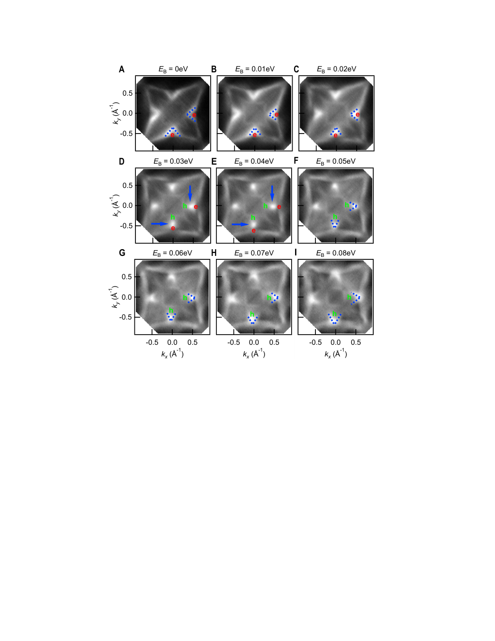
10.8.4 ARPES systematics on the blue Weyl line
We present an extended dataset for main text Fig. 1D-H (Fig. 10.15), with a finer sampling. We observe in greater detail the evolution of the dispersion from a to a dot to a . For instance, we find that the crossing point moves systematically away from with deeper , consistent with a line node. In ab initio, we observe a similar evolution for the blue Weyl line (Fig. 10.16A,B). We can better understand this evolution by considering the constant-energy surfaces for a generic line node (Fig. 10.16C,D). For above the line node, the slice intersects only the upper cone, giving I. For which cross the line node, we find electron and hole pockets intersecting at a point, as in II. As we continue to move downward the intersection point traces out the line node, shifting from left to right. Comparing to our ARPES spectra, we observe that the photoemission cross-section appears to be dominated by the intersection point for this range of . Lastly, as we scan below the line node, the intersection point completely zips closed the electron pocket and zips open the hole pocket, as in III. A detailed study of the dependence of the constant energy surface in ARPES again suggests a line node in Co2MnGa.

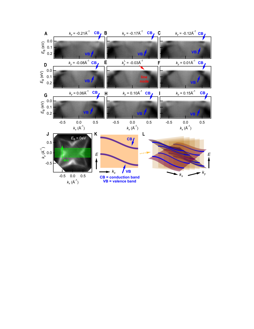
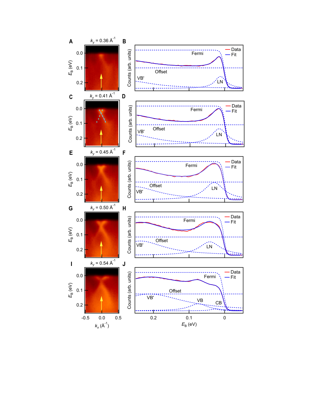
To provide another perspective, we cut parallel to the blue Weyl line (Fig. 10.17). In contrast to main text Figs. 1,2, here we cut along the Weyl line. Sweeping in , we see the conduction and valence bands approach (Fig. 10.17A-D), touch each other at fixed along a finite range of (Fig. 10.17E) and then move apart again (Fig. 10.17F-I). These parallel cuts again suggest a line node dispersion.
Next, we perform a Lorentzian peak fitting of the blue Weyl line. We begin with the cuts discussed in main text Fig. 2 and we choose the energy distribution curve (EDC) passing through the crossing point (Fig. 10.18). We fit these EDCs to the following form,
| (10.4) |
| (10.5) |
We include two Lorentzian peaks and , where the first peak corresponds to the line node crossing LN, while the second peak corresponds to a deeper valence band VB’ which is useful for improving the fit. We also include the Fermi-Dirac distribution and a constant offset which we interpret as a background spectral weight approximately constant within the energy range of the fit. We find a high-quality fit close to (Fig. 10.18A-D) using a single LN peak. Away from the crossing point, the peaks are well-described by a linear dispersion, further suggesting a band crossing (Fig. 10.18C). At , we observe that the fit begins to deviate from the data, and at there is an even more noticeable error (Fig. 10.18E-H). We speculate that this deviation may arise due to our finite resolution/linewidth as well as the fact that these spectra cut near the extremum of the Weyl line, producing a smeared-out energy gap. Another explanation considers the detailed dispersion of the blue Weyl line, which exhibits a rapid upward dispersion at its extremum (Fig. 10.14C). Due to broadening along , we may capture LN peaks from a range of , smearing out this rapid dispersion and producing a plateau structure in the EDC. For , we clearly observe two peaks on the EDC, so we fit with an additional Lorentzian (Fig. 10.18I-J). This gives VB and CB, the peaks corresponding to the conduction and valence bands of the line node. This interpretation is consistent with ab initio, which predicts that the blue Weyl line ends at .
Lastly, we take the results of our peak fitting and compare them with the calculated blue line node dispersion. We plot the LN peak maxima and the standard deviation of the peak positions, Fig. 10.19. We ignore EDCs at because the plateau shape in the EDC is poorly described by a single Lorentzian, as discussed above. We compare these numerical fitting results with a first-principles calculation of the blue Weyl line dispersion, shifted by eV. We find a reasonable quantitative agreement between the fit and calculated dispersion. Note that there is some expected contribution to the error from the ab initio calculation as well as corrections to the Lorentzian fitting form. These results support our observation of a line node in our ARPES spectra on Co2MnGa.


10.8.5 ARPES study of the yellow Weyl line
We can also observe signatures of yellow Weyl lines in our ARPES data, at incident photon energy . We can identify a candidate yellow Weyl line by comparing an ARPES constant-energy surface and the projected nodal lines (Fig. 10.20A, B). We reiterate that there are two different ways in which the yellow Weyl lines can project on the (001) surface. In particular, the four yellow Weyl lines along are “standing up”, so two crossings project onto the same point in the surface Brillouin zone, similar to the blue Weyl line we discussed above. By contrast, the outer yellow Weyl line runs in a single large loop around the entire surface Brillouin zone. It projects “lying down”, with single crossing projections. Here we focus on the double yellow line node. We study constant-energy surfaces at various binding energies (Fig. 10.20C-E) and we observe the same to switch that we discussed in the case of the blue Weyl line. We see similar behavior on an ab initio constant energy surface (Fig. 10.20I-K). Note crucially that the electron-to-hole transition occurs in the same direction in the ARPES spectra and calculation, suggesting that the line node dispersion has the same slope in experiment and theory. This provides additional evidence for the yellow Weyl line. Next we search for signatures of the yellow Weyl line on a series of cuts (green lines in Fig. 10.21G, H). We observe the upper cone near the center of the cut for closest to (Fig. 10.21A), corresponding to the yellow markers in Fig. 10.20C. As we slide away from , we observe the band crossing and lower cone (Fig. 10.21B, C). To pinpoint the cone, we study MDCs through the line node. We observe twin peaks corresponding to the upper and lower cone (10.21D,F), as well as a single peak when we cut through the line node (10.21E). In this way, we observe signatures of the “double” yellow Weyl line of Co2MnGa in our ARPES spectra.
Lastly, we search for signatures of the other, “single” yellow Weyl line. The outer features in Fig. 10.21B, C, as well as the large off-center peaks in Fig. 10.21E, F, correspond well to the predicted locations of the single yellow Weyl line. The valence band further shows a cone shape. However, we note that the conduction band appears to be shifted/offset in momentum relative to the valence band, for instance near the Fermi level at (Fig. 10.21B). This suggests that we are perhaps observing a surface state or surface resonance which partly traces out the line node. This explanation appears to be consistent with our calculations, compare main text Fig. 3E, which show a similar surface resonance. In summary, we provide evidence for the yellow Weyl lines in our ARPES spectra.

10.8.6 ARPES study of the red Weyl line
Having discussed the blue and yellow Weyl lines, we search for ARPES signatures of the red Weyl line. On the constant-energy surfaces, we observe a square feature around (Fig. 10.22F-H). This corresponds well to the predicted red Weyl line (Fig. 10.22D). Next, we study a series of cuts passing through the center square feature. We see two clear branches dispersing away from as we approach the Fermi level (red arrows, Fig. 10.22A-C). We can mark these features on an MDC (Fig. 10.22E). However, we observe no cone or crossing. We speculate that this may be because the other branch of the Weyl line has low photoemission cross-section under these measurement conditions.

10.8.7 Photon energy dependence of the drumhead surface state
We present an extended dataset to accompany main text Fig. 3, showing the drumhead surface states. In main text Fig. 3, we presented an energy distribution curve (EDC) stack cutting through the drumhead surface state at different photon energies. Here we present the full cut for each photon energy included in the stack. We observe the drumhead surface state consistently at all energies (orange arrow, Fig. 10.23A-I). Additionally, we show an EDC stack at a different momentum, , which cuts not through the drumhead surface state but the yellow line node cone (Fig. 10.23J) analogous to main text Fig. 3G. When cutting through the candidate drumhead, the EDC stack showed no dispersion in the peak energy as a function of photon energy, indicating no dispersion and suggesting a surface state. Here, by contrast, we can observe that the peak positions shift with photon energy (blue arrows). This shift suggests that the yellow line node lives in the bulk.
10.8.8 In-plane dispersion of the drumhead surface state
We briefly study the in-plane dispersion of the drumhead surface states. At eV, with Fermi surface as shown in Fig. 10.24A, we study a sequence of cuts scanning through the drumhead surface state, Fig. 10.24B-E. We observe that the surface state disperses slightly downward in energy as we scan away from and that it narrows in , as expected because the line node cones move towards each other as we approach the corner of the Brillouin zone. The dispersion of the candidate drumhead in-plane (but not out-of-plane) is consistent with the behavior of a surface state.

10.8.9 ARPES and ab initio study of the minority spin pocket
We briefly noted that Co2MnGa has a large minority spin pocket around the point (Fig. 10.12). We can omit this pocket from our ARPES measurements by an appropriate choice of photon energy , which then corresponds to a away from . In particular, at eV, main text Fig. 2, we find that we cut near the top of the Brillouin zone (near the point) and far from the point. As a result, we then compare our data with the majority spin bands from ab initio, as in main text Fig. 2E. However, to further compare ARPES and DFT, it is useful to search for this irrelevant pocket in ARPES and better understand why it does not compete with the line node and drumhead states in photoemission. In the DFT bulk projection, the minority spin projects onto a large pocket around , see Fig. 10.25A-C. Experimentally, we performed a photon energy dependence on a cut passing through . For eV we find that the red Weyl line disappears and a large hole pocket appears near (Fig. 10.26B-J). This pocket matches well with the minority spin pocket in calculation. This photon energy dependence suggests that the minority spin pocket does not interfere with our measurements of the Weyl lines because at eV we cut near the top of the bulk Brillouin zone in (near the point).


References
- [1] S.-Y. Xu et al., Hedgehog spin texture and Berry’s phase tuning in a magnetic topological insulator Nat. Phys. 8, 616 (2012).
- [2] D. Castelvecchi, The strange topology that is reshaping physics. Nature 547, 272 (2017).
- [3] S. R. Elliot, M. Franz, Colloquium: Majorana fermions in nuclear, particle, and solid-state physics. Rev. Mod. Phys. 87, 137 (2015).
- [4] Y. Tokura, M. Kawasaki, N. Nagaosa, Emergent functions of quantum materials. Nat. Phys. 13, 1056 (2017).
- [5] C.-Z. Chang, et al., Experimental observation of the quantum anomalous Hall effect in a magnetic topological insulator. Science 340, 167 (2013).
- [6] D. N. Basov, R. D. Averitt, D. Hsieh, Towards properties on demand in quantum materials. Nat. Mat. 16, 1077 (2017).
- [7] A. Bansil, H. Lin, T. Das, Topological band theory. Rev. Mod. Phys. 88, 021004 (2016).
- [8] M. Z. Hasan, C. L. Kane, Topological insulators. Rev. Mod. Phys. 82, 3045 (2010).
- [9] M. Z. Hasan, S.-Y. Xu, I. Belopolski, S.-M. Huang, Discovery of Weyl fermion semimetals and topological Fermi arc states. Ann. Rev. Cond. Matt. Phys. 2017, 289 (8).
- [10] N. P. Armitage, E. J. Mele, A. Vishwanath, Weyl and Dirac semimetals in three-dimensional solids. Rev. Mod. Phys. 90, 015001 (2018).
- [11] K. Manna, et al., From colossal to zero: Controlling the anomalous Hall effect in magnetic Heusler compounds via Berry curvature design (2017). arXiv:1712.10174.
- [12] A. Sakai, et al., Giant anomalous Nernst effect and quantum-critical scaling in a ferromagnetic semimetal. Nat. Phys. (2018). DOI:10.1038/s41567-018-0225-6.
- [13] E. Liu, et al., Giant anomalous Hall effect in a ferromagnetic kagome-lattice semimetal. Nat. Phys. (2018). DOI:10.1038/s41567-018-0234-5.
- [14] K. Kuroda, et al., Evidence for magnetic Weyl fermions in a correlated metal. Nat. Mat. 16, 1090 (2017).
- [15] K. Kim, et al., Large anomalous Hall current induced by topological nodal lines in a ferromagnetic van der Waals semimetal. Nat. Mat. (2018). DOI:10.1038/s41563-018-0132-3.
- [16] L. Ye, et al., Massive Dirac fermions in a ferromagnetic kagome metal. Nature 555, 638 (2018).
- [17] S. N. Guin, et al., Anomalous Nernst effect beyond the magnetization scaling relation in the ferromagnetic Heusler compound Co2MnGa (2018). arXiv:1806.06753.
- [18] H. Reichlova, et al., Large anomalous Nernst effect in thin films of the Weyl semimetal Co2MnGa (2018). arXiv:1807.06487.
- [19] G. Chang, et al., Topological Hopf and chain link semimetal states and their application to Co2MnGa. Phys. Rev. Lett. 119, 156401 (2017).
- [20] A. P. Schnyder, S. Ryu, A. Furusaki, A. W. Ludwig, Classification of topological insulators and superconductors in three spatial dimensions. Phys. Rev. B 78, 195125 (2008).
- [21] A. Vishwanath, A. M. Turner, Topological Insulators, Contemporary Concepts of Condensed Matter Science (Elsevier, 2013), Chap. 11.
- [22] C.-K. Chiu, A. P. Schnyder, Classification of reflection-symmetry-protected topological semimetals and nodal superconductors. Phys. Rev. B 90, 205136 (2014).
- [23] A. A. Burkov, M. D. Hook, L. Balents, Topological nodal semimetals. Phys. Rev. B 84, 235126 (2011).
- [24] R. Nandkishore, Weyl and Dirac loop superconductors. Phys. Rev. B 93, 020506 (2016).
- [25] Y. Wang, R. Nandkishore, Topological surface superconductivity in doped Weyl loop materials. Phys. Rev. B 95, 060506 (2017).
- [26] O. Stenull, C. L. Kane, T. C. Lubensky, Topological phonons and Weyl lines in three dimensions. Phys. Rev. Lett. 117, 068001 (2016).
- [27] G. Bian, et al., Topological nodal-line fermions in spin-orbit metal PbTaSe2. Nat. Commun. 7, 10556 (2016).
- [28] T. Bzdus̆ek, Q. Wu, A. Rüegg, M. Sigrist, A. A. Soluyanov, Nodal-chain metals. Nature 538, 75 (2016).
- [29] C.-K. Chiu, J. C. Y. Teo, A. P. Schnyder, S. Ryu, Classification of topological quantum matter with symmetries. Rev. Mod. Phys. 88, 035005 (2016).
- [30] Y. Kim, B. J. Wieder, C. L. Kane, A. M. Rappe, Dirac line nodes in inversion-symmetric crystals. Phys. Rev. Lett. 115, 036806 (2015).
- [31] Y.-H. Chan, C.-K. Chiu, M. Y. Chou, A. P. Schnyder, Ca3P2 and other topological semimetals with line nodes and drumhead surface states. Phys. Rev. B 93, 205132 (2016).
- [32] H. Ido, S. Yasuda, Magnetic properties of Co-Heusler and related mixed alloys. J. de Physique 49, C8 (1988).
- [33] Y. Tian, L. Ye, X. Jin, Proper scaling of the anomalous Hall effect. Phys. Rev. Lett. 103, 087206 (2009).
- [34] D. Hou, et al., Multivariable scaling for the anomalous Hall effect. Phys. Rev. Lett. 114, 217203 (2015).
- [35] L. Wu, K. Zhu, D. Yue, Y. Tian, X. Jin, Anomalous Hall effect in localization regime. Phys. Rev. B 93, 214418 (2016).
- [36] G. Bryant, Surface states of ternary semiconductor alloys: Effect of alloy fluctuations in one-dimensional models with realistic atoms. Phys. Rev. B 31, 5166 (1985).
- [37] T. Ozaki, http://www.openmx-square.org/.
- [38] G. Kresse, J. Furthmueller, Efficient iterative schemes for ab initio total-energy calculations using a plane-wave basis set. Phys. Rev. B 54, 11169 (1996).
- [39] G. Kresse, D. Joubert, From ultrasoft pseudopotentials to the projector augmented-wave method. Phys. Rev. B 59, 1758 (1999).
- [40] J. P. Perdew, K. Burke, M. Ernzerhof, Generalized gradient approximation made simple. Phys. Rev. Lett. 77, 3865 (1996).
- [41] E. V. Vidal, G. Stryganyuk, H. Schneider, C. Felser, G. Jakob, Exploring Co2MnAl Heusler compound for anomalous Hall effect sensors. App. Phys. Lett. 99, 132509 (2011).
- [42] N. Nagaosa, J. Sinova, S. Onoda, A. H. MacDonald, N. P. Ong, Anomalous Hall effect. Rev. of Mod. Phys. 82, 1539 (2010).
Appendix A Principal publications
- 1.
Ilya Belopolski et al. A three-dimensional magnetic topological phase. Submitted to Science (2018), arXiv:1712.09992.
- 2.
Daniel S. Sanchez*, Ilya Belopolski* et al. Topological chiral crystals with helicoid-arc quantum states. Nature 567, 500 (2019).
- 3.
Ilya Belopolski et al. A novel condensed matter lattice and a new platform for one-dimensional topological phases. Sci. Adv. 3, e1501692 (2017).
- 4.
Ilya Belopolski et al. Discovery of a new type of topological Weyl fermion semimetal state in MoxW1-xTe2. Nat. Commun. 7, 13643 (2016).
- 5.
Ilya Belopolski et al. Signatures of a time-reversal symmetric Weyl semimetal with only four Weyl points. Nat. Commun. 8, 942 (2017).
- 6.
M. Zahid Hasan, Su-Yang Xu, Ilya Belopolski and Shin-Ming Huang. Discovery of Weyl Fermion Semimetals and Topological Fermi Arc States. Ann. Rev. Cond. Mat. Phys. 8, 289 (2017).
- 7.
Su-Yang Xu*, Ilya Belopolski* et al. Discovery of a Weyl Fermion Semimetal and Topological Fermi Arcs. Science 349, 6248 (2015). [First Weyl semimetal: experiment]
- 8.
Shin-Ming Huang, Su-Yang Xu, Ilya Belopolski et al. A Weyl Fermion semimetal with surface Fermi arcs in the transition metal monopnictide TaAs class. Nat. Commun. 6, 7373 (2015). [First Weyl semimetal: prediction]
- 9.
Ilya Belopolski et al. Criteria for directly detecting topological Fermi arcs in Weyl semimetals. Phys. Rev. Lett. 116, 066802 (2016).
- 10.
Su-Yang Xu, Ilya Belopolski et al. Experimental discovery of a topological Weyl semimetal state in TaP. Sci. Adv. 1, e1501092 (2015).
- 11.
Su-Yang Xu, Nasser Alidoust, Ilya Belopolski et al. Discovery of a Weyl fermion state with Fermi arcs in niobium arsenide. Nat. Phys. 11, 748 (2015).
- 12.
Chenglong Zhang, Su-Yang Xu, Ilya Belopolski et al. Signatures of the Adler-Bell-Jackiw chiral anomaly in a Weyl Fermion semimetal. Nat. Commun. 7, 10735 (2016).
- 13.
Ilya Belopolski et al. Measuring Chern numbers above the Fermi level in the Type II Weyl semimetal MoxW1-xTe2. Phys. Rev. B 94, 085127 (2016).
- 14.
Su-Yang Xu, Ilya Belopolski et al. Spin polarization and texture of the Fermi arcs in the Weyl Fermion semimetal TaAs. Phys. Rev. Lett. 116, 096801 (2016).
Appendix B Complete list of publications
- 1.
Ilya Belopolski et al. A three-dimensional magnetic topological phase. Submitted to Science (2018), arXiv:1712.09992.
- 2.
Xitong Xu, Xirui Wang, Tyler A. Cochran, Daniel S. Sanchez, Ilya Belopolski et al. Crystal growth and quantum oscillations in the topological chiral semimetal CoSi. arXiv:1904.00630.
- 3.
Jia-Xin Yin, Songtian S. Zhang, Guoqing Chang, Qi Wang, Stepan Tsirkin, Zurab Guguchia, Biao Lian, Huibin Zhou, Kun Jiang, Ilya Belopolski et al. Negative flat band magnetism in a spin-orbit coupled correlated kagome magnet. Nat. Phys. (2019).
- 4.
Daniel S. Sanchez*, Ilya Belopolski* et al. Topological chiral crystals with helicoid-arc quantum states. Nature 567, 500 (2019).
- 5.
Guoqing Chang, Benjamin J. Wieder, Frank Schindler, Daniel S. Sanchez, Ilya Belopolski et al. Topological quantum properties of chiral crystals. Nat. Mat. (2018).
- 6.
Jia-Xin Yin, Songtian S. Zhang, Hang Li, Kun Jiang, Guoqing Chang, Bingjing Zhang, Biao Lian, Cheng Xiang, Ilya Belopolski et al. Giant and anisotropic many-body spin-orbit tunability in a strongly correlated kagome magnet. Nature 562, 91-95 (2018).
- 7.
Jiaxin Yin, Songtian S. Zhang, Guangyang Dai, Hao Zheng, Guoqing Chang, Ilya Belopolski et al. Vector field based emergent phase diagram in a correlated superconductor. arXiv:1802.10059.
- 8.
M. Mofazzel Hosen, Klauss Dimitri, Alex Aperis, Pablo Maldonado, Ilya Belopolski et al. Observation of Gapless Dirac Surface States in ZrGeTe. Phys. Rev. B 97, 121103 (2018).
- 9.
Hao Zheng, Guoqing Chang, Shin-Ming Huang, Cheng Guo, Xiao Zhang, Songtian Zhang, Jiaxin Yin, Su-Yang Xu, Ilya Belopolski et al. Mirror protected Dirac fermions on a Weyl semimetal NbP surface. Phys. Rev. Lett. 119, 196403 (2017).
- 10.
Guoqing Chang, Su-Yang Xu, Xiaoting Zhou, Shin-Ming Huang, Bahadur Singh, Baokai Wang, Ilya Belopolski et al. Topological Hopf and chain link semimetal states and their application to Co2MnGa. Phys. Rev. Lett. 119, 156401 (2017).
- 11.
Guoqing Chang, Su-Yang Xu, Benjamin J. Wieder, Daniel S. Sanchez, Shin-Ming Huang, Ilya Belopolski et al. Large Fermi Arcs in Unconventional Weyl Semimetal RhSi. Phys. Rev. Lett. 119, 206401 (2017).
- 12.
Q. R. Zhang, B. Zeng, D. Rhodes, S. Memaran, T. Besara, R. Sankar, F. Chou, N. Alidoust, S.-Y. Xu, Ilya Belopolski et al. Magnetic field-induced electronic and topological phase transitions in Weyl type-I semi-metals. arXiv:1705.00920
- 13.
Ilya Belopolski et al. A novel condensed matter lattice and a new platform for one-dimensional topological phases. Sci. Adv. 3, e1501692 (2017).
- 14.
M. Zahid Hasan, Su-Yang Xu, Ilya Belopolski and Shin-Ming Huang. Discovery of Weyl Fermion Semimetals and Topological Fermi Arc States. Ann. Rev. Cond. Mat. Phys. 8, 289 (2017).
- 15.
Ilya Belopolski et al. Topological Weyl phase transition in MoxW1-xTe2. arXiv:1612.07793
- 16.
M. Mofazzel Hosen, Klauss Dimitri, Ilya Belopolski et al. Tunability of the topological nodal-line semimetal phase in ZrSi-type materials ( S, Se, Te). Phys. Rev. B. 95, 161101 (2017).
- 17.
Ilya Belopolski, et al. Discovery of a new type of topological Weyl fermion semimetal state in MoxW1-xTe2. Nat. Commun. 7, 13643 (2016).
- 18.
Hao Zheng, Guang Bian, Guoqing Chang, Hong Lu, Su-Yang Xu, Guangqiang Wang, Tay-Rong Chang, Songtian Zhang, Ilya Belopolski, et al. Atomic-Scale Visualization of Quasiparticle Interference on a Type-II Weyl Semimetal Surface. Phys. Rev. Lett. 117, 266804 (2016).
- 19.
Guoqing Chang, Daniel S. Sanchez, Benjamin J. Wieder, Su-Yang Xu, Frank Schindler, Ilya Belopolski, et al. Kramers theorem-enforced Weyl fermions: Theory and Materials Predictions (Ag3BO3, TlTe2O6 and Ag2Se related families). arXiv:1611.07925
- 20.
Madhab Neupane, Nasser Alidoust, M. Mofazzel Hosen, Jian-Xin Zhu, Klauss Dimitri, Su-Yang Xu, Nagendra Dhakal, Raman Sankar, Ilya Belopolski, et al. Observation of the spin-polarized surface state in a noncentrosymmetric superconductor BiPd. Nat. Commun. 7, 13315 (2016).
- 21.
Ilya Belopolski, et al. A minimal, “hydrogen atom” version of an inversion-breaking Weyl semimetal. Nat. Commun. (2017) & arXiv:1610.02013
- 22.
Tay-Rong Chang, Su-Yang Xu, Daniel S. Sanchez, Shin-Ming Huang, Guoqing Chang, Chuang-Han Hsu, Guang Bian, Ilya Belopolski, et al. Type-II Topological Dirac Semimetals: Theory and Materials Prediction (VAl3 family). arXiv:1606.07555
- 23.
Guoqing Chang, Su-Yang Xu, Shin-Ming Huang, Daniel S. Sanchez, Chuang-Han Hsu, Guang Bian, Zhi-Ming Yu, Ilya Belopolski, et al. Nexus fermions in topological symmorphic crystalline metals. Sci. Rep. 7, 1688 (2017).
- 24.
Madhab Neupane, M Mofazzel Hosen, Ilya Belopolski, et al. Observation of Dirac-like semi-metallic phase in NdSb. J. Phys: Cond. Mat. 28, 23LT02 (2016).
- 25.
Su-Yang Xu, Nasser Alidoust, Guoqing Chang, Hong Lu, Bahadur Singh, Ilya Belopolski, et al. Discovery of Lorentz-violating Weyl fermion semimetal state in LaAlGe materials. arXiv:1603.07318.
- 26.
Ilya Belopolski, et al. Criteria for directly detecting topological Fermi arcs in Weyl semimetals. Phys. Rev. Lett. 116, 066802 (2016).
- 27.
Chenglong Zhang, Su-Yang Xu, Ilya Belopolski, et al. Signatures of the Adler-Bell-Jackiw chiral anomaly in a Weyl Fermion semimetal. Nat. Commun. 7, 10735 (2016).
- 28.
Nasser Alidoust, A. Alexandradinata, Su-Yang Xu, Ilya Belopolski, et al. A new form of (unexpected) Dirac fermions in the strongly-correlated cerium monopnictides. arXiv: 1604.08571
- 29.
Ilya Belopolski, et al. Measuring Chern numbers above the Fermi level in the Type II Weyl semimetal MoxW1-xTe2. Phys. Rev. B. 94, 085127 (2016).
- 30.
Guoqing Chang, Bahadur Singh, Su-Yang Xu, Guang Bian, Shin-Ming Huang, Chuang-Han Hsu, Ilya Belopolski, et al. Theoretical prediction of magnetic and noncentrosymmetric Weyl fermion semimetal states in the -Al- family of compounds ( rare earth, Al aluminium, Si, Ge). arXiv:1604.02124
- 31.
Madhab Neupane, Ilya Belopolski, et al. Observation of topological nodal fermion semimetal phase in ZrSiS. Phys. Rev. B. 93, 201104 (2016).
- 32.
Su-Yang Xu, Nasser Alidoust, Guoqing Chang, Hong Lu, Bahadur Singh, Ilya Belopolski, et al. Discovery of Lorentz-violating type II Weyl fermions in LaAlGe. Sci. Adv. 3, e1603266 (2017).
- 33.
Guoqing Chang, Su-Yang Xu, Hao Zheng, Bahadur Singh, Chuang-Han Hsu, Guang Bian, Nasser Alidoust, Ilya Belopolski, et al. Room-temperature magnetic topological Weyl fermion and nodal line semimetal states in half-metallic Heusler Co2Ti ( Si, Ge, or Sn). Sci. Rep. 6, 38839 (2016).
- 34.
Cheng-Long Zhang, Su-Yang Xu, Ilya Belopolski, et al. Signatures of the Adler-Bell-Jackiw chiral anomaly in a Weyl fermion semimetal. Nat. Commun. 7, 10735 (2016).
- 35.
Guoqing Chang, Su-Yang Xu, Daniel S. Sanchez, Shin-Ming Huang, Chi-Cheng Lee, Tay-Rong Chang, Hao Zheng, Guang Bian, Ilya Belopolski, et al. A strongly robust Weyl fermion semimetal state in Ta3S2. Sci. Adv. 2, e1600295 (2016).
- 36.
Tay-Rong Chang, Peng-Jen Chen, Guang Bian, Titus Neupert, Raman Sankar, Su-Yang Xu, Ilya Belopolski, et al. Topological Dirac States and Pairing Correlations in the Non-Centrosymmetric Superconductor PbTaSe2. Phys. Rev. B. 93, 245130 (2016)
- 37.
Guoqing Chang, Su-Yang Xu, Hao Zheng, Chi-Cheng Lee, Shin-Ming Huang, Ilya Belopolski, et al. Quasi-particle interferences of the Weyl semimetals TaAs and NbP. Phys. Rev. Lett. 116, 066601 (2016).
- 38.
Guang Bian, Ting-Fung Chung, Chang Liu, Chaoyu Chen, Tay-Rong Chang, Tailung Wu, Ilya Belopolski, et al. Experimental observation of two massless Dirac fermion gases in graphene-topological insulator heterostructure. 2D Mat. 3, 021009 (2016).
- 39.
Hao Zheng, Su-Yang Xu, Guang Bian, Cheng Guo, Guoqing Chang, Daniel S. Sanchez, Ilya Belopolski, et al. Atomic Scale Visualization of Quantum Interference on a Weyl Semimetal Surface by Scanning Tunneling Microscopy/Spectroscopy. ACS Nano 10, 1378 (2016).
- 40.
Madhab Neupane, Yukiaki Ishida, Raman Sankar, Jian-Xin Zhu, Daniel S. Sanchez, Ilya Belopolski, et al. Electronic structure and relaxation dynamics in a superconducting topological material. Sci. Rep. 6, 22557 (2016).
- 41.
Su-Yang Xu, Ilya Belopolski, et al. Spin polarization and texture of the Fermi arcs in the Weyl Fermion semimetal TaAs. Phys. Rev. Lett. 116, 096801 (2016).
- 42.
Guang Bian, Tay-Rong Chang, Hao Zheng, Saavanth Velury, Su-Yang Xu, Titus Neupert, Ching-Kai Chiu, Daniel S. Sanchez, Ilya Belopolski, et al. Drumhead Surface States and Topological Nodal-Line Fermions in TlTaSe2. Accepted in Phys. Rev. B. (2016).
- 43.
Tay-Rong Chang, Su-Yang Xu, Guoqing Chang, Chi-Cheng Lee, Shin-Ming Huang, BaoKai Wang, Guang Bian, Hao Zheng, Daniel S. Sanchez, Ilya Belopolski, et al. Prediction of an arc-tunable Weyl fermion metallic state in MoxW1-xTe2. Nat. Commun. 7, 10639 (2016).
- 44.
Madhab Neupane, Su-Yang Xu, Yukiaki Ishida, Shuang Jia, Benjamin M. Fregoso, Chang Liu, Ilya Belopolski, et al. Gigantic surface life-time of an intrinsic topological insulator revealed via time-resolved (pump-probe) ARPES. Phys. Rev. Lett. 115, 116801 (2015).
- 45.
Chi-Cheng Lee, Su-Yang Xu, Shin-Ming Huang, Daniel S. Sanchez, Ilya Belopolski, et al. Fermi arc topology and interconnectivity in Weyl fermion semimetals TaAs, TaP, NbAs and NbP. Phys. Rev. B 92, 235104 (2015).
- 46.
Madhab Neupane, Su-Yang Xu, R. Sankar, Q. Gibson, Y. J. Wang, Ilya Belopolski, et al. Topological phase diagram and saddle point singularity in a tunable topological crystalline insulator. Phys. Rev. B 92, 075131 (2015).
- 47.
Su-Yang Xu, Ilya Belopolski, et al. Experimental discovery of a topological Weyl semimetal state in TaP. Sci. Adv. 1, e1501092 (2015).
- 48.
Madhab Neupane, Nasser Alidoust, Su-Yang Xu, Ilya Belopolski, et al. Discovery of the topological surface state in a noncentrosymmetric superconductor BiPd. arXiv:1505.03466.
- 49.
Guang Bian, Tay-Rong Chang, Raman Sankar, Su-Yang Xu, Hao Zheng, Titus Neupert, Ching-Kai Chiu, Shin-Ming Huang, Guoqing Chang, Ilya Belopolski, et al. Topological nodal-line fermions in spin-orbit metal PbTaSe2. Nat. Commun. 7, 10556 (2016).
- 50.
Su-Yang Xu, Nasser Alidoust, Ilya Belopolski, et al. Discovery of a Weyl fermion state with Fermi arcs in niobium arsenide. Nat. Phys. 11, 748 (2015).
- 51.
Su-Yang Xu, Madhab Neupane, Ilya Belopolski, et al. Unconventional transformation of spin Dirac phase across a topological quantum phase transition. Nat. Commun. 6, 6870 (2015).
- 52.
Shin-Ming Huang, Su-Yang Xu, Ilya Belopolski, et al. New type of Weyl semimetal with quadratic double Weyl fermions. PNAS 5, 113 (2016).
- 53.
Su-Yang Xu, Chang Liu, Ilya Belopolski, et al. Lifshitz transition and van Hove singularity in a Topological Dirac Semimetal. Phys. Rev. B 92, 075115 (2015).
- 54.
Su-Yang Xu*, Ilya Belopolski*, et al. Discovery of a Weyl Fermion Semimetal and Topological Fermi Arcs. Science 349, 6248 (2015).
- 55.
Satya K. Kushwaha, Jason W. Krizan, Benjamin E. Feldman, Andras Gyenis, Mallika T. Randeria, Jun Xiong, Su-Yang Xu, Nasser Alidoust, Ilya Belopolski, et al. Bulk crystal growth and electronic characterization of the 3D Dirac Semimetal Na3Bi. APL Mater. 3, 041504 (2015).
- 56.
Su-Yang Xu, Chang Liu, Satya K. Kushwaha, Raman Sankar, Jason W. Krizan, Ilya Belopolski, et al. Observation of Fermi arc surface states in a topological metal. Science 347, 6219 (2015).
- 57.
Shin-Ming Huang, Su-Yang Xu, Ilya Belopolski, et al. A Weyl Fermion semimetal with surface Fermi arcs in the transition metal monopnictide TaAs class. Nat. Commun. 6, 7373 (2015).
- 58.
Madhab Neupane, Su-Yang Xu, Nasser Alidoust, Raman Sankar, Ilya Belopolski, et al. Surface Versus Bulk Dirac States Tuning in a Three-Dimensional Topological Dirac Semimetal. Phys. Rev. B 91, 241114 (2015).
- 59.
Madhab Neupane, Nasser Alidoust, Guang Bian, Su-Yang Xu, Ilya Belopolski, et al. Fermi Surface Topology and Hotspots Distribution in Kondo Lattice System CeB6. Phys. Rev. B 92, 104420 (2015).
- 60.
Nasser Alidoust, Chang Liu, Su-Yang Xu, Ilya Belopolski, et al. Observation of metallic surface states in the strongly correlated Kitaev-Heisenberg candidate Na2IrO3. arXiv:1410.6389.
- 61.
Su-Yang Xu, Nasser Alidoust, Ilya Belopolski, et al. Momentum-space imaging of Cooper pairing in a half-Dirac-gas topological superconductor. Nat. Phys. 10, 943 (2014).
- 62.
Madhab Neupane, Su-Yang Xu, Nasser Alidoust, Guang Bian, Dae-Jeong Kim, Chang Liu, Ilya Belopolski, et al. Non-Kondo-like Electronic Structure in the Correlated Rare-Earth Hexaboride YbB6. Phys. Rev. Lett. 114, 016403 (2015).
- 63.
Madhab Neupane, Anthony Richardella, Jaime Sanchez-Barriga, Su-Yang Xu, Nasser Alidoust, Ilya Belopolski, et al. Observation of quantum-tunneling modulated spin texture in ultrathin topological insulator Bi2Se3 films. Nat. Commun. 5, 3841 (2014).
- 64.
Chang Liu, Su-Yang Xu, Nasser Alidoust, Tay-Rong Chang, Hsin Lin, Chetan Dhital, Sovit Khadka, Madhab Neupane, Ilya Belopolski, et al. Spin-correlated electronic state on the surface of a spin-orbit Mott system. Phys. Rev. B 90, 045127 (2014).
- 65.
Su-Yang Xu, Chang Liu, Anthony Richardella, Ilya Belopolski, et al. Fermi-level electronic structure of a topological-insulator/cuprate-superconductor in the superconducting proximity effect regime. Phys. Rev. B 90, 085128 (2014).
- 66.
Nasser Alidoust, Guang Bian, Su-Yang Xu, Raman Sankar, Madhab Neupane, Chang Liu, Ilya Belopolski, et al. Observation of monolayer valence band spin-orbit effect and induced quantum well states in Mo. Nat. Commun. 5, 4673 (2014).
- 67.
Su-Yang Xu, Chang Liu, S. K. Kushwaha, T.-R. Chang, J. W. Krizan, R. Sankar, C. M. Polley, J. Adell, T. Balasubramanian, K. Miyamoto, N. Alidoust, Guang Bian, M. Neupane, Ilya Belopolski, et al. Observation of a bulk 3D Dirac multiplet, Lifshitz transition, and nestled spin states in Na3Bi. arXiv:1312.7624.
- 68.
Madhab Neupane, Nasser Alidoust, SuYang Xu, Takeshi Kondo, Yukiaki Ishida, Dae-Jeong Kim, Chang Liu, Ilya Belopolski, et al. Surface electronic structure of the topological Kondo insulator candidate correlated electron system SmB6. Nat. Commun. 4, 2991 (2013).
- 69.
M. Neupane, N. Alidoust, Suyang Xu, Chang Liu, Ilya Belopolski, et al. An experimental algorithm for identifying the topological nature of Kondo and mixed valence insulators. arXiv:1311.7111.
- 70.
Madhab Neupane, Su-Yang Xu, R. Sankar, N. Alidoust, G. Bian, Chang Liu, Ilya Belopolski, et al. Observation of a three-dimensional topological Dirac semimetal phase in high-mobility Cd3As2. Nat. Commun. 5, 3786 (2014).
- 71.
M. Neupane, S. Basak, N. Alidoust, S.-Y. Xu, Chang Liu, Ilya Belopolski, et al. Oscillatory surface dichroism of an insulating topological insulator Bi2Te2Se. Phys. Rev. B. 88, 165129 (2013).
- 72.
Su-Yang Xu, Chang Liu, Nasser Alidoust, M. Neupane, D. Qian, Ilya Belopolski, et al. Observation of a topological crystalline insulator phase and topological phase transition in Pb1-xSnxTe. Nat. Commun. 3, 1192 (2012).