Plasmon-enhanced graphene photodetector with CMOS-compatible titanium nitride
Abstract
Graphene has emerged as an ultrafast optoelectronic material for on-chip photodetector applications. The 2D nature of graphene enables its facile integration with complementary metal-oxide semiconductor (CMOS) microelectronics and silicon photonics, yet graphene absorbs only 2.3% of light. Plasmonic metals can enhance the responsivity of graphene photodetectors, but may result in CMOS-incompatible devices, depending on the choice of metal. Here, we propose a plasmon-enhanced photothermoelectric graphene detector using CMOS-compatible titanium nitride (TiN) on the silicon-on-insulator (SOI) platform. The device performance is quantified by its responsivity, operation speed, and noise equivalent power. Its bandwidth exceeds 100 GHz, and it exhibits a nearly flat photoresponse across the telecom C-band. The photodetector responsivity is as high as 1.4 A/W (1.1 A/W external) at an ultra-compact length of 3.5 µm, which is the most compact footprint reported for a graphene-based waveguide photodetector. Furthermore, it operates at zero-bias, consumes zero energy, and has an ultra-low intrinsic noise equivalent power (NEP <).
keywords
American Chemical Society, LaTeX1 Introduction
The integration of optical interconnects with CMOS microelectronics for ultra-high-speed links has become an industrial necessity Sousa and Achard 2016. Unlike lossy metallic links, integrated optical interconnects can sustain the transmission of ultrafast signals with losses as low as 0.1 dB/cm using the silicon-on-insulator (SOI) platform Chen et al. 2018. Moreover, silicon photonics and CMOS microelectronics are both based on silicon, and can in principle function hand-in-hand within a single chip. However, the size disparity between diffraction-limited photonics and advanced CMOS technology nodes, in addition to fabrication and co-integration challenges impede this progress. Introducing plasmonic metals to photonic devices to excite surface plasmon polaritons (SPPs), is one viable solution to this problem, at least for some functionalities, such as photodetection. SPPs are electromagnetic (EM) excitations that exist at the interface between a metal and a dielectric (or a semiconductor). These unique EM excitations result in a significant enhancement of the EM field at the metal-dielectric interface, where light can also be confined beyond its diffraction limit Zhang et al. 2012.
Optical interconnects consist of a transmitter, waveguide, and a receiver. The receiver contains a photodetector that converts optical signals to electrical ones. A photodetector is differentiated by its responsivity, speed, footprint, dark current, energy consumption, and ease of integration with standard industrial platforms. Most photodetectors employed in silicon photonics are based on Germanium Akinwande et al. 2019. However, these photodetectors are either resistance-capacitance (RC) product or carrier transit-time limited. Incorporating plasmonic waveguides and applying a large bias voltage can push the speed of Germanium photodetectors up to 110 GHz Salamin et al. 2018, however high energy consumption and large dark currents are associated with this boost. Plasmonic Schottky photodetectors have been proposed for their ease of integration with silicon photonics, and their ability to absorb photons at telecom wavelengths, with a demonstrated responsivity of 0.37 A/W at 3 V bias Goykhman et al. 2016. Nonetheless, huge dark currents are associated with plasmonic Schottky photodetectors, which could hinder their implementation in applications where high signal-to-noise (SNR) ratios are essential, e.g. telecom. III-V compound semiconductors, that are heterogeneously integrated on silicon, can exhibit a decent performance in terms of speed and responsivity Sun and Beling 2019, yet their performance is degraded when integrated with CMOS microelectronics due to packaging parasitics. Besides that, heterogeneous integration techniques are expensive Koester et al. 2006; Klamkin et al. 2018. Furthermore, the monolithic integration of III-V compound semiconductors with silicon is hindered by the the large mismatches in their lattice constants and thermal expansion coefficients Jung et al. 2016.
Two-dimensional (2D) materials recently emerged as alternative active materials for modulation and photodetection with a special set of inherent features including high-speed, small footprint, low-cost manufacturing, low-power consumption, and CMOS-compatibility Akinwande et al. 2019. More specifically, graphene photodetectors gained extraordinary attention for their ultrafast speed and broadband absorption, despite the innate, relatively low optical absorption of graphene Xia et al. 2009; Koppens et al. 2014; Gan et al. 2013; Wang et al. 2013; Xie et al. 2018; Di Bartolomeo et al. 2018; Youngblood et al. 2014; Wang et al. 2015. Several techniques were proposed to boost the responsivity of high-speed graphene photodetectors including waveguide-integrated configurations where light continuously interacts with the graphene sheet as it propagates through the waveguide, combining graphene with other 2D materials in composite heterostructures, and enhancing graphene’s absorption by plasmonic means. So far, the demonstrated waveguide-integrated plasmonic graphene photodetectors are all based on gold Ma et al. 2019; Guo et al. 2020; Muench et al. 2019; Ding et al. 2019, which in spite of its outstanding plasmonic performance, is not CMOS-compatible Lefebvre et al. 2016.
In this work, we propose an on-chip, compact footprint, ultrafast and high responsivity plasmon-enhanced graphene photodetector that operates at the telecom C-band, and which can be realized using CMOS-compatible processes. The proposed device employs titanium nitride (TiN) as the plasmonic material. TiN is a refractory metal nitride that has optical properties very similar to gold Catellani and Calzolari 2017, an electrical conductivity higher than Titanium TiN 1996, yet unlike gold, TiN is CMOS-compatible Patsalas et al. 2015; Gosciniak et al. 2019; Briggs et al. 2016. The device performance is studied and quantified in terms of its responsivity, operation speed, energy consumption, and noise equivalent power.
2 Device Structure
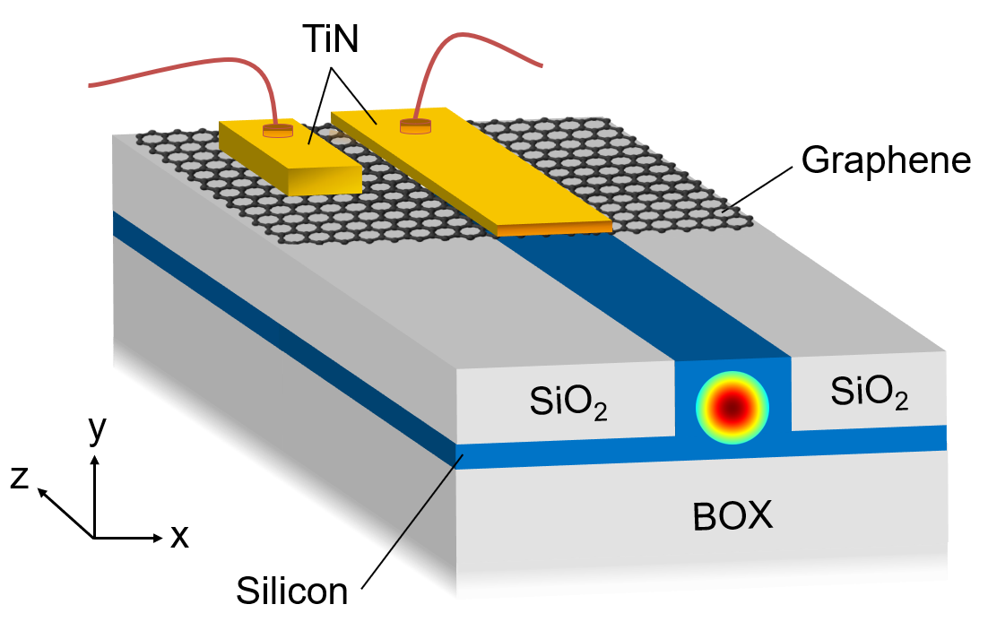
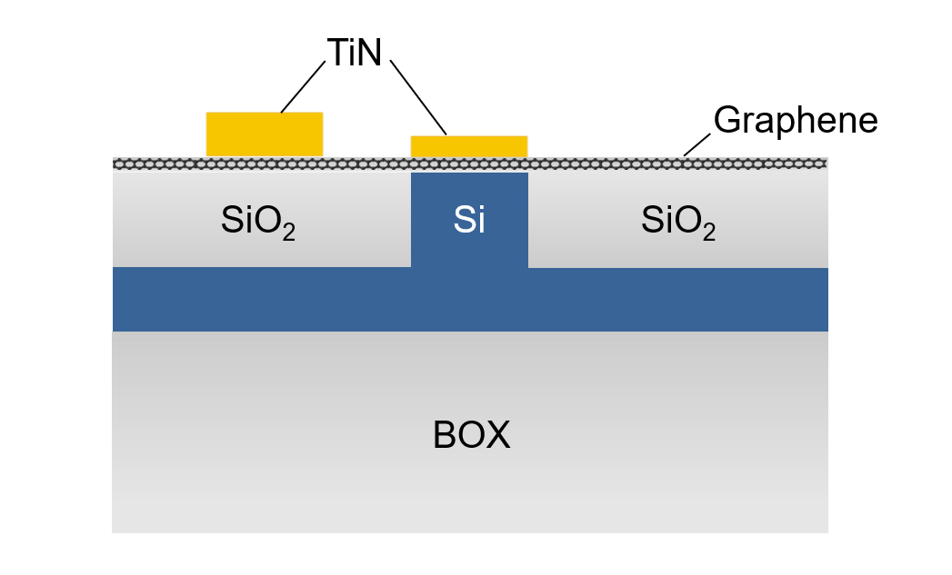
The structure of the on-chip photodetector is illustrated in Fig 1. A silicon rib waveguide on top of a 2 µm bottom oxide (BOX) layer guides the incoming light to the photodetector section at the terminating end of the optical link, where the optical signal is absorbed and reverted to its electrical form. The waveguide supports a transverse magnetic (TM)-mode. Within the photodetector section, silicon dioxide (SiO2) is deposited on the sides of the waveguide ridge to facilitate the placement of the graphene monolayer on top of the waveguide. The generated electrical signal is collected through the two TiN films that are deposited on top of graphene. Besides collecting the signal, the center TiN film plasmonically enhances the interaction of the propagating TM-mode with graphene, which boosts the optical absorption of the latter, resulting in a high photoresponse at an ultra-compact device length of 3.5 µm. Details of the device geometry, optimization procedure, propagation modes, plasmon-induced losses, and the impact of potential fabrication variations are provided in supplementary section 1.
3 Operation Principle
Graphene detects light mainly through three physical effects: the photovoltaic Peters et al. 2010; Rao et al. 2011; Mueller et al. 2009, bolometric Jago et al. 2019; Wang et al. 2016; Vora et al. 2012, and photo-thermoelectric (PTE) Cai et al. 2014; Basko 2011; Xu et al. 2009 effects. The bolometric effect is only observed for devices under bias Freitag et al. 2012, which is not the case for our device. The PTE effect dominates over the photovoltaic effect at zero bias Song et al. 2011; thus, the photodetection process in our device is predominantly determined by the PTE effect. This effect is based on the phenomenon of photogenerated hot carriers in graphene. Due to the unique conical dispersion of graphene, the density of states fades away at the Dirac point. As a consequence, carriers have a low heat capacity near the Dirac point, and when excited, they immediately scatter with other carriers within a few tens of femtoseconds. These carrier-carrier scattering events result in an ephemeral Fermi-Dirac distribution of hot thermalized carriers, which can be described by a chemical potential (µ) and a carrier temperature (Tc) Chen et al. 2019. Afterwards, the hot thermalized carriers cool down in picoseconds by emitting optical and acoustic phonons, coupling with surface optical phonons, and most importantly through disorder-assisted scattering which dominates at room temperature Song et al. 2012; Ma et al. 2014; Chen et al. 2008.


Within the photodetector section, the propagating TM-mode experiences a near-field plasmonic enhancement at the TiN-graphene-Si interface due to the presence of the TiN stripe. This near-field enhancement results in a plasmon-enhanced effective absorption of graphene, and hot carriers are generated as the propagating mode interacts with the graphene sheet. An uneven distribution of hot carriers across the graphene sheet induces a PTE voltage Shautsova et al. 2018; gra 2018:
| (1) |
The Seebeck coefficient is a function of the chemical potential, and resembles the curve shown in Fig 2(a). According to Eq. (1), an asymmetric profile of the Seebeck coefficient across the graphene sheet induces a PTE voltage. Graphene is effectively doped when placed in contact with a metal, which in turn affects the Seebeck coefficient and the PTE voltage. The resulting shift in chemical potential (µ) is related to the Shottky barrier height ( at the metal-graphene junction, which is approximated using the Schottky-Mott rule Pierret 1996; Mönch 2017:
| (2) |
Where is the metal work function, and is the electron affinity of the semiconductor given by:
| (3) |
Where is the work function, is the energy of the conduction band edge, and is the Fermi energy of the semiconductor. Here we consider TiN, a metal nitride, as the metal, and graphene, a zero-bandgap semiconductor, as the semiconductor. Considering the case of an ideally undoped graphene, gives and . Taking work function values of eV for graphene Yu et al. 2009; Naghdi et al. 2019, and 4.2 –eV for TiN Lima et al. 2012; Fillot et al. 2005, gives , leading to electrons flowing from graphene to TiN, or graphene being effectively p-doped by TiN, and the Seebeck coefficient varies as a result (see Fig 2(b)). For this device however, the Seebeck coefficient does not contribute to the generated photovoltage, since TiN is placed on both sides of the graphene sheet, giving a symmetric doping profile across it. A difference in the Seebeck coefficient across the graphene sheet is required to generate a for a fixed profile based on Song et al. 2011:
| (4) |
Where and represent the Seebeck coefficient at each side of the graphene sheet, and is the lattice temperature. Therefore, the photodetector operates solely based on the plasmonic thermoelectric effect. The previous analysis assumes an ideal metal-semiconductor interface. In practice, is experimentally extracted as described in Pierret 1996, since the Schottky-Mott rule does not take into account the presence of charged impurities at the metal-semiconductor interface. Even so, a similar conclusion can be reached because of the symmetric doping profile induced by the TiN-graphene-TiN configuration.
The carrier temperature profile across the graphene sheet is given by solving the heat transport equation Song et al. 2011; Shiue et al. 2015; Lin et al. 2019:
| (5) |
Where is the carrier cooling rate, is the carrier heat capacity, the effective optical absorption of graphene (see Methods), and is the intensity profile of the excitation waveguide mode (see section 4 of the supporting information). The product of the carrier temperature profile and the Seebeck coefficient is later integrated to find out the induced PTE voltage, according to Eq. 1. Finally, the voltage responsivity of the photodetector is calculated by dividing the PTE voltage by the total input optical power in the waveguide. In this work, we plug in parameters taken from experimental reports to the heat transport equation. First, the electrical conductivity () of graphene is calculated as Song et al. 2011; Lin et al. 2019; Shiue et al. 2015:
| (6) |
Where is the minimum conductivity taken from Lin et al. 2019, is Planck’s constant, and is the minimum conductivity plateau; meV for graphene-on-SiO2 Lin et al. 2019; Dorgan et al. 2010. The thermal conductivity () is related to the electrical conductivity () through the Wiedemann-Franz Law:
| (7) |
The carrier cooling rate () can be expressed as Ma et al. 2014; Lin et al. 2019:
| (8) |
| (9) |
| (10) |
The first term in the right hand side of Eq. (8) is related to intrinsic scattering processes that dominate at low temperatures, while the second term is related to disorder-assisted scattering which dominates at high temperatures, including room temperature (). is the electron-phonon coupling constant, is the density of states, is the mean free path, is the Fermi wave vector, is the Bloch-Grüneisen temperature, 20 eV is the deformation potential constant Song et al. 2012, Kg/m2 is the mass density of graphene, and m/s is the speed of longitudinal acoustic phonons gra 2018. The carrier heat capacity () is given by Phillips and Fisher 2005:
| (11) |
The carrier cooling length () is related to , , and by the following relation:
| (12) |
Now we have the ingredients required for solving the heat transport equation. The carrier temperature profile is calculated using the analytical solution to the heat transport equation Ma et al. 2014; Gosciniak et al. 2020:
| (13) |
Where is the distance from the peak of to the side electrode. The carrier temperature is multiplied by the Seebeck coefficient, which is given by the Mott Formula:
| (14) |
The photocurrent is calculated by dividing the resultant PTE voltage by the resistance of the graphene sheet ():
| (15) |
Where is the electrodes spacing, and is the photodetector length. Finally, the current responsivity is calculated by dividing the photocurrent by the total input optical power in the waveguide.
4 Methods
The optimization procedure, presented in supplementary section 1, was carried out for the graphene-on-SiO2 waveguide photodetector. The refractive index of TiN was taken as at nm Gosciniak et al. 2019; Gosciniak et al. 2016 (see supplementary section 3). Simulations were conducted using Lumerical, where graphene is modeled as a 2D material with a surface optical conductivity () given by Lumerical; Falkovsky 2008:
| (16) |
| (17) |
| (18) |
| (19) |


and account for the surface optical conductivity due to intraband and interband transitions, respectively. is the angular frequency of incident photons, is the scattering rate of graphene, is the operation temperature, is the electron charge, is the reduced Planck constant, is the Fermi-Dirac distribution, and is the Boltzmann constant. The surface electric permittivity () and the surface electric susceptibility () are related to through the following relation gra 2018:
| (20) |
In general, graphene samples are unintentionally doped when placed on a substrate, which results in a chemical potential in the range of 0.1– 0.2 eV Ooi et al. 2017; Romero et al. 2008. In this work, we model graphene with a 0.15 eV chemical potential and 1 ps scattering time. The scattering time is related to the scattering rate by . An incident photon has a 0.8 eV energy at nm; this photon induces an interband transition when absorbed by graphene since 2µ (see supplementary section 2). The optical absorption of graphene is dominated by interband transitions at telecom wavelengths for the aforementioned chemical potential range. Therefore, variations in the scattering rate, which is related to intraband transitions, will have a negligible effect on the optical absorption of graphene for 0.1 eV 0.2 eV. Our simulations revealed that the optical absorption of graphene was similar for 100 fs, 500 fs and 1000 fs scattering times, as explained in supplementary section 2. On the other hand, chemical potential variations have a significant impact on the device performance, where the responsivity degrades for large µ values. In our case, the responsivity reduction associated with larger µ is mainly determined by the drop in and at higher carrier densities, as is explained in section 5.
The computed propagation loss is 3.67 dB/µm for the TM-mode presented in Fig S5 of the supporting information. Here the propagation loss () is defined as Lumerical:
| (21) |
Where and represent the electric field intensity before and after propagating through the photodetector waveguide, respectively. The absorbed power () in the photodetector waveguide can be calculated using the Beer-Lambert law:
| (22) |
Fig 3(a) shows as a function of the photodetector length for dB/µm. for µm, as was given in supplementary section 1. To find out the effective absorption of graphene (), we extract the computed mode shown in supplementary Fig S5, and then import it into a Lumerical FDTD simulation of the same device structure shown in Fig 1(a), but without the TiN stripe. The presence of the TiN stripe introduces a plasmonic near-field enhancement of the EM field at the graphene sheet plane. In order to find out the power absorbed solely by graphene, we follow the aforementioned approach, where the only absorbing material in the Lumerical FDTD simulation is graphene, which "sees" the plasmonically enhanced EM field at the graphene sheet plane due to the presence of the TiN stripe in the imported mode. Fig 3(b) plots as a function of the photodetector length for the imported plasmonic TM-mode with TiN, where % for µm. We find out that the effective absorption of graphene is >2 larger purely because of the presence of the TiN stripe, where the absorption of the graphene-silicon waveguide without the TiN stripe is only 2.4% for µm (see supplementary section 1). Hence, the effectively enhanced absorption is a consequence of the plasmonic near-field enhancement of the TiN stripe, which the TM-mode experiences as it propagates in the photodetector section.
5 Results and Discussion
5.1 Carrier Cooling and Thermoelectric Performance
Fig 4 shows the carrier cooling rate and cooling length as a function of chemical potential. It is noted that carriers cool down faster in graphene with higher disorder, i.e. higher , resulting in a faster operation speed. The highest demonstrated bandwidth for a PTE graphene on-chip detector is 67 GHz Miseikis et al. 2020, which is a setup-limited bandwidth. A bandwidth of 110 GHz has been demonstrated for graphene photodetectors operating based on the photovoltaic and bolometric effects Ding et al. 2019; Ma et al. 2019. A bandwidth exceeding 100 GHz is not inconceivable for PTE graphene photodetectors considering the ultrafast cooling dynamics of photoexcited hot carriers in graphene. Experimentally, the cooling time of graphene is on the order of a few picoseconds Bao et al. 2009; Tielrooij et al. 2015, corresponding to a cooling rate in hundreds of Gs-1. Furthermore, it is experimentally reported that highly-disordered graphene sheets exhibit faster carrier cooling dynamics than less disordered sheets Dawlaty et al. 2008, which is in agreement with our conclusions. The cooling length goes like , hence the higher the cooling rate, the shorter is the cooling length.


As previously mentioned, carrier cooling mechanisms are dominated by disorder-assisted scattering at room temperature. Disorder can come in the form of ripples, charged impurities, or strain fluctuations Wang et al. 2020; Chen et al. 2008. Low-disorder graphene has a lower resistance and higher mobility than high-disorder graphene, as shown in Fig 5, where the mobility () is taken as the Drude mobility , and is the density of carriers in graphene Yan and Fuhrer 2011. High-mobility carriers in low-disorder graphene experience less scattering, resulting in a slower cooling rate for photoexcited hot carriers. On the other hand, in high-disorder graphene, the mobility is relatively low, and carriers are more likely to scatter and cool down rapidly as a result. Disorder is accounted for through the minimum conductivity plateau (). Higher disorder is manifested in the form of a wider charge neutrality region in the conductivity plot of graphene Chen et al. 2008, as shown in Fig. 7(a). To extract the parameter, the conductivity plot of graphene is experimentally measured, and then analytically fitted with the appropriate value. This was the approach reported by other groups Lin et al. 2019; Shautsova et al. 2018. The electron mobility in graphene can be higher than the hole mobility Dorgan et al. 2010. In case further modeling of this phenomenon is intended, two distinct values should be adopted, where the electron-related would be lower than the hole-related , since the electron mobility is higher. Depending on whether the graphene sheet is p- or n-doped, the appropriate value should be used.


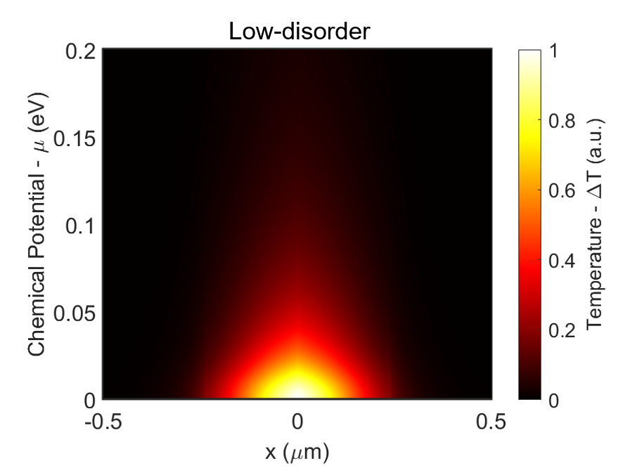
The normalized profiles of the high-disorder (meV) and the low-disorder (meV) graphene photodetectors are shown in Fig 6. The maximum is located at the waveguide center, and decays as one approaches the waveguide sides. Therefore, a strong gradient is present across the graphene sheet, resulting in the generation of a PTE voltage according to Eq. (1). It is noted that drops with rising µ, which is expected since the PTE effect is more dominant in the low µ regime, as was explained in section 3. It is observed that the carrier temperature is slightly more concentrated at low chemical potentials for the low-disorder sheet. A similar trend is seen in the Seebeck coefficient () plots shown in Fig 7(b), where is higher for low-disorder sheets at low chemical potentials. The Seebeck coefficient, and hence the thermoelectric performance, is enhanced in low-disorder graphene Zhou et al. 2015.



Photovoltaic graphene photodetectors function based on the flow of photoexcited carriers in graphene, which makes such photodetectors carrier transit-time limited Gao et al. 2018. On the other hand, PTE graphene photodetectors operate based on the generation of a thermoelectric voltage induced by photoexcited hot carriers in graphene. The operation speed of PTE graphene photodetectors is limited by the carrier cooling rate Tielrooij et al. 2015; Gosciniak et al. 2020; Miseikis et al. 2020, where carriers can re-participate in the photodetection process after adequately cooling down. Interestingly, a high mobility graphene sheet is favorable for photovoltaic photodetectors, since a low mobility sheet limits the speed of carrier flow across graphene, while a low mobility sheet is preferable for PTE graphene photodetectors, as long as the device bandwidth is the only concern. On the other hand, the Seebeck effect, and consequently the thermoelectric performance is degraded at higher disorder Zhou et al. 2015, resulting in a responsivity-bandwidth trade-off for graphene-on-SiO2 PTE detectors that is dictated by the disorder strength.
5.2 Photoresponsivity and Noise Performance
The voltage responsivity () and the current responsivity () of the photodetector are shown in Fig 8. The enhanced thermoelectric performance of low-disorder graphene augments the detector’s photoresponse. The voltage responsivity exceeds 350 V/W and 650 V/W for meV and meV, respectively. It is observed that the responsivity strongly depends on the chemical potential, which is related to the dependence of and on µ. The device performance is optimal when eV, where the Seebeck coefficient and the carrier cooling rate are both high. Consequently, chemical potential tuning is required to acquire the optimum responsivity. The chemical potential of graphene on a substrate can be tuned by thermal annealing Song et al. 2012; Gannett et al. 2011; Romero et al. 2008. The current responsivity is as high as 1.4 A/W (1.1 A/W external) for meV, and 0.7 A/W (0.6 A/W external) for meV.


The highest demonstrated responsivity of a waveguide-integrated graphene-based photodetector is 0.67 A/W at 0.5 V bias, for a m long device Ma et al. 2020. Using high-mobility graphene (meV), the herein proposed device can deliver that responsivity (1.1 A/W external) for a smaller footprint (3.5µm), and is the most compact graphene-based waveguide photodetector reported up-to-date. Moreover, this device operates at the zero-bias condition, while offering CMOS-compatibility and ultra-high-speed beyond 100 GHz. Theoretical responsivities up to 1000 A/W have been reported in Gosciniak et al. 2020 for a waveguide-integrated graphene photodetector, which may be overestimated considering the highest responsivity demonstrated so far, namely 0.67 A/W.
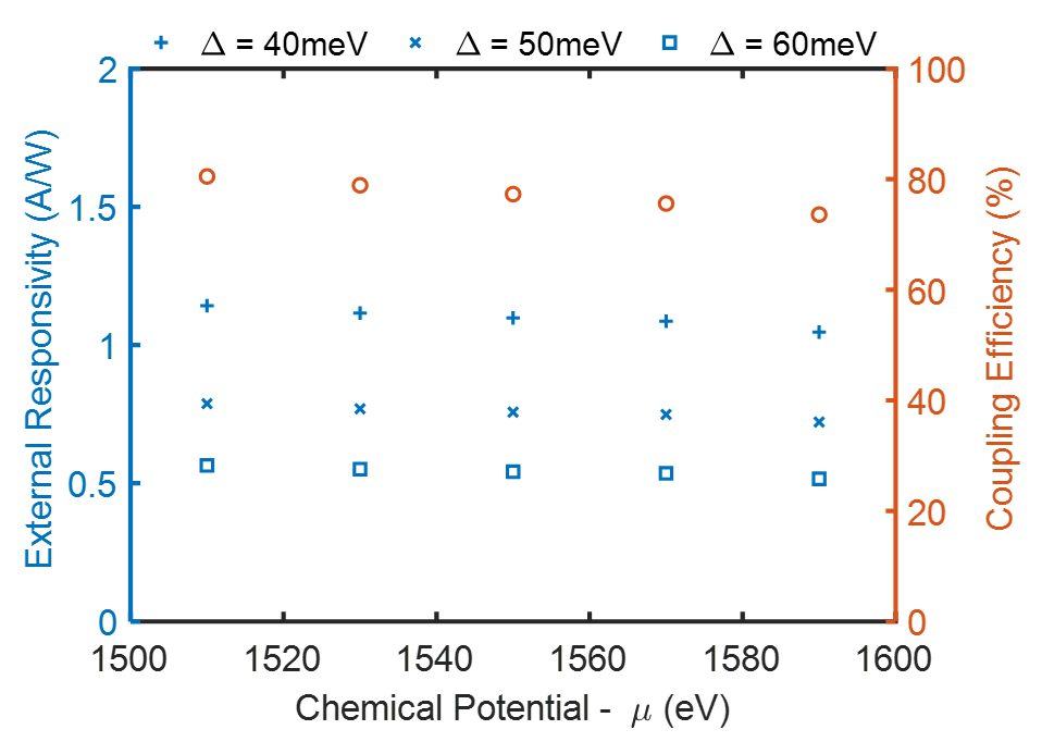
The photodetector exhibits a nearly flat photoresponse across the telecom C-band, as illustrated by the blue markers in Fig 9(a). Here we consider the maximum external responsivity of the photodetectors for comparison, where the external responsivity is defined as the product of the responsivity with the coupling efficiency. It is observed that the responsivity slightly increases at shorter wavelengths following the trend of the coupling efficiency, which is represented by the red markers in Fig 9(a). Certainly, the graphene absorption of the propagating mode increases at longer wavelengths, since the propagating mode becomes more confined in the photodetector waveguide, and the graphene sheet absorbs more of the propagating mode as a result (see supplementary section 3). However, at long wavelengths in this band, the coupling efficiency reduces at a higher rate than the increasing rate of the graphene absorption, which explains the results that we obtain in this study.

Further improvement of the device performance can be achieved by placing graphene on a hexagonal boron nitride (hBN) substrate, or encapsulating graphene between two hBN layers. The Seebeck coefficient of graphene is enhanced by when placed on a hBN substrate Shautsova et al. 2018. This is due to the charge screening role of the hBN spacer layer, which mitigates the influence of the substrate impurities Duan et al. 2016. In addition, the carrier cooling dynamics in graphene-hBN Van der Waals (vdW) heterostructures is dominated by hot carrier coupling to hyperbolic phonon polaritons, not disorder-assisted scattering Tielrooij et al. 2018; Principi et al. 2017; Huang et al. 2020. Experimentally, graphene-on-hBN demonstrated faster cooling dynamics than graphene-on-SiO2 Tielrooij et al. 2018; Golla et al. 2017. Therefore, the cooling pathway introduced by hyperbolic phonon polaritons is more efficient than disorder-assisted scattering, which opens up the possibility for faster optoelectronic devices that are based on graphene-hBN vdW heterostructures.
A transimpedance amplifier is an electronic circuit that converts an input electric current into voltage, and is typically employed in receiver circuits to convert the photodetector current into a voltage reading Abu-Taha and Yazgi 2016. The proposed device can be operated without a transimpedance amplifier Akinwande et al. 2019, since a photovoltage is already generated across the graphene sheet, and can be collected through the two TiN films as was shown in Fig. 8. Moreover, this device does not consume energy, has a zero dark current, zero flicker () noise, and zero shot noise, because of its zero-bias operation Tielrooij et al. 2018; Yurgens 2020; Perepelitsa 2006; Gray et al. 2001; Bahreyni 2009; Miseikis et al. 2020. Therefore, its noise equivalent power (NEP) is determined by the Johnson-Nyquist (thermal) noise:
| (23) |
Where is the variance of the thermal noise voltage per 1 Hz of bandwidth. The NEP is defined as the input signal power that results in an SNR ratio of 1 in a 1 Hz output bandwidth. A low NEP value corresponds to a lower noise floor and a more sensitive detector Mackowiak et al.; Leclercq 2007. Therefore, a low NEP value is an attractive feature for photodetector devices. Fig 9(b) shows the NEP as a function of µ, for meV, meV, and meV. It is noted that the NEP for the low-disorder photodetectors is initially low at low chemical potentials. That is attributed to the remarkably high and small of the low-disorder graphene photodetector in that regime. Nevertheless, the NEP becomes comparatively lower for the high-disorder graphene photodetector at high chemical potentials, where the voltage responsivity of the low-disorder graphene photodetector is relatively low. The voltage responsivity of the the high-disorder graphene photodetector becomes slightly higher than that of the low-disorder graphene photodetector at large µ values, as was illustrated in Fig 8. The resistance of low-disorder graphene is lower than that of high-disorder graphene at all chemical potentials, as was shown in Fig 5; this is supposed to give a lower NEP for the low-disorder graphene at large µ values, but the graphene sheet resistance term () is under the square root in Eq. 23, making the term more effective in determining the NEP.
Considering that the photodetectors are operating in the optimal chemical potential range, µeV, the corresponding NEP values are nearly NEPpW/ for both photodetectors, where we deliberately exclude the NEP values at , in addition to NEP values in its very close proximity, since the chemical potential cannot be exactly zero, as was explained in section 4. These NEP values are an order of magnitude lower than the reported values for other plasmonically-enhanced graphene photodetectors Guo et al. 2020; Muench et al. 2019. Therefore, the zero-bias operation of the proposed photodetector eliminates flicker noise, shot noise and dark current, and as a result, the NEP is minimal. However, in an actual measurement setup, noise from the photodetector makes up a fraction of the total noise, where contributions by other components in the system may be dominant, e.g. amplifier noise Ma et al. 2019, and taking that into account may invalidate the previous comparison. Nonetheless, the intrinsic NEP introduced by this photodetector is ultra-low (<).
5.3 Conclusion
To sum up, a waveguide-integrated graphene photodetector based on the plasmon-induced photothermoelectric effect is proposed. The on-chip photodetector relies on the plasmonic response of titanium nitride (TiN), which is a CMOS-compatible metal nitride that exhibits plasmonic properties similar to gold. Simulations were carried out to optimize the device geometry, and hot carrier transport theory was applied to study the device performance. We conclude that higher device speeds are possible with high-disorder graphene, while a superior thermoelectric performance is achievable using low-disorder graphene. The effect of a varying chemical potential was studied, and it was found out that the device performance is optimal for µeV, because the carrier cooling rate and the Seebeck coefficient are both high in this range. Finally, the device responsivity was calculated, where it was found out that low-disorder graphene is more responsive than the high-disorder graphene, with a responsivity as high as 1.4 A/W (1.1 A/W external) for the low-disorder graphene (meV), and 0.7 A/W (0.6 A/W external) for the high-disorder graphene (meV) photodetectors, at an ultra-compact length of 3.5 µm. This device has the most compact footprint reported for a waveguide-integrated graphene-based photodetector. Moreover, it exhibits a nearly flat photoresponse across the telecom C-band. In addition, the photodetector has an ultra-low intrinsic NEP (<) at the optimal chemical potential range, because of its bias-free operation, which also means that it consumes zero energy. We draw out these conclusions after performing our study on plasmonically-enhanced photothermoelectric graphene photodetectors in a waveguide-integrated configuration. Further advances in graphene deposition methods and quality control of samples will be key in realizing graphene-based optoelectronics as a mainstream industrial technology.
Suppementary Material
See Supplement 1 for supporting content.
References
- Sousa and Achard (2016) Sousa, I. D.; Achard, L.-M. The future of packaging with silicon photonics. 2016.
- Chen et al. (2018) Chen, X.; Milosevic, M. M.; Stanković, S.; Reynolds, S.; Bucio, T. D.; Li, K.; Thomson, D. J.; Gardes, F.; Reed, G. T. The Emergence of Silicon Photonics as a Flexible Technology Platform. Proceedings of the IEEE 2018, 106, 2101–2116.
- Zhang et al. (2012) Zhang, J.; Zhang, L.; Xu, W. Surface plasmon polaritons: physics and applications. Journal of Physics D: Applied Physics 2012, 45, 113001.
- Akinwande et al. (2019) Akinwande, D.; Huyghebaert, C.; Wang, C.-H.; Serna, M. I.; Goossens, S.; Li, L.-J.; Wong, H.-S. P.; Koppens, F. H. L. Graphene and two-dimensional materials for silicon technology. Nature 2019, 573, 507–518.
- Salamin et al. (2018) Salamin, Y.; Ma, P.; Baeuerle, B.; Emboras, A.; Fedoryshyn, Y.; Heni, W.; Cheng, B.; Josten, A.; ; Leuthold, J. 100 GHz Plasmonic Photodetector. ACS Photonics 2018, 5, 3291–3297.
- Goykhman et al. (2016) Goykhman, I.; Sassi, U.; Desiatov, B.; Mazurski, N.; Milana, S.; de Fazio, D.; Eiden, A.; Khurgin, J.; Shappir, J.; Levy, U.; ; Ferrari, A. C. On-Chip Integrated, Silicon–Graphene Plasmonic Schottky Photodetector with High Responsivity and Avalanche Photogain. Nano Letters 2016, 16, 3005–3013.
- Sun and Beling (2019) Sun, K.; Beling, A. High-Speed Photodetectors for Microwave Photonics. Applied Sciences 2019, 9, 623.
- Koester et al. (2006) Koester, S. J.; Member, S.; IEEE,; Schaub, J. D.; Member,; IEEE,; Dehlinger, G.; Chu, J. O. Germanium-on-SOI Infrared Detectors for Integrated Photonic Applications. IEEE Journal of Selected Topics in Quantum Electronics 2006, 12, 1489 – 1502.
- Klamkin et al. (2018) Klamkin, J.; Zhao, H.; Song, B.; Liu, Y.; Isaac, B.; Pinna, S.; Sang, F.; Coldren, L. Indium Phosphide Photonic Integrated Circuits: Technology and Applications. 2018 IEEE BiCMOS and Compound Semiconductor Integrated Circuits and Technology Symposium (BCICTS). 2018; pp 8–13.
- Jung et al. (2016) Jung, Y.; Shim, J.; Kwon, K.; You, J.-B.; Choi, K.; Yu, K. Hybrid integration of III-V semiconductor lasers on silicon waveguides using optofluidic microbubble manipulation. Scientific Reports 2016, 6.
- Xia et al. (2009) Xia, F.; Mueller, T.; ming Lin, Y.; Valdes-Garcia, A.; Avouris, P. Ultrafast graphene photodetector. Nature Nanotechnology 2009, 4, 839–843.
- Koppens et al. (2014) Koppens, F. H. L.; Mueller, T.; Avouris, P.; Ferrari, A. C.; Vitiello, M. S.; Polini, M. Photodetectors based on graphene, other two-dimensional materials and hybrid systems. Nature Nanotechnology 2014, 9, 780–793.
- Gan et al. (2013) Gan, X.; Shiue, R.-J.; Gao, Y.; Meric, I.; Heinz, T. F.; Shepard, K.; Hone, J.; Assefa, S.; Englund, D. Chip-integrated ultrafast graphene photodetector with high responsivity. Nature photonics 2013, 7, 883–887.
- Wang et al. (2013) Wang, X.; Cheng, Z.; Xu, K.; Tsang, H. K.; Xu, J.-B. High-responsivity graphene/silicon-heterostructure waveguide photodetectors. Nature Photonics 2013, 7, 888–891.
- Xie et al. (2018) Xie, C.; Wang, Y.; Zhang, Z.-X.; Wang, D.; Luo, L.-B. Graphene/semiconductor hybrid heterostructures for optoelectronic device applications. Nano Today 2018, 19, 41–83.
- Di Bartolomeo et al. (2018) Di Bartolomeo, A.; Luongo, G.; Iemmo, L.; Urban, F.; Giubileo, F. Graphene–silicon Schottky diodes for photodetection. IEEE Transactions on Nanotechnology 2018, 17, 1133–1137.
- Youngblood et al. (2014) Youngblood, N.; Anugrah, Y.; Ma, R.; Koester, S. J.; Li, M. Multifunctional graphene optical modulator and photodetector integrated on silicon waveguides. Nano letters 2014, 14, 2741–2746.
- Wang et al. (2015) Wang, J.; Cheng, Z.; Chen, Z.; Xu, J.-B.; Tsang, H. K.; Shu, C. Graphene photodetector integrated on silicon nitride waveguide. Journal of Applied Physics 2015, 117, 144504.
- Ma et al. (2019) Ma, P.; Salamin, Y.; Baeuerle, B.; Josten, A.; Heni, W.; Emboras, A.; Leuthold, J. Plasmonically Enhanced Graphene Photodetector Featuring 100 Gbit/s Data Reception, High Responsivity, and Compact Size. ACS Photonics 2019, 6, 154–161.
- Guo et al. (2020) Guo, J.; Li, J.; Liu, C.; Yin, Y.; Wang, W.; Ni, Z.; Fu, Z.; Yu, H.; Xu, Y.; Shi, Y.; Ma, Y.; Gao, S.; Tong, L.; Dai, D. High-performance silicon-graphene hybrid plasmonic waveguide photodetectors beyond 1.55 µm. Light: Science & Applications 2020, 9.
- Muench et al. (2019) Muench, J. E. et al. Waveguide-Integrated, Plasmonic Enhanced Graphene Photodetectors. Nano Letters 2019, 19.
- Ding et al. (2019) Ding, Y.; Cheng, Z.; Zhu, X.; Yvind, K.; Dong, J.; Galili, M.; Hu, H.; Mortensen, N. A.; Xiao, S.; Oxenløwe, L. K. Ultra-compact integrated graphene plasmonic photodetector with bandwidth above 110 GHz. Nanophotonics 2019, 9.
- Lefebvre et al. (2016) Lefebvre, A.; Costantini, D.; Doyen, I.; Lévesque, Q.; Lorent, E.; Jacolin, D.; Greffet, J.-J.; Boutami, S.; ; Benisty, H. CMOS compatible metal-insulator-metal plasmonic perfect absorbers. Optical Materials Express 2016, 6, 2389–2396.
- Catellani and Calzolari (2017) Catellani, A.; Calzolari, A. Plasmonic properties of refractory titanium nitride. Physical Review B 2017, 95.
- TiN (1996) Oyama, S., Ed. The Chemistry of Transition Metal Carbides and Nitrides; Blackie Academic & Professional, 1996.
- Patsalas et al. (2015) Patsalas, P.; Kalfagiannis, N.; Kassavetis, S. Optical Properties and Plasmonic Performance of Titanium Nitride. Materials 2015, 8.
- Gosciniak et al. (2019) Gosciniak, J.; Atar, F. B.; Corbett, B.; Rasras, M. Plasmonic Schottky photodetector with metal stripe embedded into semiconductor and with a CMOS-compatible titanium nitride. Scientific Reports 2019, 9.
- Briggs et al. (2016) Briggs, J. A.; Naik, G. V.; Petach, T. A.; Baum, B. K.; Goldhaber-Gordon, D.; Dionne, J. A. Fully CMOS-compatible titanium nitride nanoantennas. Applied Physics Letters 2016, 108.
- Peters et al. (2010) Peters, E. C.; Lee, E. J. H.; Burghard, M.; ; Kern, K. Gate dependent photocurrents at a graphene p-n junction. Applied Physics Letters 2010, 97, 193102.
- Rao et al. (2011) Rao, G.; Freitag, M.; Chiu, H.-Y.; Sundaram, R. S.; ; Avouris, P. Raman and Photocurrent Imaging of Electrical Stress-Induced p–n Junctions in Graphene. Nano Letters 2011, 5, 5848–5854.
- Mueller et al. (2009) Mueller, T.; Xia, F.; Freitag, M.; Tsang, J.; Avouris, P. Role of contacts in graphene transistors: A scanning photocurrent study. Physical Review B 2009, 79, 245430.
- Jago et al. (2019) Jago, R.; Malic, E.; Wendler, F. Microscopic origin of the bolometric effect in graphene. Physical Review B 2019, 99, 035419.
- Wang et al. (2016) Wang, Y.; Yin, W.; Han, Q.; Yang, X.; Ye, H.; Lv, Q.; ; Yin, D. Bolometric effect in a waveguide-integrated graphene photodetector. Chinese Physics B 2016, 25.
- Vora et al. (2012) Vora, H.; Kumaravadivel, P.; Nielsen, B.; Du, X. Bolometric response in graphene based superconducting tunnel junctions. Applied Physics Letters 2012, 100, 153507.
- Cai et al. (2014) Cai, X.; Sushkov, A. B.; Suess, R. J.; Jadidi, M. M.; Jenkins, G. S.; Nyakiti, L. O.; Myers-Ward, R. L.; Li, S.; Yan, J.; Gaskill, D. K.; Murphy, T. E.; Drew, H. D.; Fuhrer, M. S. Photodetectors based on graphene, other two-dimensional materials and hybrid systems. Nature Nanotechnology 2014, 9, 780–793.
- Basko (2011) Basko, D. A Photothermoelectric Effect in Graphene. Science 2011, 334, 610–611.
- Xu et al. (2009) Xu, X.; Gabor, N. M.; Alden, J. S.; van der Zande, A. M.; ; McEuen, P. L. Photo-Thermoelectric Effect at a Graphene Interface Junction. Nano Letters 2009, 10, 562–566.
- Freitag et al. (2012) Freitag, M.; Low, T.; Xia, F.; Avouris, P. Photoconductivity of biased graphene. Nature Photonics 2012, 7, 53–59.
- Song et al. (2011) Song, J. C. W.; Rudner, M. S.; Marcus, C. M.; Levitov, L. S. Hot Carrier Transport and Photocurrent Response in Graphene. Nano Letters 2011, 11, 4688–4692.
- Chen et al. (2019) Chen, Y.; Li, Y.; Zhao, Y.; Zhou, H.; Zhu, H. Highly efficient hot electron harvesting from graphene before electron-hole thermalization. Science Advances 2019, 5.
- Song et al. (2012) Song, J. C. W.; Reizer, M. Y.; Levitov, L. S. Disorder-Assisted Electron-Phonon Scattering and Cooling Pathways in Graphene. Physical Review Letters 2012, 109, 106602.
- Ma et al. (2014) Ma, Q.; Gabor, N. M.; Anderse, T. I.; Nair, N. L.; Watanabe, K.; Taniguchi, T.; Jarillo-Herrero, P. Competing Channels for Hot-Electron Cooling in Graphene. Physical Review Letters 2014, 112, 247401.
- Chen et al. (2008) Chen, J.-H.; Jang, C.; Adam, S.; Fuhrer, M. S.; Williams, E. D.; Ishigami, M. Charged-impurity scattering in graphene. Nature Physics 2008, 4, 377–381.
- Shautsova et al. (2018) Shautsova, V.; Sidiropoulos, T.; Xiao, X.; Güsken, N. A.; Black, N. C. G.; Gilbertson, A. M.; Giannini, V.; Maier, S. A.; Cohen, L. F.; Oulton, R. F. Plasmon induced thermoelectric effect in graphene. Nature Communications 2018, 9.
- gra (2018) Liu, J.-M., Lin, I.-T., Eds. Graphene Photonics; Cambridge University Press, 2018.
- Pierret (1996) Pierret, R. Semiconductor device fundamentals. 1996.
- Mönch (2017) Mönch, W. In Springer Handbook of Electronic and Photonic Materials; Kasap, S., Capper, P., Eds.; Springer International Publishing: Cham, 2017; pp 1–1.
- Yu et al. (2009) Yu, Y.-J.; Zhao, Y.; Ryu, S.; Brus, L. E.; Kim, K. S.; Kim, P. Tuning the Graphene Work Function by Electric Field Effect. Nano Letters 2009, 9, 3430–3434.
- Naghdi et al. (2019) Naghdi, S.; Sanchez-Arriaga, G.; Rhee, K. Y. Tuning the work function of graphene toward application as anode and cathode. Journal of Alloys and Compounds 2019, 805, 1117 – 1134.
- Lima et al. (2012) Lima, L.; Diniz, J.; Doi, I.; Godoy Fo, J. Titanium nitride as electrode for MOS technology and Schottky diode: Alternative extraction method of titanium nitride work function. Microelectronic Engineering 2012, 92, 86 – 90, 27th Annual Advanced Metallization Conference 2010.
- Fillot et al. (2005) Fillot, F.; Morel, T.; Minoret, S.; Matko, I.; Maîtrejean, S.; Guillaumot, B.; Chenevier, B.; Billon, T. Investigations of titanium nitride as metal gate material, elaborated by metal organic atomic layer deposition using TDMAT and NH3. Microelectronic Engineering 2005, 82, 248 – 253, Proceedings of the ninth european workshop on materials for advanced metallization 2005.
- Pierret (1996) Pierret, R. Semiconductor Device Fundamentals; Addison-Wesley, 1996.
- Shiue et al. (2015) Shiue, R.-J.; Gao, Y.; Wang, Y.; Peng, C.; Robertson, A. D.; Efetov, D. K.; Assefa, S.; Koppens, F. H. L.; Hone, J.; Englund, D. High-Responsivity Graphene–Boron Nitride Photodetector and Autocorrelator in a Silicon Photonic Integrated Circuit. Nano Letters 2015, 15, 7288–7293.
- Lin et al. (2019) Lin, Y. et al. Asymmetric hot-carrier thermalization and broadband photoresponse in graphene-2D semiconductor lateral heterojunctions. Science Advances 2019, 5.
- Shiue et al. (2015) Shiue, R.-J.; Gao, Y.; Wang, Y.; Peng, C.; Robertson, A. D.; Efetov, D. K.; Assefa, S.; Koppens, F. H. L.; Hone, J.; ; Englund, D. High-Responsivity Graphene–Boron Nitride Photodetector and Autocorrelator in a Silicon Photonic Integrated Circuit. Nano Letters 2015, 15, 7288–7293.
- Dorgan et al. (2010) Dorgan, V. E.; Bae, M.-H.; Pop, E. Mobility and saturation velocity in graphene on SiO2. Applied Physics Letters 2010, 97, 082112.
- Phillips and Fisher (2005) Phillips, N.; Fisher, R. Specific Heat. Encyclopedia of Condensed Matter Physics. 2005; pp 8–19.
- Gosciniak et al. (2020) Gosciniak, J.; Rasras, M.; Khurgin, J. B. Ultrafast Plasmonic Graphene Photodetector Based on the Channel Photothermoelectric Effect. ACS Photonics 2020, 7, 488–498.
- Gosciniak et al. (2016) Gosciniak, J.; Justice, J.; Khan, U.; Corbett, B. Study of TiN nanodisks with regard to application for Heat-Assisted Magnetic Recording. MRS Advances 2016, 1, 317–326.
- (60) Lumerical, Graphene surface conductivity material model. https://support.lumerical.com/hc/en-us/articles/360042244874-Graphene-surface-conductivity-material-model.
- Falkovsky (2008) Falkovsky, L. A. Optical properties of graphene. Journal of Physics: Conference Series 2008, 129, 012004.
- Ooi et al. (2017) Ooi, K. J. A.; Leong, P. C.; Ang, L. K.; Tan, D. T. H. All-optical control on a graphene-on-silicon waveguide modulator. Scientific Reports 2017, 7.
- Romero et al. (2008) Romero, H. E.; Shen, N.; Joshi, P.; Gutierrez, H. R.; Tadigadapa, S. A.; Sofo, J. O.; Eklund, P. C. n-Type Behavior of Graphene Supported on Si/SiO2 Substrates. ACS Nano 2008, 2, 2037–2044, PMID: 19206449.
- (64) Lumerical, Working with lossy modes and dB/m to k conversion. https://support.lumerical.com/hc/en-us/articles/360034917493-Working-with-lossy-modes-and-dB-m-to-k-conversion.
- Miseikis et al. (2020) Miseikis, V.; Marconi, S.; Giambra, M. A.; Montanaro, A.; Martini, L.; Fabbri, F.; Pezzini, S.; Piccinini, G.; Forti, S.; Terres, B., et al. Ultrafast, Zero-Bias, Graphene Photodetectors with Polymeric Gate Dielectric on Passive Photonic Waveguides. ACS nano 2020, 14, 11190–11204.
- Bao et al. (2009) Bao, Q.; Zhang, H.; Wang, Y.; Ni, Z.; Yan, Y.; Shen, Z. X.; Loh, K. P.; Tang, D. Y. Atomic-layer graphene as a saturable absorber for ultrafast pulsed lasers. Advanced Functional Materials 2009, 19, 3077–3083.
- Tielrooij et al. (2015) Tielrooij, K. J.; Piatkowski, L.; Massicotte, M.; Woessner, A.; Ma, Q.; Lee, Y.; Myhro, K. S.; Lau, C. N.; Jarillo-Herrero, P.; van Hulst, N. F.; Koppens, F. H. L. Generation of photovoltage in graphene on a femtosecond timescale through efficient carrier heating. Nature Nanotechnology 2015, 10, 437–443.
- Dawlaty et al. (2008) Dawlaty, J. M.; Shivaraman, S.; Chandrashekhar, M.; Rana, F.; Spencer, M. G. Measurement of ultrafast carrier dynamics in epitaxial graphene. Applied Physics Letters 2008, 92, 042116.
- Wang et al. (2020) Wang, L.; Makk, P.; Zihlmann, S.; Baumgartner, A.; Indolese, D. I.; Watanabe, K.; Taniguchi, T.; Schönenberger, C. Mobility Enhancement in Graphene by in situ Reduction of Random Strain Fluctuations. Phys. Rev. Lett. 2020, 124, 157701.
- Yan and Fuhrer (2011) Yan, J.; Fuhrer, M. S. Correlated Charged Impurity Scattering in Graphene. Phys. Rev. Lett. 2011, 107, 206601.
- Zhou et al. (2015) Zhou, B.; Zhou, B.; Zeng, Y.; Zhou, G.; Ouyang, T. Spin-dependent Seebeck effects in a graphene nanoribbon coupled to two square lattice ferromagnetic leads. Journal of Applied Physics 2015, 117, 104305.
- Gao et al. (2018) Gao, Y.; Tao, L.; Tsang, H. K.; Shu, C. Graphene-on-silicon nitride waveguide photodetector with interdigital contacts. Applied Physics Letters 2018, 112, 211107.
- Gannett et al. (2011) Gannett, W.; Regan, W.; Watanabe, K.; Taniguchi, T.; Crommie, M. F.; Zettl, A. Boron nitride substrates for high mobility chemical vapor deposited graphene. Applied Physics Letters 2011, 98, 242105.
- Ma et al. (2020) Ma, Z.; Kikunaga, K.; Wang, H.; Sun, S.; Amin, R.; Maiti, R.; Tahersima, M. H.; Dalir, H.; Miscuglio, M.; Sorger, V. J. Compact graphene plasmonic slot photodetector on silicon-on-insulator with high responsivity. ACS Photonics 2020, 7, 932–940.
- Duan et al. (2016) Duan, J.; Wang, X.; Lai, X.; Li, G.; Watanabe, K.; Taniguchi, T.; Zebarjadi, M.; Andrei, E. Y. High thermoelectricpower factor in graphene/hBN devices. Proceedings of the National Academy of Sciences 2016, 113, 14272–14276.
- Tielrooij et al. (2018) Tielrooij, K.-J.; Hesp, N. C.; Principi, A.; Lundeberg, M. B.; Pogna, E. A.; Banszerus, L.; Mics, Z.; Massicotte, M.; Schmidt, P.; Davydovskaya, D., et al. Out-of-plane heat transfer in van der Waals stacks through electron–hyperbolic phonon coupling. Nature nanotechnology 2018, 13, 41–46.
- Principi et al. (2017) Principi, A.; Lundeberg, M. B.; Hesp, N. C.; Tielrooij, K.-J.; Koppens, F. H.; Polini, M. Super-Planckian electron cooling in a van der Waals stack. Physical review letters 2017, 118, 126804.
- Huang et al. (2020) Huang, P.; Riccardi, E.; Messelot, S.; Graef, H.; Valmorra, F.; Tignon, J.; Taniguchi, T.; Watanabe, K.; Dhillon, S.; Placais, B., et al. Ultra-long carrier lifetime in neutral graphene-hBN van der Waals heterostructures under mid-infrared illumination. Nature communications 2020, 11, 1–9.
- Golla et al. (2017) Golla, D.; Brasington, A.; LeRoy, B. J.; Sandhu, A. Ultrafast relaxation of hot phonons in graphene-hBN heterostructures. APL Materials 2017, 5, 056101.
- Abu-Taha and Yazgi (2016) Abu-Taha, J.; Yazgi, M. A 7 GHz compact transimpedance amplifier TIA in CMOS 0.18 µm technology. Analog Integrated Circuits and Signal Processing 2016, 86, 429–438.
- Tielrooij et al. (2018) Tielrooij, K.; Castilla, S.; Terres, B.; Autore, M.; Viti, L.; Li, J.; Nikitin, A.; Vitiello, M. S.; Hillenbrand, R.; Koppens, F. H. L. Highly sensitive, ultrafast photo-thermoelectric graphene THz detector. 2018 43rd International Conference on Infrared, Millimeter, and Terahertz Waves (IRMMW-THz). 2018; pp 1–3.
- Yurgens (2020) Yurgens, A. Large Responsivity of Graphene Radiation Detectors with Thermoelectric Readout: Results of Simulations. Sensors 2020, 20.
- Perepelitsa (2006) Perepelitsa, D. V. Johnson noise and shot noise. Dept. of Physics, MIT 2006,
- Gray et al. (2001) Gray, P. R.; Hurst, P.; Meyer, R. G.; Lewis, S. Analysis and design of analog integrated circuits; Wiley, 2001.
- Bahreyni (2009) Bahreyni, B. In Fabrication and Design of Resonant Microdevices; Bahreyni, B., Ed.; Micro and Nano Technologies; William Andrew Publishing: Norwich, NY, 2009; pp 129 – 141.
- (86) Mackowiak, V.; Peupelmann, J.; Ma, Y.; Gorges, A. NEP – Noise Equivalent Power. THORLABS.
- Leclercq (2007) Leclercq, S. Discussion about Noise Equivalent Power and its use for photon noise calculation. 2007.