Trigonal Warping, Satellite Dirac Points and Multiple Field Tuned Topological Transitions in Twisted Double Bilayer Graphene
Abstract
We show that the valley Chern number of the low energy band in twisted double bilayer graphene can be tuned through two successive topological transitions, where the direct band gap closes, by changing the electric field perpendicular to the plane of the graphene layers. The two transitions with Chern number changes of and can be explained by the formation of three satellite Dirac points around the central Dirac cone in the moirBrillouin zone due to the presence of trigonal warping. The satellite cones have opposite chirality to the central Dirac cone. Considering the overlap of the bands in energy, which lead to metallic states, we construct the experimentally observable phase diagram of the system in terms of the indirect band gap and the anomalous valley Hall conductivity. We show that while most of the intermediate phase becomes metallic, there is a narrow parameter regime where the transition through three insulating phases with different quantized valley Hall conductivity can be seen. We systematically study the effects of variations in the model parameters on the phase diagram of the system to reveal the importance of particle-hole asymmetry and trigonal warping in constructing the phase diagram. We also study the effect of changes in interlayer tunneling on this phase diagram.
I Introduction
The ability to experimentally control the angle of twist between layers of two-dimensional materials placed on top of each other has led to the field of twistronics: the manipulation of electronic properties of materials by controlling the twist angle Cao et al. 2018a; Carr et al. 2017. The materials can range from graphene Bistritzer and MacDonald 2011 or few layers of graphene Shen et al. 2020; Suárez Morell et al. 2013, to graphene-boron nitride heterostructures Spanton et al. 2018 to transition metal dichalcogenides Zhang et al. 2020, expanding the class of Van der Waals bonded two-dimensional materials Novoselov et al. 2016 with interesting and tunable electronic properties. The most celebrated member of this family is the twisted bilayer graphene, where the system shows an almost flat band around particular twist angles called magic angles Bistritzer and MacDonald 2011; Cao et al. 2018a; Cao et al. 2018b. The presence of strongly correlated phases like superconductivity Cao et al. 2018a; Yankowitz et al. 2019, correlated insulator Cao et al. 2018b, magnetism Sharpe et al. 2019; Po et al. 2018 etc. in these materials around the magic angle has led to a surge in both theoretical and experimental activity in this field.
Twisted double bilayer graphene (TDBLG) Koshino 2019; Chebrolu et al. 2019; Haddadi et al. 2020 consists of two layers of bilayer graphene (which are themselves stacks of two layers of graphene) placed on top of each other and rotated with respect to each other. In these systems, the twist angle where flat bands are formed can be tuned relatively easily by application of pressure Lin et al. 2020. Correlated insulating states Liu et al. 2020; Burg et al. 2019; Adak et al. 2020 with possible magnetic order have been seen in these systems near magic angle. On doping, the system has also shown superconductor-like phasesLiu et al. 2020.
Electric field applied perpendicular to the plane of the material is widely used in simple bilayer graphene to modify its electronic properties, from tunable band gaps Zhang et al. 2009; Castro et al. 2010 to occurrence of Lifshitz transitions Varlet et al. 2015; Varlet et al. 2014 in the Fermi surface of the system. The electronic properties of TDBLG in the presence of electric field have been studied previously both theoretically Chebrolu et al. 2019; Lee et al. 2019 and experimentally Liu et al. 2020; Burg et al. 2019; Adak et al. 2020. While a simple minimal model having particle hole symmetry has been proposed to describe this system Koshino 2019; Chebrolu et al. 2019; Burg et al. 2019, it has been experimentally shown that the metallic and insulating behaviour of the system is actually consistent with a more detailed model which does not have particle-hole symmetry Adak et al. 2020.
In this paper, we study the electronic properties of the TDBLG as a function of the twist angle and the applied electric field (or equivalently the potential difference between the layers) and present a topological phase diagram of the system. We show that as a function of electric field, the system undergoes two topological transitions, where the direct band gap between the conduction and the valence band of the system vanishes. The valley Chern number of the low energy valence band changes by and at these two transitions respectively. There are two ways to stack layers of AB bilayer graphene and twist them: the AB-AB stacking and the AB-BA stacking. We find that the Chern numbers for the AB-AB stacking and the AB-BA stacking are different; however, the changes in the Chern numbers across the transition are same for both stacking.
While the Chern numbers for TDBLG have been predicted before Chebrolu et al. 2019, in this paper, we provide an explanation for the transitions using the splitting of the single Dirac point into four different Dirac points. Of these, the central one at has opposite chirality to the three satellite Dirac points. This is similar to the Lifshitz transition in a BLG in perpendicular electric field. However, unlike BLG, in presence of tunneling between the twisted layers, the location of these Dirac points can be moved up or down in energy by tuning the electric field, resulting in non-trivial topological transitions. At low and intermediate twist angles , these points are separated in energy. As a function of increasing electric field, the gap first closes at the satellite Dirac points, leading to a Chern number change of , while the gap closing at higher electric field occurs at the central Dirac point, leading to a Chern number change of . These two transitions come closer and almost merge at large twist angles. The formation of the satellite Dirac points and the separation of the two transitions in the system are driven by the presence of trigonal warping, which is known to create satellite Dirac points in simple bilayer graphene as well Rozhkov et al. 2016.
While the direct band gap and the Chern number are well defined theoretical quantities for TDBLG, the overlap of the bands in energy space implies that they are not directly related to observable quantities. Focusing on the undoped system, we study the indirect band gap, which can be directly linked to transport properties, and the anomalous valley Hall conductivity which can be measured in non-local transport measurements. The overlapping bands lead to Fermi surface and metallic behaviour with non-quantized values of the anomalous valley Hall conductivity in two regimes: (a) low twist angles and low electric fields and (b) high twist angles and high electric fields. However, the system remains insulating at high twist angle and low electric field as well as at low twist angle and high electric fields, with associated quantized valley Hall conductivity. In between, there is a regime of intermediate twist angles where the system passes between three gapped states through two gap closing transitions, revealing the intermediate phase with non-trivial quantized valley Hall conductivity.
The hopping parameters in a TDBLG are amenable to change under pressure, which is one of the reasons it is easier to tune this system’s electronic properties. Keeping this in mind, we also do an extensive survey of how the phase diagram changes as various hopping parameters in the model are varied. We find that the particle-hole symmetric minimal model completely misses the phenomenology of gap closing at finite electric fields. We show that while breaking the particle hole symmetry results in a single transition, the presence of the trigonal warping term is crucial to obtain the phenomenology of multiple transitions with the pattern of Chern number changes seen in this system. We also study how the phase diagram changes with the ratio of inter-plane hoppings between twisted layers and find that decreasing the ratio makes the intermediate gapped phase more (less) visible in AB-AB (AB-BA) stacked TDBLG.
We now provide a brief road map of the paper. In section II, we describe the model for the band structure of TDBLG in detail, introducing all the relevant parameters in the process. In section III, we present the band structure and the direct bandgap of the system as a function of the twist angle and the electric field and find multiple gap-closing transitions. In section IV, we discuss the Chern numbers of the low lying bands in the system. In section V, we focus on the indirect band gap and the valley Hall conductivity and present the phase diagram in terms of these observable quantities. In section VI, we discuss the variation of the phase diagram with the model parameters before concluding with a summary of our key results.
II Models of TDBLG
Twisted double bilayer graphene is formed by stacking two layers of bilayer graphene (BLG) on top of each other, and rotating the layers with respect to each other. Before we start describing model Hamiltonians for twisted systems, let us review the Hamiltonian for a single Bernal (AB) stacked bilayer graphene.
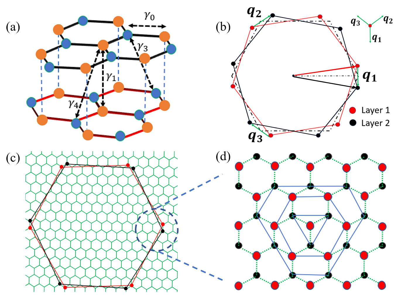
The AB stacked bilayer graphene consists of honeycomb lattices of graphene layers, where the sublattice of the top layer lies directly above the sublattice of the bottom layer and the sublattice of the top layer lies at the center of the bottom layer hexagon, as shown in Fig 1(a). One of the main parameters of the tight-binding Hamiltonian for the bilayer graphene is the in-plane nearest neighbour hopping along the graphene sheets, , leading to a graphene Fermi velocity of Geim and Novoselov 2007. The inter-layer hopping is dominated by the hopping between the and sublattice sites which lie on top of each other, with a tunneling amplitude, Koshino 2019; Malard et al. 2007; Zhang et al. 2008; Castro Neto et al. 2009. Due to this strong tunnel-coupling, the sites on sublattice in the top layer and sublattice in the bottom layer which are just on top of each other are called dimerized sites, while the sublattice sites in the top layer and sublattice sites in the bottom layer are called non-dimerized sites.
In addition to the main hopping parameters described above, there are three more parameters in the tight binding Hamiltonian of a bilayer graphene. The most important of these is the interlayer hopping between the non-dimerized sites in the top and bottom layer, . This trigonal warping term reduces the symmetry of the low energy band dispersion near the Dirac points from an azimuthal symmetry to a symmetry. We will later see that this plays an important role in determining the topological phases of TDBLG in electric field. The value of ranges between and in the literature Malard et al. 2007; Kuzmenko et al. 2009; Rozhkov et al. 2016. There is also a hopping between the dimerized site in one layer and a non-dimerized site in another layer, , with values ranging between and Kuzmenko et al. 2009; Castro Neto et al. 2009; McCann and Koshino 2013. The final parameter is a potential difference between dimerized and non-dimerized sites, . These hopping parameters are also clearly shown in Fig. 1(a).
Using a four component basis consisting of sublattices , and expanding around the Dirac point in a particular valley (say with valley index ), the AB bilayer graphene Hamiltonian can be written as
| (1) |
where
| (2) |
Here , where the momenta are measured from the Dirac point. , , are related to the hopping amplitudes through , where Koshino 2019 is the graphene lattice constant. We note that both and breaks the particle-hole symmetry of the low energy dispersions in the model, while introduces a trigonal warping to the band structure. The Hamiltonian for the valley can be obtained by putting , while for a stacking, and will exchange their positions and will get conjugated to give .
As mentioned earlier, there are two ways to stack layers of AB bilayer graphene and twist them: the AB-AB stacking and the AB-BA stacking. Here, the ordered list of sublattice indices indicate the dimerized sites in each layer, starting from the top. At zero twist angle, the strongest interlayer tunnelings naturally occur between these sublattices in the respective layers. In both cases, the twist angle between the bilayer graphene sheets lead to a tiling of the original graphene Brillouin zone by smaller moirBrillouin zones(MBZ), as shown in Fig. 1(c).
To understand the structure of the moirBrillouin zone, we consider the Brillouin zones of the top and bottom bilayer graphene, rotated about each other by an angle , as shown by the red and black hexagons in Fig. 1(b). One can also consider a reference Brillouin zone, shown by the dashed hexagon in Fig. 1(b), so that the Brillouin zones of the top and bottom layer are rotated by with respect to this reference. The Dirac points in the two layers are now separated from each other by wave vectors , which are aligned at angles of with respect to each other. The difference in momentum between nearby Dirac points in the two layers sets the scale of the moirBrillouin zone to be where is the graphene Brillouin zone vector and is the twist angle. We will use the standard notation with a subscript to denote the high symmetry points of the moirBrillouin zone, e.g. the moirBrillouin zone center is denoted by .

If we start with electrons in the top BLG with momentum in the moirBrillouin zone, the interlayer hopping between the twisted layers couples this electron to electrons in the lower BLG in the three nearest moirBrillouin zones with momenta , with . This is shown clearly in Fig. 1(b). The wave vectors shown in Fig. 1 are related to each other by the moirreciprocal lattice vectors. Thus the minimum size of the Hamiltonian matrix is ( BLG Hamiltonians with matrix for each). For AB-AB stacking, this can be written as
| (3) |
where is the BLG Hamiltonian written in a co-ordinate system which is rotated by an angle , with , where is the azimuthal angle. Note that we use the symmetric reference frame about which the top and bottom are rotated by . Here
| (4) |
and and are the interlayer hopping between and AB sites respectively. There are a wide range of values used for and in the literature, with some consensus around and Lee et al. 2019; Koshino et al. 2018; Nam and Koshino 2017; Uchida et al. 2014; Moon and Koshino 2013; Chebrolu et al. 2019; Dai et al. 2016; Wijk et al. 2015.
We note that this constitutes the lowest order terms in the Hamiltonian. Each of these three points would be connected by the interlayer tunneling to points at in other moirBrillouin zones, forming a Hamiltonian matrix of ever-increasing size. In general one should carry out the tiling of the full graphene Brillouin zone with the moirBrillouin zones. The momentum points which get connected in this process are shown in Fig. 1(d), where red dots indicate electrons in top BLG while black dots indicate electrons in the bottom BLG. In practice, as shown by Bistritzer et. al Bistritzer and MacDonald 2011, one can truncate this expansion at reasonably low sizes to get accurate description of low energy bands. In our calculations, we work with sized matrices, which correspond to taking seven layers of nearby shells moirBrillouin zones. This ensure low energy dispersion error below .

We note that the Hamiltonian for the AB-BA stacking can be obtained from Eq. 3 by replacing the lower three s by . The addition of a perpendicular electric field is modeled as a uniform potential difference across the layers, with the topmost layer having a potential and the lowermost layer having a potential . In the Hamiltonian, this corresponds to augmenting ( or ) of the top (bottom) BLG layer by a potential term , where
| (5) |
The detailed model which we use can be replaced by a simpler “minimal” model to obtain some of the qualitative properties of TDBLG Koshino 2019; Chebrolu et al. 2019. In our notation, this corresponds to setting , and to zero. The explicit dependence of the Hamiltonian on the twist angle is also neglected in the minimal model; i.e. is set to . We would however like to note that the minimal model imposes additional particle-hole symmetry Song et al. 2019 and gets some of the qualitative features of experiments wrong, as shown in Ref. Adak et al. 2020; Liu et al. 2020. In this paper, we will see that the minimal model fails to capture the full complexity of the topological phase diagram of the system.
III Electronic Structure and Band Gap in TDBLG

We first consider the electronic structure of twisted double bilayer graphene, focusing on the two low energy bands close to zero energy. While we will later look at how the electronic properties change with system parameters, in this section we will use the parameters in Ref. Koshino 2019 to get a picture of the electronic structure in this system; i.e. we will use , , , , for the bilayer graphene parameters and and for the interlayer tunneling parameters of the TDBLG.
III.1 AB-AB stacked TDBLG
Let us first focus our attention on AB-AB stacked TDBLG. While the experimental focus on the twisted systems has been concentrated around , in this paper we will expand our search to explore the system at twist angles from to .
The band dispersions of the system along the high symmetry axes at a low twist angle of (close to magic angle) is shown for increasing electric fields corresponding to potential differences of and in Fig. 2(a) -(d) respectively. The conduction band dispersion and the valence band dispersion are plotted in red and blue colors respectively. At zero external electric field, Fig. 2(a) shows that the bands touch each other at two points between the and points Koshino 2019. To understand the variation of the band structure with electric fields, it is useful to focus on the gap between the conduction and valence band dispersions at the point in the moirBrillouin zone. This is large at . With increasing electric field, the gap decreases at , and is very small at , as seen in Fig. 2(b) and (c) . At larger electric field, the gap increases again, as seen from the dispersion at in Fig. 2(d). Thus, there is at least one gap closing transition at a finite electric field at low twist angles. Note that the gap closes only at the point and not at the point; since the gap vanishes at odd number of points, one can expect a change in the topology of the bands at the gap closing point.
In Fig. 2(e)-(h), we plot the band dispersion of the system at an intermediate twist angle of for increasing and respectively. The key difference from the low twist angle of is that in this case, there are no gap closings at zero electric field, as seen in Fig. 2(e). From Fig. 2(f) and Fig. 2(g), we see that the gap at point continuously decreases at , and closes around . The gap increases at higher electric fields, as seen from the dispersion at in Fig. 2(h). We plot the band dispersion at a relatively higher twist angle of for increasing and in Fig. 2(i)-(l) respectively. The pattern here is very similar to the case of , with the gap closing around , before increasing once again.

The gap closings motivate us to look at the direct band gap between the valence and conduction bands as a function of electrostatic potential difference and twist angle. We define the direct band gap between the bands as
| (6) |
i.e. the minimum of the difference between the dispersions at each point in the first MBZ. In Fig. 3(a), we show a color plot of the direct band gap of the system as a function of and the twist angle . We see two distinct lines of zero direct gap in the plane: one starting at a finite at , increasing to around , before going down at large angles. The second line starts from at , rises sharply and almost merges with the earlier line around . These lines are clearly visible as black contours in the color plot. We note that for angles below , the second line continues on the axis, as the system is gapless in the absence of an electric field. This can also be seen from the line-cuts along the axis shown in Fig. 3(b), where the gap at is at . The twist angles can then be divided into three regimes depending on the behaviour of the gap closing transitions: (i) the low angle regime, from to , where there is no gap at zero electric field. The gap increases with before coming down and closing at the point at a finite electric field. A representative line cut at is shown in Fig. 3(b) with solid black line. In this case the gap closes at . (ii) The intermediate angle range, from to , where the direct band gap is finite at , and then goes through two gap closing transitions. A representative line cut is shown at in 3(b) with a dashed red line. Here the gap closes first at , then rises again before closing at . Beyond this point the gap rises once again, as seen in the figure. (iii) A large angle regime from onwards, where the two transitions have come so close to each other, that for all practical purposes, we will see it as a single transition. This is shown in the dash-dotted blue line in Fig. 3(b), corresponding to a line cut at , where the common gap closing happens around . We note that the gap closing transitions are absent in the particle-hole symmetric minimal model, where the valence and conduction bands remain gapped at all finite electric fields at all angles (Fig. 11(a)).
We have two distinct gap-closing transitions in the plane. While the upper line of transition matches with the gap closing at the point, the lower line requires further investigations to understand its origin. Clearly the gap does not close at one of the high symmetry points, since the band dispersions of Fig. 2 do not hint at a second gap closing transition at finite electric fields. To understand this transition, we note that the Dirac point in a standard bilayer graphene in an electric field splits into a central Dirac cone and three satellite Dirac cones due to the presence of the trigonal warping term Rozhkov et al. 2016 in the dispersion of a single bilayer graphene. The associated Lifshitz transitions and the resultant quantum Hall degeneracy breaking Varlet et al. 2015; Zhang et al. 2009 have been observed experimentally. A similar situation is arising here. At intermediate angles, along the lower dark line in Fig. 3(a), the gap is closing at the three satellite Dirac points around the point. The gap then opens up again and closes at the central Dirac point ( point) at a larger value of , corresponding to the second transition. Since the satellite Dirac points do not lie on the high symmetry axes, this does not show up in Fig. 2.
To see this clearly, in Fig. 4 (a) -(e), we show a dimensional plot of the band dispersion around the point for a system with twist angle for AB-AB stacked TDBLG, where the system has two clear gap-closing transitions at and respectively. In Fig. 4 (a), we show the situation at , before crossing the first transition point. The three satellite Dirac like points in the conduction(valence) band have a lower (higher) dispersion, and consequently a lower momentum dependent direct gap, , than the point. The corresponding color plot of the the momentum dependent gap is shown in Fig. 4 (f), where it is clear that the lowest gap is not at the point. Fig. 4 (b) depicts the situation at at the first transition point. The satellite Dirac points in the conduction and valence bands touch each other driving the direct band gap to zero, as seen in Fig. 4 (g). As is increased to in Fig. 4 (c), the satellite Dirac points in the valence and conduction bands move away from each other, leading to a finite gap in the system (see Fig. 4 (h)). At the same time, the dispersions of the valence and the conduction band at the central Dirac point are moving towards each other in this regime of . In Fig. 4 (d), at , the two bands touch each other through a single Dirac cone at the point, leading to a second gap closing, as shown in Fig. 4(i). The satellite Dirac points are gapped out at this value of . On increasing further to , both the satellite and the central Dirac point becomes gapped, as seen in Fig. 4 (e) and (j).
The clear understanding of the mechanism of multiple transitions is a key new result in this paper. While the satellite Dirac points are also formed in a BLG in perpendicular electric field, they do not drive any transitions in that case, since the bands get further and further away from each other with increasing electric fields. This description of the mechanism of the transitions will also help us understand the topological changes that are occuring at these transitions in the following sections. We note that the trigonal warping plays a key role in forming the four Dirac points resulting in these transitions. This assertion will be strengthened later, when we systematically study the effects of different band parameters on the phase diagram.
III.2 AB-BA stacked TDBLG
We now turn our attention to the electric field dependent band structure of the AB-BA stacked twisted double bilayer graphene. The picture that emerges here is similar to the case of AB-AB stacked materials, with important differences at low twist angles.
The band dispersion of the system at a low twist angle of is plotted in Fig 5(a)-(d) for , , and respectively. The direct bandgap is finite at zero electric field in this case, in contrast to the situation for the AB-AB stacked TDBLG. The band gap at the point gradually goes down with increasing till it closes around . Beyond this, the gap opens up again as seen at in Fig 5 (d). Fig 5 (e) -(h) shows the band structure with increasing for , while Fig 5 (i) -(l) shows this for . The trends are similar with the gap closing around for and around for .
The direct bandgap for the AB-BA stacking is shown as a color plot in the plane in Fig. 3(c). The trends are very similar to that of the AB-AB stacking, with the exception that the band gap is finite at low twist angles in zero electric field. The twist angles can once again be divided into three regions based on the qualitative dependence of the direct band gap with , similar to the case of AB-AB stacking. This is shown in Fig. 3(d) with three representative line-cuts at (solid black line), (red dashed line) and (blue dash-dotted line).
While the general behaviour of the gap in the plane is similar for AB-AB and AB-BA stacking, there is a crucial difference at low twist angles. While the AB-AB stacked TDBLG has zero direct band gap at zero electric field, the AB-BA stacking shows a finite band gap even at zero electric field in this regime.

IV Topological transitions and phase diagram
The closing of band-gaps without any associated change in symmetry of the system in twisted double bilayer graphene points to the possibility that these gap closings are associated with transitions in topological character of the bands. We now focus on the topological phase diagram of the system by studying the Chern numbers of the bands in the plane
In TDBLG, due to the possible band crossings, the total Berry phase has to be constructed by including all bands upto a certain band, with the highest band index being . The matrix-valued Berry connection and the corresponding Berry curvature are given by
| (7) |
where is the Bloch wavefunction of the corresponding band, and , run over band indices upto . The total Chern number of the bands Hatsugai 2005 is then defined by
| (8) |
This is well defined when the next higher band dispersion is at a finite direct gap from the band being considered. Thus, in our phase diagram, this can be uniquely defined for the valence/conduction band at all points other than at the points where the direct gap closes. Note that this is the Chern number for the mini-band around the valley of the original graphene Brillouin zone. One can do a similar construction for the bands around the valley of the graphene Brillouin zone.
IV.1 AB-AB stacked twisted double bilayer graphene

Let us first consider the Chern number of the valence band of an AB-AB stacked TDBLG around the valley of the original graphene Brillouin zone. The topological phase diagram (or the Chern number as a function of and ) is plotted as a color plot in Fig. 6(a). At low twist angle, the band is trivial exactly at . At an infinitesimal , it has a Chern number of . As is increased, the Chern number jumps to as soon as one crosses the gap closing point. This is clearly seen in the line-cut along the axis at a fixed in Fig. 6(b) ( black solid line). At intermediate angles, where the system undergoes two gap closing transitions, the band is trivial as is increased, until one hits the first transition, when the Chern number jumps to , and then it jumps back to , when the second transition point is crossed. This is clearly seen in the line-cut along the axis at a fixed in Fig. 6(b) (red dashed line). Finally, at large twist angle these two transitions are so close that for all practical purposes, the Chern number jumps from to . However, even at an angle of , there are actually two jumps, one from to and the other from to , as seen in the line cut in Fig. 6(b) ( blue dot-dashed line), although the small regime of between the two jumps would make it impossible to see this in experiments. We note that the Chern number for the conduction band is the negative of the Chern number of the valence band for AB-AB stacked TDBLGChebrolu et al. 2019, and hence a similar looking phase diagram can be constructed by considering the Chern number of the conduction band.

The change in the Chern number of the bands can be understood from the picture of Dirac cones ( a central one at point and three satellite cones around it) in TDBLG, which drove the two gap closing transitions in the system. The satellite Dirac cones each carry a chirality index of , while the central Dirac cone carries an opposite chirality index of (for the valence band). As the electric field is increased at intermediate and high twist angles, the first gap closing transition occurs when the bands touch at the satellite Dirac points. The presence of three gap closing points with a chirality index of (i.e. a Berry monopole of strength at the gap closing point) explains the jump in the Chern number by . The second transition, which is mediated by the band touching at the central Dirac cone at point, corresponds to a Berry monopole of , and hence the Chern number jumps by at this transition. At low twist angles, as we have said before, the first transition is shifted to infinitesimally small electric fields, and hence the band has a Chern number of at low electric fields, before hitting the transition mediated by band touching at the central Dirac point, with the Chern number jumping to .
We would like to note that the above Chern numbers are calculated for bands around the valley. Similarly, bands around the valley have Chern numbers, which are negative of the valley Chern numbers. This is shown in Fig. 7(a), where the Chern number is plotted as a function of for . Since these bands are degenerate, there is no net Chern number of the system. However, the system will show anomalous valley Hall effect if the valley degeneracy is broken. Fig. 7(a) also shows that for AB-AB stacked TDBLG, the Chern number of the bands in each valley change sign if the direction of the electric field is reversed.
We thus obtain a complete understanding of the Chern number jumps in the AB-AB stacked TDBLG in terms of the splitting of the bilayer Dirac point into a central Dirac point and satellites due to trigonal warping.
IV.2 AB-BA stacked twisted double bilayer graphene
While the basic picture of gap closing transitions is very similar in AB-AB and AB-BA stacked TDBLG, they differ quite a bit when it comes to the topological phase diagram. For the AB-BA stacking, we once again focus on the Chern number of the valence band around the point in the graphene Brillouin zone, and construct a phase diagram in the plane based on the Chern number of the valence band. In this case, contrary to the AB-AB stacking, the Chern number of the valence and the conduction bands are same Chebrolu et al. 2019, and hence a similar phase diagram would be obtained if the Chern number of the conduction band is studied.
The Chern number of the AB-BA stacked TDBLG is shown in a color plot in the plane in Fig. 6 (c). At intermediate twist angles, the valence band has a Chern number at zero electric field. This is different from the AB-AB stacking, where the band is trivial in this regime. As is increased and hits the first gap-closing transition, the Chern number jumps to . Beyond the second gap-closing transition, the Chern number jumps to , so that the band is trivial at large electric fields. This is clearly seen in the representative line cut at in Fig. 6 (d). At large angles, the regime where the Chern number is shrinks to zero, and it seems that the Chern number jumps from to directly, as seen in the line cut at in Fig. 6 (d). Finally, at low angles below , the valence band has a Chern number of at zero electric field, which jumps to at the gap closing transition. Contrary to the case of AB-AB stacked model, here the direct gap does not close at for small angles.
Although the individual Chern numbers and the topological phase diagram for AB-BA stacked TDBLG is quite different from that of the AB-AB stacked TDBLG, it is important to note that the change of Chern numbers of and across the two transitions is same for these two stacking. This can once again be explained in terms of satellite Dirac points and a central Dirac point with opposite chirality indices. The first transition takes place at the satellite Dirac points, with a Chern number change of , while the central Dirac point causes a jump of at the second transition.
Once again, we note that the the Chern numbers of the band in the valley is negative of the Chern number of the same band in the valley, as seen from Fig. 7(b). Unlike the case of AB-AB stacking, in this case we find that the Chern numbers are invariant under the change of direction of the electric field. This is because the AB-BA stacking looks the same whether one looks from the top or from the bottom and hence the Chern numbers are invariant under the reversal of the electric field.
V The Observable Phase Diagram

The theoretically calculated band gaps and the Chern numbers provide an useful starting point to understand the phenomenology of TDBLG; however they alone are not sufficient to even qualitatively describe the experimental observations seen in this system. For example, one would expect from the calculated phase diagram that the AB-AB stacked TDBLG around the low twist angle of would be gapped at low electric fields with the gap closing and reopening around the first transition point. However, it has now been established beyond doubt by several experiments Burg et al. 2019; Adak et al. 2020, that at the charge neutrality point, this system remains a metal till a reasonably large electric field is applied.
The key reason for the mismatch between the experiments and the calculations of the previous sections is the following: While the dispersions of the valence and conduction bands are separated from each other at each point, there are parts of the phase diagram where the bands as a whole overlap in energy; i.e. the dispersion of the conduction band at some momentum can be lower than the dispersion of the valence band at some other momentum. This situation is shown in Fig. 8 (a) for and for AB-BA stacked TDBLG. At the charge neutrality point, the Fermi energy then passes through both bands (shown as a dashed line in Fig. 8 (a)), leading to creation of Fermi surfaces and resultant metallic behaviour of the system. Note that the AB-BA stacked TDBLG has a direct band band gap and therefore a well-defined Chern number even at . To get a complete picture of the Fermi surfaces in the moirBrillouin zone, we consider a color plot of the dispersion of the conduction band, as measured from the Fermi energy, in Fig. 8 (b). The red regions are regions with , which remain unoccupied at the charge neutrality point, while the three white blobs surrounded by the thick lines have , i.e. they are occupied by electrons, giving rise to the three small electron pockets in the conduction band. The corresponding Fermi surfaces are shown by the thick green lines. Similarly, in Fig. 8 (c), we plot the dispersion of the valence band, as measured from the Fermi energy, . Here the blue regions have , i.e. they are occupied by electrons. The three white regions surrounded by thick lines have , leading to these three hole pockets in the valence band. The Fermi surfaces are shown by the thick green lines.
In this paper, we will solely focus on the situation at the charge neutrality point. The extension to finite carrier densities will be taken up in a later work. In this case, given the energy overlap of the bands in some parameter regimes, it useful to define an indirect band gap
| (9) |
The indirect band gap correctly predicts a gapless system when there are Fermi surfaces due to band overlaps. Further, due to the small size of the moirBrillouin zone in the angle range we are considering, one can expect disorder potentials to scatter electrons across the moirBrillouin zones. Hence, the system would be insulating only when the indirect band gap is finite, although the value of the transport gap can be lower than the single particle gap, as has been previously seen in bilayer graphene in the presence of electric field Min et al. 2011; Oostinga et al. 2007; Ohta et al. 2006.

The indirect band gap for the AB-AB stacked TDBLG is shown in a color plot in the plane in Fig. 9 (a). The twist angles can now be divided into distinct regions based on the behaviour of with . At low twist angles ( to ), the system is gapless at low electric fields. Beyond a threshold value of , the indirect gap is finite and the system will show insulating behaviour. This matches with experimental data on these systems near magic angles Liu et al. 2020; Cao et al. 2020; Burg et al. 2019; Adak et al. 2020. A representative plot of as function of in this regime for a fixed is shown in Fig. 9 (b) with solid black line. The metallic regime continues till , beyond which the gap rises steadily with in the insulating phase. Beyond a critical twist angle of , the gap is finite at zero electric field. In this second regime, the indirect gap closes to form a metallic region as is increased, before opening up again in the high field insulating regime. This behaviour has been seen in some experiments on samples with a twist angle around de Vries et al. 2020; Liu et al. 2020. A representative plot of as function of in this regime for a fixed is shown in Fig. 9 (b) with dashed green line. The indirect gap closes at , and the metallic regime continues till , beyond which the gap increases with increasing . In the third regime, there is a small range of twist angles between and , where the two gap closing transitions can be clearly seen in Fig. 9 (a). A representative plot of as function of in this regime for a fixed is shown in Fig. 9 (b) with dotted red line. The gap closes for the first time around , opens up again and then closes at the second transition at around . Beyond this, we enter the high field insulating state. Finally, there is the fourth regime at high twist angles beyond , where there is a finite gap at low , which closes to form a metallic state beyond a threshold value. There is no signature of an insulating state at these angles at high electric fields (upto a of ). A representative plot of as a function of in this regime for a fixed is shown in Fig. 9 (b) with dash-dotted blue line.

The indirect bandgap for the AB-BA stacked TDBLG is shown in a color plot in the plane in Fig. 9 (c). The phase diagram is qualitatively similar to the phase diagram for the AB-AB stacking, although the exact numerical values of the critical twist angle beyond which the system is insulating at zero electric field, or the numerical value where it reaches the high field insulating state is slightly different. One notable feature is that the third regime, where the two transitions are clearly visible has a shorter spread in this case than the AB-AB stacked TDBLG. The representative line cuts showing the variation of with for the four different regimes are shown in Fig. 9 (d) for , , and respectively. They show behaviour similar to that of the AB-AB stacked TDBLG.

The indirect bandgap provides us with a measure that will qualitatively if not quantitatively track the transport gap across the phase space. One similarly needs a measure for observable effects of the Berry curvature of the bands. To this end, note that the Berry curvature for each defined in Eq. 7 is a well defined quantity except at direct gap closing points. When the chemical potential runs through the bands due to their overlap in energy space, the index of the highest occupied band varies from one momentum point to another. We can then calculate the curvature matrix for different points by taking this into consideration, and the trace of this matrix, integrated over the moirBrillouin zone, gives the intrinsic valley-Hall conductivity of the system at ,
| (10) |
Once again we focus on the charge neutrality point in the system. This valley Hall conductivity can be measured through non-local resistance measurements Roth et al. 2009; Sinha et al. 2020 or by looking at the pattern of Landau fan diagram on applying a magnetic field Burg et al. 2020; Wu et al. 2020. In the insulating phases, where the indirect band gap is non-zero and the chemical potential is in the band gap, (in units of ) is quantized and is given by the Chern number of the band. In the metallic regimes, the answer depends on the details of the Fermi surfaces and is not quantized in general.
The intrinsic valley Hall conductivity is shown in the plane as a color plot in Fig. 10(a) for the AB-AB stacked TDBLG. The insulator at high fields and relatively lower twist angles, to (first regime), has a quantized value of , shown in light blue. This steadily rises to zero (red) as the electric field is decreased through the metallic phase. For larger values of twist angle (), the insulator at low electric fields is trivial. In the second regime ( to ), as we increase , crosses the metallic region to reach in the high field insulator phase. In the third regime, to , we see that jumps from (red) to (dark blue) to (light blue), as we cross the two transitions, while in the fourth regime ( onwards), decreases as we enter the metallic phase, but does not reach a quantized value. Note that the streaks of yellow color, corresponding to do not indicate a quantized phase, this is simply part of steadily decreasing in the metallic phase as is increased. To illustrate this, in Fig. 10(b), we show the line-cuts of as function of for: (i) (black line), where it smoothly changes from a metallic phase at to a quantized value of for . (ii) (green line), where it remains quantized with upto a finite value of , beyond which the system enters the metallic phase. This phase extends upto , after which again reach a quantized value of . (iii) (red line), where it remains till , then abruptly jumps to for a small range of before jumping back to for . Note that the metallic phases in this regime are localised in plane, hence causing the sudden changes in . (iv) Finally, at (blue line), it remains till , then keeps decreasing smoothly without reaching a quantized value.

The valley Hall conductivity of AB-BA stacked TDBLG is shown as a color plot in Fig. 10(c). The key difference between this and the AB-AB stacking is that the insulator at low twist angles and high field is trivial in this case, while the same insulator has a of for AB-AB stacking. Further the insulator at large twist angle and low field has a of for AB-BA stacking, while it was trivial for the AB-AB stacking. Finally the intermediate insulator, seen over a small region of twist angles and electric field has in this case instead of for the case of AB-AB stacking. The representative line cuts for the four different regimes discussed earlier is shown in Fig. 10(d), which clearly shows these transitions and the associated metallic phases with non-quantized .
VI Variation of the Phase Diagram with Model parameters

In all the previous sections, we have worked with a fixed value of the Hamiltonian parameters of TDBLG. We have used the parameters from Ref. Koshino 2019, which has been widely used in the literature. While the key band parameters like the graphene Fermi velocity and the strongest interlayer tunneling for the bilayer graphene are fairly well known from ab-initio theory Charlier et al. 1992 as well as experimental fits to dispersions Malard et al. 2007; Zhang et al. 2008, estimates for the other parameters like , and vary in the literature.Malard et al. 2007; Lee et al. 2019; Zhang et al. 2008; Kuzmenko et al. 2009; Rozhkov et al. 2016; Castro Neto et al. 2009; Munoz et al. 2016; Charlier et al. 1992; McCann and Koshino 2013; McCann and Koshino 2013 Several estimates and models also exist in the literature for the interlayer tunneling across the twisted layers, and , with their ratio ranging from Lee et al. 2019 to Koshino 2019.

In this section, we will take a theorist’s viewpoint and look at the phase diagram as a function of some of the model parameters. While it is known that some of the parameters can be tuned by pressure Chebrolu et al. 2019, our main motivation here is to have a theoretical understanding of the effect of the different terms in the Hamiltonian on the phase diagram, which can lead to a better understanding of how to manipulate the electronic structure of this system. We assume that the graphene in-plane hopping is fixed to , while is fixed to . We vary the other system parameters to see how the phase diagram varies in this system.
We first consider the minimal model of TDBLG, which has been used extensively for its simplicity in the literature. In this case , and are set to . This fine-tuning results in a particle-hole symmetry in the Hamiltonian for each valley in the system. We take and as before. In this case, for all values of , the dispersion has two quadratic band touching “Dirac points” for each valley when the electric field is set to zero. With increasing values of , the low energy bands separate from each other resulting in a direct band gap which is monotonically increasing with . This is clearly seen in Fig. 11(a), which shows a color-plot of the direct band gap of the system in the plane. Note that there are no gap closings at finite within this model. A more observable picture, which takes into account overlap of bands in the energy space, is seen in Fig. 11(b), where the indirect bandgap is plotted for the minimal model. In this case, for twist angles less than , the indirect band gap opens up at inifinitisimal and keeps increasing with . However for , the indirect band gap is zero as the dispersion of the conduction band at the point lies below the dispersion of the valence band at the point. This leads to metallic behavior at all for these twist angles. This contrasts with the full model, where at intermediate and high angles, we find a gapped state at low electric field which makes transition into another gapped state or a metallic phase through a gap closing at finite electric field. The Chern number (shown in Fig. 11(c)) remains fixed to in the whole phase diagram. The anomalous Hall conductivity (shown in Fig. 11(d)) follows the Chern number in the region where indirect band gap is non-zero, and shows non-quantized metallic behavior when the indirect bandgap vanishes at large twist angles. Note that AB-AB and AB-BA stacked TDBLG behaves in similar fashion within the minimal model.

As we have said before, the presence of a nonzero splits the Dirac point of the bilayer graphene into four Dirac cones, and this is crucial for understanding both the multiple transitions and the Chern number changes associated with it. To see this, we now add to the minimal model a non-zero and , but still set the trigonal warping . This breaks the particle-hole symmetry in the model and leads to a single gap-closing as a function of the electric field. This is seen in Fig. 12 which shows the color plots for the direct and the indirect bandgap in the plane for a AB-AB stacked TDBLG in Fig. 12(a) and (b) respectively. Fig. 12(c) and (d) plots the same quantities for a AB-BA stacked TDBLG. We study the Chern number and the anomalous valley Hall conductivity of the AB-AB stacked TDBLG in Fig. 13(a) and (b). The Chern number changes from at low electric field to at the transition in this case. On the other hand, the Chern number for AB-BA stacking changes from at low fields to at high electric fields, as seen in Fig. 13(c). Fig. 13(d) shows the corresponding valley Hall conductivity, which follows the Chern number in the insulating phases. We thus see that while breaking of the particle-hole symmetry is required to obtain the gapped phase at low electric field at intermediate and large twist angles, it only leads to a single transition with a Chern number change of across the transition. In this case, there is a qudratic band touching with an associated chirality index of , similar to what happens in a standard bilayer graphene. The two transitions and the Chern number change of and is thus clearly driven by the presence of . We would like to note that unlike the case of bilayer graphene, the azimuthal symmetry in TDBLG is already broken due to the twist and resultant moirBrillouin zones; however the splitting of the single Dirac point into four Dirac points is driven by a finite . To emphasize the effect of on the phase diagram, in Fig. 14, we plot together the Chern phase diagram of the AB-AB stacked system for , and . We clearly see that the intermediate phase shrinks with decreasing values of .
Finally, we consider the dependence of the phase diagram on the interlayer couplings between the twisted layers. We work with the parameters in the earlier sections of this paper. We keep fixed at and vary from to to see how the phase diagram changes. The direct and indirect bandgap of the AB-AB stacked TDBLG is shown in Fig. 15. The basic pattern of two transitions remain intact. From Fig. 15 (a) -(f), we see that as is increased (I) the low electric field direct bandgap at intermediate and large twist angles increase and (II) the transitions are pushed towards higher values of the electric field. If we focus on the indirect bandgap (Fig. 15 (g) -(l) ), we see that the intermediate phase is more visible at low . As is increased, the intermediate gapped phase at low twist angles is gradually replaced by a metallic state, with a tiny sliver visible in a small range of twist angles at . The general trend of increased low field gap and higher critical fields with increasing hold for AB-BA stacking (Fig. 16 (a) -(f)) as well. However at , the system remains gapless (or has a very small gap) upto very large at low twist angles and for all twist angles (upto in our study) at very low . Further, if we look at the indirect bandgap (Fig. 16 (g) -(l)), we find that the intermediate gapped phase vanishes as is lowered and the phase diagram is filled up with metallic states for low values of .
VII Conclusions
We have studied the topological phase diagram of an undoped TDBLG as a function of the twist angle and the perpendicular electric field. We have looked at both theoretical quantities like the direct bandgap and the Chern number of low energy bands, as well as observable quantities like the indirect band gap and the anomalous valley Hall conductivity. Theoretically, we find three gapped states with different Chern numbers as we increase electric fields at intermediate twist angles. There are two gap-closing transitions associated with these. However, at low twist angle, there is only one gap closing transition. The Chern number change of and at the two transitions can be understood in terms of whether the gap closes at the central Dirac point, or at the three satellite Dirac points created by the trigonal warping term. At higher twist angles, these two transitions come close to each other and it is hard to distinguish between them, resulting in a Chern number change of at the transition. The pattern is same for both AB-AB and AB-BA stacked TDBLG. The Chern number of the states are different for AB-AB and AB-BA stacking, but the Chern number changes are same in both cases. This independence of the change in Chern number on the stacking order further shows that the trigonally warped satellite Dirac points together with the main Dirac point plays a pivotal role in causing the two transitions in TDBLG. This is strickingly different from BLG where perpendicular electric field is unable to drive any such transitions.
Since the bands overlap in energy, one needs to look at indirect energy gaps between bands to determine whether one has an insulating or a metallic state. This results in some of the gapped states being replaced by multi-band Fermi seas. At low twist angle, the phases with finite direct bandgap at low electric fields are actually metallic, whereas at high twist angles, the system becomes metallic at high electric fields. There is an intermediate region where the three gapped insulating phases are still visible.
We have studied the systematic variation of this phase diagram with the model parameters. The particle-hole symmetric minimal model does not allow any finite field gap closing transitions, whereas a particle-hole asymmetric model without the trigonal warping term leads to a single transition with a Chern number change of . The intermediate phase in general shrinks with decreasing value of the trigonal warping term. This clearly shows the importance of trigonal warping in understanding the phase diagram of TDBLG. Finally we have studied the dependence of the phase diagram on the value of interlayer hopping . We see that the transitions are pushed towards higher values of electric field for increasing . For AB-AB stacking, the intermediate gapped phase is more visible at low , while the opposite effect works for an AB-BA stacked TDBLG.
We have thus presented a comprehensive observable topological phase diagram for the AB-AB and AB-BA stacked TDBLG at zero doping. The extension for finite doping will be taken up in a future work.
Acknowledgements.
The authors acknowledge useful discussions with Pratap Chandra Adak, Subhajit Sinha and Mandar Deshmukh at TIFR. The authors also acknowledge the use of computational facilities at the Department of Theoretical Physics, Tata Institute of Fundamental Research, Mumbai.References
- Cao et al. (2018a) Y. Cao, V. Fatemi, S. Fang, K. Watanabe, T. Taniguchi, E. Kaxiras, and P. Jarillo-Herrero, Nature. 556, 43–50 (2018a).
- Carr et al. (2017) S. Carr, D. Massatt, S. Fang, P. Cazeaux, M. Luskin, and E. Kaxiras, Phys. Rev. B 95, 075420 (2017).
- Bistritzer and MacDonald (2011) R. Bistritzer and A. H. MacDonald, Proceedings of the National Academy of Sciences 108, 12233 (2011).
- Shen et al. (2020) C. Shen, Y. Chu, Q. Wu, N. Li, S. Wang, Y. Zhao, J. Tang, J. Liu, J. Tian, K. Watanabe, T. Taniguchi, R. Yang, Z. Y. Meng, D. Shi, O. V. Yazyev, and G. Zhang, Nat. Phys. 16, 520–525 (2020).
- Suárez Morell et al. (2013) E. Suárez Morell, M. Pacheco, L. Chico, and L. Brey, Phys. Rev. B 87, 125414 (2013).
- Spanton et al. (2018) E. M. Spanton, A. A. Zibrov, H. Zhou, T. Taniguchi, K. Watanabe, M. P. Zaletel, and A. F. Young, Science 360, 62 (2018).
- Zhang et al. (2020) Z. Zhang, Y. Wang, K. Watanabe, T. Taniguchi, K. Ueno, E. Tutuc, and B. J. LeRoy, Nature Physics (2020), 10.1038/s41567-020-0958-x.
- Novoselov et al. (2016) K. S. Novoselov, A. Mishchenko, A. Carvalho, and A. H. Castro Neto, Science 353 (2016).
- Cao et al. (2018b) Y. Cao, V. Fatemi, A. Demir, S. Fang, S. L. Tomarken, J. Y. Luo, J. D. Sanchez-Yamagishi, K. Watanabe, T. Taniguchi, E. Kaxiras, R. C. Ashoori, and P. Jarillo-Herrero, Nature. 556, 80 (2018b).
- Yankowitz et al. (2019) M. Yankowitz, S. Chen, H. Polshyn, Y. Zhang, K. Watanabe, T. Taniguchi, D. Graf, A. F. Young, and C. R. Dean, Science 363, 1059 (2019).
- Sharpe et al. (2019) A. L. Sharpe, E. J. Fox, A. W. Barnard, J. Finney, K. Watanabe, T. Taniguchi, M. A. Kastner, and D. Goldhaber-Gordon, Science 365, 605 (2019).
- Po et al. (2018) H. C. Po, L. Zou, A. Vishwanath, and T. Senthil, Phys. Rev. X 8, 031089 (2018).
- Koshino (2019) M. Koshino, Phys. Rev. B 99, 235406 (2019).
- Chebrolu et al. (2019) N. R. Chebrolu, B. L. Chittari, and J. Jung, Phys. Rev. B 99, 235417 (2019).
- Haddadi et al. (2020) F. Haddadi, Q. Wu, A. J. Kruchkov, and O. V. Yazyev, Nano Lett. 20, 2410 (2020).
- Lin et al. (2020) X. Lin, H. Zhu, and J. Ni, Phys. Rev. B 101, 155405 (2020).
- Liu et al. (2020) X. Liu, Z. Hao, E. Khalaf, J. Y. Lee, Y. Ronen, H. Yoo, D. H. Najafabadi, K. Watanabe, T. Taniguchi, A. Vishwanath, and P. Kim, Nature. 583, 221 (2020).
- Burg et al. (2019) G. W. Burg, J. Zhu, T. Taniguchi, K. Watanabe, A. H. MacDonald, and E. Tutuc, Phys. Rev. Lett. 123, 197702 (2019).
- Adak et al. (2020) P. C. Adak, S. Sinha, U. Ghorai, L. D. V. Sangani, K. Watanabe, T. Taniguchi, R. Sensarma, and M. M. Deshmukh, Phys. Rev. B 101, 125428 (2020).
- Zhang et al. (2009) Y. Zhang, T.-T. Tang, C. Girit, Z. Hao, M. C. Martin, A. Zettl, M. F. Crommie, Y. R. Shen, and F. Wang, Nature. 459, 820–823 (2009).
- Castro et al. (2010) E. V. Castro, K. S. Novoselov, S. V. Morozov, N. M. R. Peres, J. M. B. L. dos Santos, J. Nilsson, F. Guinea, A. K. Geim, and A. H. C. Neto, Journal of Physics: Condensed Matter 22, 175503 (2010).
- Varlet et al. (2015) A. Varlet, M. Mucha-Kruczynski, D. Bischoff, P. Simonet, T. Taniguchi, K. Watanabe, V. Falko, T. Ihn, and K. Ensslin, Synthetic Metals 210, 19 (2015).
- Varlet et al. (2014) A. Varlet, D. Bischoff, P. Simonet, K. Watanabe, T. Taniguchi, T. Ihn, K. Ensslin, M. Mucha-Kruczyński, and V. I. Fal’ko, Phys. Rev. Lett. 113, 116602 (2014).
- Lee et al. (2019) J. Y. Lee, E. Khalaf, S. Liu, X. Liu, Z. Hao, P. Kim, and A. Vishwanath, Nat. Commun. 10, 5333 (2019).
- Rozhkov et al. (2016) A. Rozhkov, A. Sboychakov, A. Rakhmanov, and F. Nori, Physics Reports 648, 1 (2016).
- Geim and Novoselov (2007) A. Geim and K. Novoselov, Nature Mater 6, 183 (2007).
- Malard et al. (2007) L. Malard, J. Nilsson, D. Elias, J. Brant, F. Plentz, E. Alves, A. C. Neto, and M. Pimenta, Phys. Rev. B 76, 201401 (2007).
- Zhang et al. (2008) L. M. Zhang, Z. Q. Li, D. N. Basov, M. M. Fogler, Z. Hao, and M. C. Martin, Phys. Rev. B 78, 235408 (2008).
- Castro Neto et al. (2009) A. H. Castro Neto, F. Guinea, N. M. R. Peres, K. S. Novoselov, and A. K. Geim, Rev. Mod. Phys. 81, 109 (2009).
- Kuzmenko et al. (2009) A. B. Kuzmenko, I. Crassee, D. van der Marel, P. Blake, and K. S. Novoselov, Phys. Rev. B 80, 165406 (2009).
- McCann and Koshino (2013) E. McCann and M. Koshino, Reports on Progress in Physics 76, 056503 (2013).
- Koshino et al. (2018) M. Koshino, N. F. Q. Yuan, T. Koretsune, M. Ochi, K. Kuroki, and L. Fu, Phys. Rev. X 8, 031087 (2018).
- Nam and Koshino (2017) N. N. T. Nam and M. Koshino, Phys. Rev. B 96, 075311 (2017).
- Uchida et al. (2014) K. Uchida, S. Furuya, J.-I. Iwata, and A. Oshiyama, Phys. Rev. B 90, 155451 (2014).
- Moon and Koshino (2013) P. Moon and M. Koshino, Phys. Rev. B 87, 205404 (2013).
- Dai et al. (2016) S. Dai, Y. Xiang, and D. J. Srolovitz, Nano Lett. 16, 5923–5927 (2016).
- Wijk et al. (2015) M. M. v. Wijk, A. Schuring, M. I. Katsnelson, and A. Fasolino, 2D Mater. 2, 034010 (2015).
- Song et al. (2019) Z. Song, Z. Wang, W. Shi, G. Li, C. Fang, and B. A. Bernevig, Phys. Rev. Lett. 123, 036401 (2019).
- Hatsugai (2005) Y. Hatsugai, J. Phys. Soc. Jpn. 74, 1374 (2005).
- Min et al. (2011) H. Min, D. S. L. Abergel, E. H. Hwang, and S. Das Sarma, Phys. Rev. B 84, 041406 (2011).
- Oostinga et al. (2007) J. B. Oostinga, H. B. Heersche, X. Liu, A. F. Morpurgo, and L. M. K. Vandersypen, Nature Materials 7, 151–157 (2007).
- Ohta et al. (2006) T. Ohta, A. Bostwick, T. Seyller, K. Horn, and E. Rotenberg, Science 313, 951 (2006).
- Cao et al. (2020) Y. Cao, D. Rodan-Legrain, O. Rubies-Bigorda, J. M. Park, K. Watanabe, T. Taniguchi, and P. Jarillo-Herrero, Nature 583, 215–220 (2020).
- de Vries et al. (2020) F. K. de Vries, J. Zhu, E. Portoles, G. Zheng, M. Masseroni, A. Kurzmann, T. Taniguchi, K. Watanabe, A. H. MacDonald, K. Ensslin, T. Ihn, and P. Rickhaus, “Combined minivalley and layer control in twisted double bilayer graphene,” (2020), arXiv:2002.05267 [cond-mat.mes-hall] .
- Roth et al. (2009) A. Roth, C. Brüne, H. Buhmann, L. W. Molenkamp, J. Maciejko, X.-L. Qi, and S.-C. Zhang, Science 325, 294 (2009).
- Sinha et al. (2020) S. Sinha, P. C. Adak, R. S. S. Kanthi, B. L. Chittari, L. D. V. Sangani, K. Watanabe, T. Taniguchi, J. Jung, and M. M. Deshmukh, “Bulk valley transport and berry curvature spreading at the edge of flat bands,” (2020), arXiv:2004.14727 [cond-mat.mes-hall] .
- Burg et al. (2020) G. W. Burg, B. Lian, T. Taniguchi, K. Watanabe, B. A. Bernevig, and E. Tutuc, “Evidence of emergent symmetry and valley chern number in twisted double-bilayer graphene,” (2020), arXiv:2006.14000 [cond-mat.mes-hall] .
- Wu et al. (2020) Q. Wu, J. Liu, and O. V. Yazyev, “Landau levels as a probe for band topology in graphene moiré superlattices,” (2020), arXiv:2005.10620 [cond-mat.mes-hall] .
- Charlier et al. (1992) J.-C. Charlier, J.-P. Michenaud, and X. Gonze, Phys. Rev. B 46, 4531 (1992).
- Munoz et al. (2016) F. Munoz, H. P. O. Collado, G. Usaj, J. O. Sofo, and C. A. Balseiro, Phys. Rev. B 93, 235443 (2016).