Gate-tunable cross-plane heat dissipation in single-layer transition metal dichalcogenides
Abstract
Efficient heat dissipation to the substrate is crucial for optimal device performance in nanoelectronics. We develop a theory of electronic thermal boundary conductance (TBC) mediated by remote phonon scattering for the single-layer transition metal dichalcogenide (TMD) semiconductors MoS2 and WS2, and model their electronic TBC with different dielectric substrates (SiO2, HfO2 and Al2O3). Our results indicate that the electronic TBC is strongly dependent on the electron density, suggesting that it can be modulated by the gate electrode in field-effect transistors, and this effect is most pronounced with Al2O3. Our work paves the way for the design of novel thermal devices with gate-tunable cross-plane heat-dissipative properties.
I Introduction
Atomically thin two-dimensional (2D) transition metal dichalcogenide (TMD) semiconductors such as MoS2 and WS2 are promising alternative materials for the development of next-generation electronic devices (Li et al. 2015; Lembke et al. 2015). At the nanoscale, the high power densities in these devices require efficient thermal management which is crucial for optimal device performance, with the thermal boundary conductance (TBC) of the 2D crystal-substrate interface playing a key role in the dissipation of excess Joule heat (Pop 2010; Ong and Bae 2019). Therefore, clearer insights into the physical mechanisms underlying heat dissipation across the TMD-substrate interface may lead to the development of superior thermally aware TMD-based nanoelectronic designs as well as novel applications in thermal energy harvesting or for channeling heat in ultracompact geometries.
One widely studied mechanism is the van der Waals coupling between the phonons of the 2D crystal and its substrate which is believed to be the dominant component in the overall TBC (Ong and Bae 2019). The phononic TBC has been estimated using molecular dynamics (MD) simulations (Ong et al. 2018; Suryavanshi et al. 2019), elasticity theory (Persson et al. 2011; Ong et al. 2016; Ong 2017) and density-functional-theory-based models (Correa et al. 2017). Another mechanism of heat dissipation is the inelastic scattering of electrons in the 2D crystal by dipoles in the dielectric substrate, a phenomenon known widely as “remote phonon (RP) scattering” or “surface optical phonon scattering” (Hess and Vogl 1979; Fischetti et al. 2001; Konar et al. 2010; Zou et al. 2010). This phenomenon occurs for an insulating metal-oxide dielectric substrate (e.g. SiO2) in which the oscillating dipoles originating from the bulk polar optical phonons create an evanescent surface electric field that scatters the electrons remotely. The associated electron-phonon coupling strength depends on the dielectric properties of the substrate and screening by the electrons in the TMD. In a high- dielectric substrate such as HfO2 or Al2O3, inelastic RP scattering can be strong enough to cause substantial momentum relaxation of the TMD electrons (Yu et al. 2016). In graphene (Zou et al. 2010; Ong et al. 2013), this mechanism is also expected to facilitate energy dissipation from the nonequilibrium electrons to the substrate.
In spite of its role in limiting the electron mobility in TMDs (Yu et al. 2014; Yu et al. 2016), our understanding of heat dissipation through RP scattering remains limited for TMDs. Unlike the phononic TBC which depends on interatomic forces, the RP-mediated electronic TBC () is expected to vary with the electron density () which can be modulated by the gate electrode in a field-effect transistor. Thus, a deeper understanding of this phenomenon may inspire the design of novel devices with gate-tunable thermal properties and perhaps shed light on the distribution of reported experimental TBC values (Taube et al. 2015; Yalon et al. 2017a; Yalon et al. 2017b; Yasaei et al. 2017). Although earlier theoretical and experimental work on RP heat dissipation in graphene (Ong et al. 2013; Koh et al. 2016) indicates that is small for the graphene-SiO2 interface and weakly dependent on the electron density, the different electronic structure in single-layer MoS2 and WS2 suggests that these findings for graphene may not apply to TMDs.
In our paper, we develop a theoretical model of heat dissipation by RP scattering (Ong et al. 2013) and apply it to investigate the electronic TBC and its dependence on the electron density, substrate material (SiO2, HfO2, and Al2O3) and temperature () in two commonly studied single-layer TMDs (MoS2 and WS2). The effects of electron screening on are studied. One of our main findings is that the for MoS2 and WS2 exhibits a substantially greater dependence on than the for graphene, with reaching MW/K/m2 for the MoS2-Al2O3 interface at the electron density of cm-2. We suggest applications for different substrate materials and how this electron density dependence of the TBC can be exploited to create gate-tunable thermal insulators.
II Theoretical model for heat dissipation by remote phonon scattering
The key elements of our RP model are based on Ref. (Ong et al. 2013). We treat the electrons in the TMD as a single-band 2D electron gas (2DEG) at a fixed distance above the substrate, which we approximate as a dielectric continuum. The treatment of the TMD as a 2D electron gas can be justified by the three-atom thickness of single-layer TMD crystals, which implies that the electrons are strongly confined in the out-of-plane direction. The 2DEG in the TMD has a parabolic dispersion characterized by the effective mass with spin and valley degeneracies and , respectively. For the substrate, the bulk polar optical phonons, of which there are typically two branches for a dielectric insulator such as SiO2, are characterized by their longitudinal optical (LO) and transverse optical (TO) frequencies (Fischetti et al. 2001), which are related through the equation , where and represent, respectively, the static and optical permittivity of the substrate, and and ( and ) are, respectively, the LO (TO) frequencies of the first and second phonon branches with (). The LO phonon frequencies are determined from the roots of the frequency-dependent substrate dielectric function
| (1) |
where and are respectively the frequency and intermediate permittivity of the substrate. We can rewrite Eq. (1) as . The corresponding surface optical (SO) frequencies associated with the surface electric field, and are determined from the solutions to (Konar et al. 2010). The electronic TBC is determined from the rate of change of the SO1 and SO2 phonons as they scatter with the electrons in the TMD and the resultant rate of energy dissipation from the electrons, following the approach in Ref. (Ong et al. 2013)
II.1 Surface optical phonon emission and absorption rates
From first-order perturbation theory, the rate of change in the Bose-Einstein (BE) occupation factor of the phonon with wave vector , where SO1 and SO2 indexes the SO phonon branch, is (Ong et al. 2013)
| (2) |
The phonon absorption () and emission () terms describe phonon absorption and emission due to the and electronic transitions, respectively, where is the wave vector of the initial electronic state. The expressions for and can be derived from the Fermi golden rule to yield
| (3) |
where is the electron-phonon coupling coefficient, is the Fermi-Dirac occupation factor for the electronic state , is the Bose-Einstein occupation factor , and and represent the electron and phonon energy, respectively. The terms and represent, respectively, the inverse temperature and chemical potential, where is the temperature, is the electron density, is the Boltzmann constant, and is the reduced Planck constant.
Given Eq. (3), the sums in Eq. (2) can be written as
where is the area of the TMD-substrate interface and is the dynamic structure factor of the 2DEG in the random phase approximation (Mahan 2000), i.e., which simplifies to
and
| (4) |
Equation (4) describes the finite-temperature 2DEG polarizability and can be written as (Maldague 1978)
where is the electronic temperature and for and , its exact expression at is (Maldague 1978)
II.2 Electron-phonon interaction and screening
The electron-phonon coupling coefficient in Eq. (3) is (Konar et al. 2010)
| (5) |
where is the electron charge. The expressions for , , and in Eq. (5) are
| (6) | ||||
where is the permittivity of vacuum, and the screening function is given by (Ong and Fischetti 2012a)
| (7) |
As expected, Eq. (7) becomes in the (i.e. no substrate) limit and in the limit (i.e. no gap between the TMD and substrate). The screening function reduces the bare electron-phonon strength especially in the short wavelength () limit and originates from the polarization of the mobile electrons in the 2DEG to screen the surface electric field generated by the substrate. To obtain the bare electron-phonon strength, we can set .
II.3 Electronic thermal boundary conductance
Using the identities and , Eq. (2) simplifies to
where is the Bose-Einstein occupation factor at the TMD temperature. Given the SO phonon energy density , we can write the electronic TBC as the derivative of the rate of change of with respect to , i.e.,
Hence, the final expression for is
| (8) |
which, for the ease of numerical evaluation, we can rewrite as a multivariable integral
| (9) |
where is the maximum wave vector, which we can set as m-1 ( is the unit cell area of the TMD), and
| (10) |
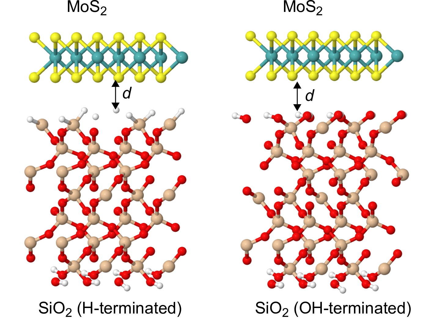
We use the simulation parameters from Table 1 in our calculations. The TMD-substrate gap size is a parameter in a continuum model in which we treat the substrate as a continuous dielectric solid with a well-defined surface at which the dielectric function changes discontinuously from to . However, there is no well-defined, exact point in atomistic models where we can say that the dielectric function changes suddenly. Hence, the precise value of cannot be determined from atomistic models. Moreover, the value of estimated from atomistic models can vary with the chemical configuration of the substrate surface. Thus, given the uncertainty in , we look at the range of values for different values of instead of computing for a single fixed value.
We estimate nm for the TMD-SiO2 interfaces from the position of the highest substrate atom to the lowest TMD atom in the TMD-SiO2 supercells optimized with density functional theory (DFT) calculations, the details of which are given in the Appendix A. We also assume nm for the TMD-HfO2 and TMD-Al2O3 interfaces for convenience. Our calculations are repeated for and nm, because of the strong -dependence from the term in Eq. (9), to set the upper and lower bounds for , respectively.
| Substrate | SiO2 | Al2O3 | HfO2 |
|---|---|---|---|
| (WS2) and (MoS2) | |||
| (WS2 and MoS2) | |||
| (WS2 and MoS2) | |||
| (nm) | (WS2 and MoS2) | ||
| 2.50 | 3.20 | 5.03 | |
| 3.05 | 7.27 | 6.58 | |
| 3.90 | 12.53 | 22.00 | |
| (meV) | 55.60 | 48.18 | 12.40 |
| (meV) | 138.10 | 71.41 | 48.35 |
| (meV) | 60.99 | 56.08 | 21.26 |
| (meV) | 148.97 | 110.11 | 55.08 |
III Numerical results and discussion
To understand the experimental implications of the physics underlying the electronic TBC, we compute the electronic TBC using Eq. (9) for the single-layer TMDs (MoS2 and WS2) and dielectric substrates (SiO2, Al2O3, and HfO2) at different temperatures () and electron densities () since and can be varied in experiments. In field-effect transistors, the electron density is modulated by the gate electrode and can reach up to cm-2 (Yu et al. 2014; Yu et al. 2016). Intuitively, we expect to increase with as more electron-phonon scattering events occur at higher . However, at higher , the mobile electrons can also be polarized by an external electric field and generate a polarization field that attenuates the original external field. This effect is known as screening and it is expected to weaken the effective electron-phonon interaction, possibly offsetting the gain in from the greater frequency of electron-phonon scattering. By studying the dependence of , we clarify these two competing effects on .
III.1 dependence on electron screening
It is shown in Ref. (Ong et al. 2013) that in single-layer graphene can vary substantially depending on the form of the electron-phonon interaction in Eq. (5), with for the bare or unscreened electron-phonon interaction (i.e. the unscreened ) up to two orders of magnitude larger than for the weaker screened electron-phonon interaction (i.e. the screened ). Experimental TBC data from Koh and co-workers for the graphene-SiO2 interface (Koh et al. 2016) suggest that changes in the TBC are only weakly dependent on the electron density , consistent with the screened . On the other hand, theories involving unscreened remote phonon interaction have been used to model heat dissipation in carbon nanotubes (Rotkin et al. 2009). To settle this question for TMDs and to determine the significance of screening for in TMDs, we compute the unscreened and screened using Eq. (9). For screened interactions, we use Eq. (7) while for unscreened interactions, we set in Eq. (9).
Figure 1 shows as a function of at K for the MoS2-SiO2 and WS2-SiO2 interfaces. For the MoS2-SiO2 interface, the unscreened shows an order of magnitude rise from to MW/K/m2 as increases from to cm-2 while the screened increases from to MW/K/m2. This difference in the dependence on illustrates the significance of screening for the TBC. At low where screening is weak, the unscreened and screened values are close but at high , the screening of becomes more significant and the screened diverges from the unscreened . We surmise that the large unscreened increase is unlikely to be correct given the much smaller MoS2-SiO2 TBC observed in Refs. (Yalon et al. 2017a; Yalon et al. 2017b). Thus, electron screening must be taken into consideration in order to model electronic heat transfer at TMD-substrate interfaces. Nonetheless, even with the effects of screening, the dependence of is still significant and should be detectable in a MoS2 or WS2 field-effect transistor on a typical Si/SiO2 substrate.
We observe that is larger for MoS2 than for WS2. At cm-2, the unscreened is and MW/K/m2 for the MoS2-SiO2 and WS2-SiO2 interface, respectively (Ong et al. 2013), i.e., is percent higher for MoS2. This is due to the higher electron density of states for MoS2, which is a constant proportional to the electron effective mass (Davies 1997) and corresponds to a greater amount of scattering. The relative difference is further enhanced for the screened , with the screened for MoS2 about percent higher, indicating that a higher also leads to weaker screening of the electron-phonon interaction. This is because at a higher density of states, the greater availability of states lowers the chemical potential which in turn decreases the screening strength. This combined effect of a lower density of states and stronger screening also explains why is significantly lower for graphene. At cm-2, the unscreened is and MW/K/m2 for the MoS2-SiO2 and graphene-SiO2 interface, respectively (Ong et al. 2013). Unlike the 2DEG in MoS2 or WS2 which has a parabolic dispersion (), the 2DEG in graphene has a linear dispersion () akin to a massless Dirac particle. Thus, the electronic density of states in graphene scales as near the Dirac point, which results in a reduced amount of scattering and stronger screening of the electron-phonon coupling, leading to a smaller .

III.2 dependence on substrate dielectric material, electron density and temperature
Figures 2(a) to 2(f) show the electronic TBC from Eq. (9) as a function of the electron density at K for different substrates (SiO2, HfO2, and Al2O3) and a TMD-substrate distance of nm. The lower and upper bounds for , corresponding to and nm, respectively, are also shown. As noted earlier, increases monotonically from 0 with because of the higher rate of inelastic scattering events at higher . However, the rate of increase of with respect to decreases at higher electron densities because the higher rate of inelastic scattering events is offset partially by the greater electron screening which weakens the electron-phonon coupling. We find that is higher for MoS2 than WS2 with every substrate and that Al2O3 is the substrate with the highest because it has the highest bare electron-phonon coupling strength which we can characterize by the dimensionless parameter (, and for SiO2, HfO2 and Al2O3, respectively). The higher for MoS2 can be explained by its greater electron effective mass which is proportional to the electron density of states (Davies 1997).
By increasing the electron density to cm-2 which can be attained in MoS2 field-effect transistors (Yu et al. 2014; Yu et al. 2016), can reach a maximum of , and MW/K/m2 in Al2O3, HfO2 and SiO2, respectively. This figure represents the gate-tunable component of the overall TBC, which is the sum of and the phononic TBC component, and suggests that the gate-tunable is most pronounced and easily observed for the TMD-Al2O3 interface at room temperature since as theoretical results from Ref. (Foss and Aksamija 2019) estimate that MW/K/m2 for the TMD-Al2O3 interface. This tunability should also be observable for the commonly used SiO2-supported TMD field-effect transistors because classical MD simulation results for the TBC of the MoS2-SiO2 interface ( MW/K/m2 in Ref. (Yasaei et al. 2017), – MW/K/m2 in Ref. (Farahani et al. 2018) and MW/K/m2 in Ref. (Suryavanshi et al. 2019)) suggest that should be in the to MW/K/m2 range at room temperature for the TMD-SiO2 interface, comparable to the change in from to MW/K/m2 when increases from to cm-2. The tunability of also suggests that the gate voltage can be adjusted to modulate cross-plane heat transfer between the TMD and the substrate. One can exploit this effect to create gate-tunable thermal insulators by layering the TMD with other 2D materials (Vaziri et al. 2019) and then using a gate metal electrode to either raise or lower the TBC to facilitate or inhibit heat transfer at the TMD-substrate interface.

Figures 3(a) to 3(f) show the temperature dependence of at cm-2 for nm from to K, a temperature range that is experimentally accessible. We find that increases monotonically with in this temperature range for the TMD-SiO2 and TMD-Al2O3 interfaces because the phonon population increases with . On the other hand, for the TMD-HfO2 interface exhibits a similar trend (i.e., ) initially but plateaus and then starts to decrease with the temperature at higher because the expression in Eq. (10) scales as at higher (i.e., ) given the relatively small SO1 phonon frequency ( meV) in HfO2. This difference in the behavior of the temperature dependence of for different substrates can be used to distinguish the effects of the electronic TBC. With Al2O3 as the substrate, we predict that the TBC contribution from is not only large (relative to the other substrates), but is expected to have a pronounced temperature dependence that can be verified in experiments, while with HfO2, the temperature dependence is predicted to be significantly weaker. The distinct temperature dependence of HfO2 and Al2O3 suggests that different substrate materials can be used for heat-transfer applications at different temperature regimes. HfO2 can be used at low temperatures ( K) while Al2O3 can be used at higher temperatures ( K).

IV Summary and conclusion
In this work, we have developed a theoretical model of electronic thermal boundary conductance (TBC) via the remote phonon scattering of electrons in single-layer MoS2 and WS2 supported on dielectric substrates. We have verified that screened electron-phonon interactions are necessary for realistic predictions. Our model predicts that the electronic TBC is highly dependent on the electron density and is strongly tunable using the gate electrode in field-effect transistors, with the strongest effect seen for Al2O3. We have also identified the temperature dependence of the electronic TBC for each dielectric substrate and the temperature regimes at which each substrate material is more effective in interfacial heat transfer. This strong dependence of the electronic TBC on the electron density can be exploited for the design of novel thermal devices with gate voltage-modulated cross-plane heat dissipative properties.
Appendix A Estimation of TMD-SiO2 gap
The gap size () of the TMD-SiO2 interface can be estimated from the distance between the highest substrate atom and the lowest TMD atom. The WS2-SiO2 and MoS2-SiO2 heterostructures are optimized structurally within the framework of density functional theory (DFT) using the software package VASP (Kresse and Furthmüller 1996). The DFT-D2 method is adopted to simulate the van der Waals interactions across the interface while the Perdew-Burke-Ernzerhof functional is used as the exchange correlation functional together with a cutoff energy of 400 eV. The slab models of the heterostructures are constructed with a vacuum layer thicker than 10 Å. For the TMD-SiO2 interface, the heterostructures are constructed from a supercell for the TMD (MoS2 or WS2) and a supercell for the SiO2 (001) surface to ensure a better lattice match with lattice strains smaller than 2 percent. To simulate the SiO2 substrate, a slab model with seven Si layers is used and the atoms in the bottom O-Si-O atomic layers are saturated with hydrogen atoms and fixed during structural optimization. We adopt a Monkhorst-Pack (MP) grid for k-point sampling for the TMD-SiO2 heterostructures. All the atomic models are fully relaxed until the forces are smaller than 0.005 eV/Å.
Figure 4 shows the MoS2-SiO2 heterostructures for different SiO2 surface configurations (H-terminated and OH-terminated), similar to those used in Ref. (Ong et al. 2016). We estimate and nm for the H-terminated and OH-terminated SiO2 surface, respectively. This shows that the estimate of can vary with the chemical structure of the substrate surface. Hence, it is simpler to approximate nm for the MoS2-SiO2 interface. Our calculations repeated for the different WS2-SiO2 interfacial configurations like in Fig. 4 also suggest that nm for the WS2-SiO2 interface.
Acknowledgements.
The authors gratefully acknowledge support from the Science and Engineering Research Council through Grant No. 152-70-00017 and the use of computing resources at the A*STAR Computational Resource Centre and National Supercomputer Centre, Singapore. We also thank Yongqing Cai (University of Macau) for assistance with the DFT calculations.References
- Li et al. (2015) X. Li, L. Yang, M. Si, S. Li, M. Huang, P. Ye, and Y. Wu, Advanced Materials 27, 1547 (2015).
- Lembke et al. (2015) D. Lembke, S. Bertolazzi, and A. Kis, Accounts of Chemical Research 48, 100 (2015).
- Pop (2010) E. Pop, Nano Research 3, 147 (2010).
- Ong and Bae (2019) Z.-Y. Ong and M.-H. Bae, 2D Materials 6, 32005 (2019).
- Ong et al. (2018) Z.-Y. Ong, B. Qiu, S. Xu, X. Ruan, and E. Pop, J. Appl. Phys. 123, 115107 (2018).
- Suryavanshi et al. (2019) S. V. Suryavanshi, A. J. Gabourie, A. Barati Farimani, and E. Pop, J. Appl. Phys. 126, 55107 (2019).
- Persson et al. (2011) B. N. J. Persson, A. I. Volokitin, and H. Ueba, J. Phys.: Condens. Matter 23, 45009 (2011).
- Ong et al. (2016) Z.-Y. Ong, Y. Cai, and G. Zhang, Phys. Rev. B 94, 165427 (2016).
- Ong (2017) Z.-Y. Ong, Phys. Rev. B 95, 155309 (2017).
- Correa et al. (2017) G. C. Correa, C. J. Foss, and Z. Aksamija, Nanotechnology 28, 135402 (2017).
- Hess and Vogl (1979) K. Hess and P. Vogl, Solid State Communications 30, 797 (1979).
- Fischetti et al. (2001) M. V. Fischetti, D. A. Neumayer, and E. A. Cartier, J. Appl. Phys. 90, 4587 (2001).
- Konar et al. (2010) A. Konar, T. Fang, and D. Jena, Phys. Rev. B 82, 115452 (2010).
- Zou et al. (2010) K. Zou, X. Hong, D. Keefer, and J. Zhu, Phys. Rev. Lett. 105, 126601 (2010).
- Yu et al. (2016) Z. Yu, Z.-Y. Ong, Y. Pan, Y. Cui, R. Xin, Y. Shi, B. Wang, Y. Wu, T. Chen, Y.-W. Zhang, G. Zhang, and X. Wang, Advanced Materials 28, 547 (2016).
- Ong et al. (2013) Z.-Y. Ong, M. V. Fischetti, A. Y. Serov, and E. Pop, Phys. Rev. B 87, 195404 (2013).
- Yu et al. (2014) Z. Yu, Y. Pan, Y. Shen, Z. Wang, Z. Y. Ong, T. Xu, R. Xin, L. Pan, B. Wang, L. Sun, J. Wang, G. Zhang, Y. W. Zhang, Y. Shi, and X. Wang, Nature Communications 5, 5290 (2014).
- Taube et al. (2015) A. Taube, J. Judek, A. Lapinska, and M. Zdrojek, ACS Appl. Mater. Interfaces 7, 5061 (2015).
- Yalon et al. (2017a) E. Yalon, C. J. McClellan, K. K. H. Smithe, M. Munoz Rojo, R. L. Xu, S. V. Suryavanshi, A. J. Gabourie, C. M. Neumann, F. Xiong, A. B. Farimani, and E. Pop, Nano Letters 17, 3429 (2017a).
- Yalon et al. (2017b) E. Yalon, O. B. Aslan, K. K. H. Smithe, C. J. McClellan, S. V. Suryavanshi, F. Xiong, A. Sood, C. M. Neumann, X. Xu, K. E. Goodson, T. F. Heinz, and E. Pop, ACS Appl. Mater. Interfaces 9, 43013 (2017b).
- Yasaei et al. (2017) P. Yasaei, C. J. Foss, K. Karis, A. Behranginia, A. I. El-Ghandour, A. Fathizadeh, J. Olivares, A. K. Majee, C. D. Foster, F. Khalili-Araghi, Z. Aksamija, and A. Salehi-Khojin, Advanced Materials Interfaces 4, 1700334 (2017).
- Koh et al. (2016) Y. K. Koh, A. S. Lyons, M. H. Bae, B. Huang, V. E. Dorgan, D. G. Cahill, and E. Pop, Nano Lett. 16, 6014 (2016), arXiv:1603.00358 .
- Mahan (2000) G. D. Mahan, Many-Particle Physics (Springer-Verlag, Boston, MA, 2000).
- Maldague (1978) P. F. Maldague, Surface Science 73, 296 (1978).
- Ong and Fischetti (2012a) Z.-Y. Ong and M. V. Fischetti, Phys. Rev. B 86, 121409 (2012a).
- Jin et al. (2014) Z. Jin, X. Li, J. T. Mullen, and K. W. Kim, Phys. Rev. B 90, 045422 (2014), arXiv:1406.4569 .
- Ong and Fischetti (2012b) Z.-Y. Ong and M. V. Fischetti, Phys. Rev. B 86, 165422 (2012b).
- Rotkin et al. (2009) S. V. Rotkin, V. Perebeinos, A. G. Petrov, and P. Avouris, Nano Lett. 9, 1850 (2009).
- Davies (1997) J. H. Davies, The Physics of Low-dimensional Semiconductors (Cambridge University Press; 1 edition, New York, 1997).
- Foss and Aksamija (2019) C. J. Foss and Z. Aksamija, 2D Materials 6, 025019 (2019).
- Farahani et al. (2018) H. Farahani, A. Rajabpour, M. Khanaki, and A. Reyhani, Computational Materials Science 142, 1 (2018).
- Vaziri et al. (2019) S. Vaziri, E. Yalon, M. M. Rojo, S. V. Suryavanshi, H. Zhang, C. J. McClellan, C. S. Bailey, K. K. Smithe, A. J. Gabourie, V. Chen, S. Deshmukh, L. Bendersky, A. V. Davydov, and E. Pop, Science Advances 5, 1325 (2019).
- Kresse and Furthmüller (1996) G. Kresse and J. Furthmüller, Phys. Rev. B 54, 11169 (1996).
- (34) “Jmol: An open-source JAVA viewer for chemical structures in 3D.” .