See Titlepage.pdf
Technical design of the phase I Mu3e experiment
K. Arndt†a, H. Augustinb, P. Baessoc, N. Bergerd, F. Berge, C. Betancourtf, D. Bortolettoa, A. Bravarg, K. Brigglg,11 1 Now at Kirchhoff-Institut, Universität Heidelberg, D. vom Bruchd,22 2 Now at Université de Marseille, France, A. Buonaurae, F. Cadouxg, C. Chavez Barajash, H. Cheni, K. Clarkc, P. Cookeh, S. Corrodie,33 3 Now at Argonne National Laboratory, Lemont, IL, USA, A. Damyanovag, Y. Demetsg, S. Dittmeierb, P. Eckerti, F. Ehrlerj, D. Fahrnik, S. Gagneurd, L. Gerritzene, J. Goldsteinc, D. Gottschalkb, C. Grabe, R. Gredigf, A. Grovesh, J. Hammerichb,44 4 Now at University of Liverpool, UK, U. Hartensteind, U. Hartmannk, H. Haywardh, A. Herkertb,55 5 Now at DESY, Hamburg, Germany, G. Heskethl, S. Hetzelb, M. Hildebrandtk, Z. Hodgek,66 6 Now at University of Washington, Seattle, WA, USA, A. Hoferk, Q.H. Huangd,77 7 Now at Institut Polytechnique de Paris, France, S. Hughesh, L. Huthb,88 8 Now at DESY, Hamburg, Germany, D.M. Immigb, T. Jonesh, M. Jonesa, H.-C. Kästlik, M. Köppeld, P.-R. Kettlek, M. Kiehnb,99 9 Now at CERN, Genève, Switzerland, S. Kilanil, H. Klingenmeyeri, A. Knechtk, A. Knighta, B. Kotlinskik, A. Kozlinskiyd, R. Leysj, G. Lockwooda, A. Loretia,1010 10 Also at University of Bristol, UK, D. La Marrag, M. Müllerd, B. Meierk, F. Meier Aeschbacherk,, A. Menesesb, K. Metodieva, A. Mtchedlishvilik, S. Muleyb, Y. Munwesi, L.O.S. Noehteb,1111 11 Now at University of Zürich and Paul Scherrer Institut, Switzerland, P. Owenf, A. Papak,1212 12 Also at University of Pisa, Department of Physics and INFN, Italy, I. Paraskevasl, I. Perićj, A.-K. Perrevoortb,1313 13 Now at NIKHEF, Amsterdam, The Netherlands, R. Placketta, M. Pohlg, S. Rittk, P. Robmannf, N. Rompotish, T. Rudzkib, G. Rutark, A. Schöningb, R. Schimassekj, H.-C. Schultz-Couloni, N. Serraf, W. Sheni, I. Shipseya, S. Shresthab,1414 14 Now at Arcadia University, Glenside, PA, USA, O. Steinkampf, A. Stoykovk, U. Straumannf, S. Streulik, K. Stumpfb, N. Tataa,1515 15 Now at Harvard University, Cambridge, MA, USA, J. Velthuisc, L. Viganib, E. Vilella-Figuerash, J. Vossebeldh, R. Wallnye, A. Wasilih, F. Wautersd, A. Weberbj, D. Wiednerb,1616 16 Now at Technische Universität Dortmund, Germany, B. Windelbandb, T. Zhongi
aDepartment of Physics, University of Oxford, Denys Wilkinson Building, Keble Road, Oxford OX1 3RH, United Kingdom
bPhysikalisches Institut, Universität Heidelberg, Im Neuenheimer Feld 226, 69120 Heidelberg, Germany
cUniversity of Bristol, H.H. Wills Physics Laboratory, Tyndall Avenue, Bristol BS8 1TL, United Kingdom
dInstitut für Kernphysik und Exzellenzcluster PRISMA+, Johannes Gutenberg-Universität Mainz, Johann-Joachim-Becher-Weg 45, 55128 Mainz, Germany
eInstitute for Particle Physics and Astrophysics, Eidgenössische Technische Hochschule Zürich, Otto-Stern-Weg 5, 8093 Zürich, Switzerland
fPhysik-Institut, Universität Zürich, Winterthurerstrasse 190, 8057 Zürich, Switzerland
gDépartement de physique nucléaire et corpusculaire, Université de Genève, 24, quai Ernest-Ansermet, 1211 Genève 4, Switzerland
hDepartment of Physics, University of Liverpool, The Oliver Lodge Laboratory, Liverpool L69 7ZE, United Kingdom
iKirchhoff-Institut für Physik, Universität Heidelberg, Im Neuenheimer Feld 227, 69120 Heidelberg, Germany
jInstitut für Prozessdatenverarbeitung und Elektronik, Karlsruhe Institut für Technologie, Hermann-von-Helmholtz-Platz 1, 76344 Eggenstein-Leopoldshafen, Germany
kLaboratory for Particle Physics, Paul Scherrer Institut, Forschungsstrasse 111, 5232 Villigen, Switzerland
lDepartment of Physics and Astronomy, University College London, Gower Street, London WC1E 6BT, United Kingdom
Abstract
The Mu3e experiment aims to find or exclude the lepton flavour violating decay at branching fractions above . A first phase of the experiment using an existing beamline at the Paul Scherrer Institute (PSI) is designed to reach a single event sensitivity of . We present an overview of all aspects of the technical design and expected performance of the phase I Mu3e detector. The high rate of up to muon decays per second and the low momenta of the decay electrons and positrons pose a unique set of challenges, which we tackle using an ultra thin tracking detector based on high-voltage monolithic active pixel sensors combined with scintillating fibres and tiles for precise timing measurements.
Spokespersons: S. Ritt (stefan.ritt@psi.ch), A. Schöning (schoning@physi.uni-heidelberg.de)
Technical coordinator and editor: F. Meier Aeschbacher (frank.meier@psi.ch),
Kirk Arndt
Silicon Detector Development Engineer (1959-2019)
Kirk Arndt was a silicon detector development engineer. He came to Europe in 2014 after an illustrious career in the U.S. where he became known as “the best pair of hands in the silicon business”. He built some remarkable silicon digital cameras for particle physics at the University of California Santa Barbara, Purdue University, and Oxford including one that glimpsed the Higgs particle for the first time at the LHC at CERN in 2012. These were the Silicon Micro-Vertex Detector for the CLEO II.V experiment at the Cornell Electron Storage Ring with UCSB, the CLEO III Silicon Vertex Detector and the CMS Phase 0 and Phase 1 Silicon Forward Pixel Detectors for the CMS experiment at the LHC at CERN with Purdue, and he was working on the ATLAS Upgrade Silicon Forward Pixel Detector at Oxford, the Mu3e tracker and detectors for photon science at the time of his death. For over a decade he also played an important role in the design of the 3.2 Gigapixel camera for the Large Synoptic Survey Telescope both at Purdue and Oxford.
Kirk was a very highly valued and widely appreciated colleague. He was always ready to help colleagues in the CLEO, CMS, LSST, ATLAS and Mu3e collaborations and many others in the international community who sought him out for advice. His positive can do attitude, exacting professional standards, dedication, willingness to nurture younger colleagues and his kindness are an example to us all. Shortly before his unexpected death at the age of 59, he hosted a Mu3e collaboration meeting in Oxford. It was a privilege to work with Kirk. He will live on in the hearts and minds of all that knew him.
Chapter 0 The Decay and the Experimental Challenge
1 Goals of the Experiment
The goal of the Mu3e experiment is to observe the process 1717 17 We will refer to this decay as in this document; the charge of the muon is always positive. if its branching fraction is larger than , or otherwise to exclude a branching fraction of at the confidence level. In order to achieve these goals, more than muons have to be stopped in the detector (assuming a total reconstruction efficiency of ) and any background mimicking the signal process suppressed to below the level. The additional requirement of achieving these goals within a reasonable measurement time of one year of data taking dictates a muon stopping rate of , along with a high geometrical acceptance and efficiency for the experiment.
The current best source of low-energy muons in the world, the E5 beam line at PSI, provides muon rates up to . Higher intensities are possible and currently under study in the high intensity muon beam (HiMB) project. However, the new beamlines will not be available before 2025. In order to establish the novel technologies for Mu3e, set first competitive limits and prepare for the very high intensity running, we plan to run a phase I experiment at E5. The aim of this phase I experiment is a single event sensitivity of on the branching fraction, which would require stopped muons1818 18 for a sensitivity and a total efficiency (phase I) or (290 days) of run time at stopping rate. The present document describes the technical design of this phase I detector.
For more on the physics motivation and theory predictions, please consult the Mu3e letter of intent [1] and research proposal [2]. This chapter describes the kinematics of the signal and the main background sources, and how these motivate the design of the experiment. Running with of muon decays also poses challenges for the detectors, the data acquisition and the readout, which will be discusses in later chapters.
2 Signal Kinematics
To discriminate the signal from the background, energy and momentum conservation are exploited. The decaying muons are at rest and the three decay particles are emitted at the same time. The vectorial sum of all decay particle momenta should therefore vanish:
| (1) |
and the invariant mass, which is equal to the sum of the energies in the case of vanishing momentum, be equal to the muon mass:
| (2) |
The energies of the decay particles range from the electron mass up to half the muon mass, which is about . All decay particles must lie in a plane. Therefore, the decay is described by two independent variables in addition to three global rotation angles describing the orientation in space.
3 Modelling of the Signal
The decay dynamics for the signal are dependent on the unknown lepton flavour violating (LFV) mechanism. We typically assume a phase-space distribution for the signal electrons in our simulations, if not stated otherwise. In order to study effects of different decay dynamics, we utilise the general parametrised Lagrangian proposed by Kuno and Okada [3]:
| (3) |
The form factors describe tensor type (dipole) couplings, mostly acquiring contributions from the photon penguin diagram, whereas the scalar-type () and vector-type () form factors can be regarded as four fermion contact interactions, to which the tree diagram contributes at leading order. We generate different signal models by varying the relative strengths of the and parameters.
4 Signal Acceptance
For a three-body decay with a priori unknown kinematics such as , the acceptance has to be as high as possible in order to test new physics in all regions of phase space. To illustrate the phase space coverage needed, the energy spectrum of the highest energy decay particle () for various LFV coupling amplitudes is shown in Figure 1, and the fraction of events where all decay particles have transverse momenta above is shown in Figure 2. From these figures, it can be seen that a high acceptance for the signal is only possible if the detector can reconstruct tracks with momenta ranging from half the muon mass down to a few . This must be achieved with large solid angle coverage, limited by the beam entry and exit points preventing instrumentation.
5 Backgrounds
The Standard Model branching fraction for the process is (normal neutrino mass ordering) or (inverted ordering) [5, 6]; the experiment therefore has no irreducible physics backgrounds, and the final sensitivity depends purely on the ability to reduce backgrounds in two categories: overlays of different processes producing three tracks resembling a decay (combinatorial background) and radiative decays with internal conversion (internal conversion background) with a small energy fraction carried away by the neutrinos; see Figure 3 for the signal and background topologies. Combinatorial backgrounds have to be suppressed via vertexing, timing and momentum measurement; momentum measurement is the only handle on internal conversion. In the following sections, these main background sources are discussed.
1 Internal Conversions
The decay occurs with a branching fraction of [7]. It can be distinguished from the process by making use of energy and momentum conservation to infer the presence of the undetected neutrinos: in order to separate the events from events, the total momentum in the event is required to be zero and the visible mass (defined as the invariant mass of the three electrons) equal to the muon rest energy. The branching fraction for [4] decays above a given visible mass value is shown in Figure 4. s 5 and 6 show the energy spectrum of all and the lowest energy electron from decays calculated with the matrix element from [4]. Recently, next-to-leading order (NLO) calculations of the internal conversion decays have become available [8, 9]; they predict branching fractions close to the end-point that are about smaller than the leading order (LO) prediction.
Internal conversion is the most serious background for the search, and the momentum resolution directly determines to what level it can be suppressed and thus the experiment run background free. In order to reach a sensitivity of with a cut on the reconstructed muon mass, the average three-particle mass resolution has to be better than , see Figure 7, and is not allowed to have sizeable tails towards the high momentum side.
2 Combinatorial Backgrounds
Michel Decays
Using a beam of positive muons, one of the main processes contributing to combinatorial background is that of the Michel decay . This process does not produce a negatively charged particle (electron), so it can only contribute as a background in combination with an incorrectly reconstructed track, or with other processes that “naturally” provide negatively charged particles.
The rate of fake electron tracks being reconstructed from those positrons performing complete turns in the magnetic field is reduced by a reliable determination of the direction of motion of particles: achieved by accurate curvature measurements and accurate time of flight measurements. The main sources of genuine negatively charged particles are Bhabha scattering and radiative decays.
Radiative Muon Decays
The process (branching fraction for photon energies above [10]) can deliver a negatively charged electron if the photon converts either in the target region or in the detector. Conversions in the target region generate an event topology similar to the radiative decay with internal conversion discussed above. Contributions from conversions outside the target region are greatly suppressed both by a vertex constraint and by minimising the material in both the target and detector. However, this process can still contribute to the combinatorial background in combination with an ordinary muon decay.
As for the internal conversion background, a NLO calculation for radiative decay has recently been published [11] and is implemented in the Mu3e simulation.
Bhabha Scattering
Any positron, either from a muon decay in the target or in the beam, can undergo Bhabha scattering with electrons in the target material, leading to an electron-positron pair from a common vertex. In combination with a positron from a Michel decay, this can mimic a signal decay. In addition, Bhabha scattering is the main source of electrons for combinatorial background involving two Michel decays. Similarly to the external photon conversion background, the amount of Bhabha scattering is reduced by minimising both the amount, and the average atomic number of the material in the target.
Vertex and Timing Resolution Requirements
Separating vertices from different muon decays is a key tool in suppressing combinatorial background. The vertex position resolution is essentially determined by the amount of multiple scattering (and thus material) in the innermost detector layer and the stopping target as well as the average distance between the vertex and the first detector layer.
At high muon rates, good time resolution is essential for reducing combinatorial background, while also facilitating event reconstruction. The combinatorial background has a component scaling linearly with the rate ( pair plus a Michel positron) and a component quadratic in the rate (electron plus two Michel positrons). The suppression of these components by timing measurements is also linear and quadratic in the timing resolution. Simulation studies have shown that the linear part dominates at rates at least up to muon stops per second. The requirement of reducing the combinatorial background by at least two orders of magnitude puts very tight demands on the resolution of the timing detectors. The timing resolution should be below per track to allow for reliable charge identification by time-of-flight and ideally or better to identify non-synchronous muon decays.
3 Other Backgrounds
Pion Decay
Certain pion decays, especially (branching fraction [12]) and (branching fraction [13]) with subsequent photon conversion are indistinguishable from signal events if the momenta of the final state particles fit the muon mass hypothesis. The low pion contamination in the muon beam delivered to the experiment ( of the muon flux), in addition to the small branching fractions, lead to negligible rates for these backgrounds.
Mis-reconstruction
Mis-reconstruction of tracks (e.g. from hits created by different particles or noise hits) combined with real tracks from muon decays can fake decays. Great care is taken in the track reconstruction algorithms to keep a minimal rate of fake tracks, balanced against reconstruction efficiency.
4 Summary
The sensitivity aims of the Mu3e experiment place strict requirements on the experimental design. Electrons and positrons must be reconstructed down to a few with large solid angle coverage, running at a rate of of muon decays. The material in the target and detector must be minimised, while achieving excellent momentum, vertex and timing resolution to suppress backgrounds to the necessary level. The following chapters will provide a description of the experimental apparatus and procedures that will allow this is to be achieved.
Chapter 1 Experimental Concept
Phase I of the Mu3e experiment aims for the background free measurement or exclusion of the branching fraction for the decay at the level of . As discussed in more detail in id1, these goals require running at high muon rates, excellent momentum resolution to suppress background from internal conversion decay (), and a good vertex and timing resolution to suppress combinatorial background. The present chapter introduces the conceptual design of the Mu3e experiment, driven by these requirements.
The momenta of electrons and positrons from muon decays are measured using a silicon pixel tracker in a solenoidal magnetic field. At the energies of interest, multiple Coulomb scattering in detector material is the dominating factor affecting the momentum resolution. Minimising the material in the detector is thus of the utmost importance.
The detector consists of an ultra-thin silicon pixel tracker, made possible by the High-Voltage Monolithic Active Pixel (HV-MAPS) technology (see chapter 6). Just four radial layers of HV-MAPS sensors around a fixed target in a solenoidal magnetic field allow for precise momentum and vertex determination. Two timing detector systems guarantee good combinatorial background suppression and high rate capabilities.
1 Momentum Measurement with Recurlers
With a fine-grained pixel detector, we are in a regime where multiple scattering effects dominate over sensor resolution effects, see s 1 and 2. Adding additional measurement points does not necessarily improve the precision.
The precision of a momentum measurement depends on the amount of track curvature in the magnetic field and the multiple scattering angle , see Figure 3; to first order:
| (1) |
So in order to have a high momentum precision, a large lever arm is needed. This can be achieved by moving tracking stations to large radii, which would limit the acceptance for low momentum particles. Instead, we utilise the fact that, in the case of muon decays at rest, all track momenta are below and all tracks will curl back towards the magnet axis if the magnet bore is sufficiently large. After half a turn, effects of multiple scattering on the momentum measurement cancel to first order, see Figure 4. To exploit this feature, the experimental design is optimised specifically for the measurement of recurling tracks, leading to a narrow long tube layout.
Determining the momentum from a particle’s trajectory outside the tracker allows us to place thicker timing detectors on the inside both upstream and downstream of the target without significantly affecting the resolution, see Figure 6.
2 Coordinate System
The Mu3e coordinate system is centred in the muon stopping target with the axis pointing in beam direction, the axis pointing upward and the axis chosen to obtain a right handed coordinate system. The polar angle measured from the axis is denoted with , and measured from the - plane denoted with . Azimuthal angles are denoted with .
3 Baseline Design
The proposed Mu3e detector is based on two double-layers of HV-MAPS around a hollow double cone target, see s 6 and 5. The outer two pixel sensor layers are extended upstream and downstream to provide precise momentum measurements in an extended region to increase the acceptance for recurling electrons and positrons. The silicon detector layers (described in detail in chapter 6) are supplemented by two timing systems, a scintillating fibre tracker in the central part (see chapter 9) and scintillating tiles (chapter 10) inside the recurl layers. Precise timing of all tracks is necessary for event building and to suppress the combinatorial background.
4 Detector Readout
The Mu3e experiment will run a continuous, triggerless readout, and employs application-specific integrated circuits (ASICs) for the pixel and timing detectors which stream out zero-suppressed digital hit data. These hits are collected by field-programmable gate arrays (FPGAs) located on front-end boards and then optically forwarded to switching boards, which in turn distribute them to a computer farm. This network makes it possible for every node in the farm to have the complete detector information for a given time slice. Decays are reconstructed using graphics processing units, and interesting events are selected for storage. A system overview is shown in Figure 8 and a detailed description can be found in chapter 16.
5 Building up the Experiment
One of the advantages of the design concept presented is its modularity. Even with a partial detector, physics runs can be taken. In an early commissioning phase at smaller muon stopping rates, the detector will run with all of the timing detectors but only the central barrel of silicon detectors. The silicon detectors of the recurl stations are essentially copies of the central outer silicon detector; after a successful commissioning of the latter, they can be produced and added to the experiment as they become available. The configuration with two recurl stations (s 6 and 5) defines a medium-size setup, well suited for phase I running at the highest possible rate at the E5 muon beam line at PSI of . The sensitivity reach in this phase of the experiment of will be limited by the available muon rate.
6 The Phase II Experiment
A new high intensity muon beam line, delivering muons and currently under study at PSI, is crucial for Mu3e phase II. To fully exploit the new beam facility the detector acceptance of phase I will be further enhanced by longer detector stations, see Figure 7. These longer stations will allow the precise measurement of the momentum of all particles in the acceptance of the inner tracking detector. At the same time the longer tile detector stations with their excellent time resolution and small occupancy will help to fight the increased combinatorial backgrounds at very high decay rates. The larger initial muon rate allows for a more restrictive collimation of the beam and thus a smaller (and potentially longer) target region leading to a much improved vertex resolution. The HV-MAPS technology can reach a time resolution of if an adequate time-walk correction is implemented – this would allow to further reduce combinatorial background without adding material and could eventually replace the scintillating fibre detector. Advanced wafer post-processing technologies and chip-to-chip bonding could obviate the need for parts of the flexprints, further reducing the multiple scattering. The combined performance of the enhanced detector setup together with the high stopping rate will allow to search for the decay with a sensitivity of B(). Whilst we always keep this ultimate goal in mind, the rest of this document is concerned with the phase I detector for existing beamlines.
Chapter 2 Muon Beam
1 Beam Requirements
An experiment such as Mu3e, with a phase I sensitivity goal of while challenged by combinatorial background, not only requires running at the intensity frontier, but also substantially benefits from a continuous beam structure rather than a pulsed one, allowing a lower instantaneous muon rate. Both of these conditions are satisfied by the high intensity proton accelerator complex (HIPA) at PSI running at of beam power.
Mu3e requires a muon beam with the highest possible rate of “surface muons”, produced from stopped pion decay at the surface of the primary production target [14]. The surface muon yield and hence beam intensity peaks at around , close to the kinematic edge of the two-body momentum spectrum of pion decay at rest as can be seen from the measured momentum spectrum in Figure 1.
The intensity goal and low energy not only necessitates a beam line capable of guiding these muons to a small, thin stopping target with minimal losses but at the same time minimising beam-related backgrounds. The former requires a small beam emittance and a moderate momentum-byte (full width at half maximum of the momentum acceptance ), with an achromatic final focus to balance between beam intensity and stopping density in the target. The minimising of beam-related backgrounds, in the form of Michel from -decay, produced from -decays in the production target, or from decay-in-flight particles produced along the beam line, puts strong restrictions on the amount of material, such as windows and momentum moderators, that can be placed along the beam path, requiring an extension of the vacuum system to just in front of the target.

2 The Compact Muon Beam Line (CMBL)
For Mu3e phase I, muon intensities close to 108 muons/s will be required, which leaves only one choice of facility in the world, PSI’s E5 channel. This channel will be shared with the upgrade version of the MEG experiment – MEG II [15], whose large detector and infrastructure are permanently located in the rear-part of the E5 area.
The new CMBL for Mu3e, as presented in the following, not only allows the long Mu3e solenoid to be placed in the front part of the E5 area – see Figure 2 – but also allows both experiments MEG II and Mu3e to share the front beam transport elements required by both. This solution allows the efficient switching between experiments by only replacing the superconducting beam transport solenoid of MEG II by a dipole magnet (ASL) for Mu3e.
The initial optical design of the CMBL was modelled using the beam optics matrix code programs graphic transport framework [16] and graphic turtle framework [17], while the detailed modelling was undertaken using the newer geant4 based simulation software g4beamline (g4bl) [18]. The 1st-order optical design showing the vertical and horizontal beam envelopes from Target E to the downstream end of the Mu3e detector are shown in Figure 3.


The design includes the elements of the backward (165∘) extraction channel E5 from Target E up to the ASC dipole magnet, the background cleaning-stage including triplet I, the Wien-filter (SEP41), triplet II and the collimator system, used to eliminate the beam-related background. The final injection stage is based on a very compact “split triplet” layout which starts after the 90∘ dipole ASL41. The “split triplet” consists of the quadrupole doublet QSO41/42 and quadrupole singlet QSM41. In combination with the vertical edge-focusing of the ASK41 65∘ dipole magnet they serve the same purpose as a total of six quadrupoles that would be needed in a more standard beamline configuration. This allows sufficient space to place the long Mu3e detector in the front area without compromising the optics and physics goals of the experiment.
Based on the graphic transport model, two g4bl models were constructed, one including the full E5 channel and Target E, simulating the whole pion production process by protons in the primary target, followed by surface muon production and transport to the intermediate collimator. The second shorter version starts from Triplet II, just upstream of the intermediate focus at the collimator system, where measured phase space parameters determine the initial beam used for the simulation - see Figure 4. The shorter version predictions were used as a direct comparison to the CMBL commissioning measurements described in the next section.
3 CMBL Commissioning Steps
Initial commissioning of the CMBL beam layout was undertaken in two 4-week beam periods in November and December 2014 and May 2015, using mostly existing elements. Figure 5 shows the good agreement between predicted and measured beam sizes at the injection point to the Mu3e solenoid, based on a 1st-order transverse phase space reconstruction. The validated g4bl model was then used, and identified the ASL and ASK dipole apertures as the main limitations for the transmission to the final focus. Consequently, increased pole-gaps and modified vacuum chambers for both dipole magnets allowed for an expected enhanced transmission of 18%, which was proven in the following 2016 measurements [19].

In 2017, the commissioning emphasis was placed on confirmation of increased muon yield using a long production Target E instead of the usual version. The expectation of only an 30% increase in muon yield (surface phenomenon) with a full 50% increase in beam positron contamination (bulk phenomenon) for the 165∘ backward extraction was confirmed. Furthermore, the expected impact on the experiment from an increased beam positron background was also studied and a differential measurement technique developed to distinguish Michel positrons from beam positrons at the final focus [20]. These measurements showed that for the Target E a beam-/-ratio = 10.1 was measured, with no Wien-filter in operation, whereas for a target the ratio was 7. However, with the Wien-filter on, an unacceptably high number of beam positrons, seen as a vertically displaced spot, were measured. On investigation it was found that the off-centre, vertically displaced (by the Wien-filter) beam positrons entering triplet II are partially swept-back into the acceptance of the downstream collimator, as demonstrated in Figure 6. The situation was quickly and temporarily solved by placing a lead -stopper between QSK41/42 reducing the contamination by a factor of 15, with a 10% loss of muons. The final solution is the modification of the Wien-filter, which was upgraded in 2019 to have a symmetric electric field with double the present voltage of . While not yet experimentally confirmed, this is expected to reduce any beam positron contamination by 3-orders of magnitude.

Finally, using the measured contamination rate, the impact of this on the experiment’s sensitivity to combinatorial Michel and beam positron events mimicking a 3-particle signature via Bhabha scattering was investigated [20] and found that only muon decay-in-flight events have a chance of coming close to the reconstructed muon mass region, though occurring at a rate twelve orders of magnitude lower than the most dominant background (Bhabha scattering with overlapping Michel decays).
During the shutdown 2017/18 all magnet power supplies for E5 were replaced with digitally controlled ones. The better stabilisation of magnet currents contributed to a further increased transmission during the 2018 commissioning run. Optimisation at the injection point of the Mu3e solenoid yielded a final rate of /s, normalised to the expected future proton beam current of for a long Target E, with profile widths of = , = , and a momentum-byte of 8%. The measured high (muons only) and low threshold (muons + Michels) profiles are shown in Figure 7, these raster scan profiles were measured with a 2D automated pill scintillator scanner system with each profile consisting of 1025 single measurements. The beam intensity is extracted from a 2D Gaussian fit to the profiles.
The 2018 measurements therefore successfully conclude the beam commissioning up to the injection point of the Mu3e solenoid. The final commissioning to the centre of the Mu3e detector will be undertaken when the magnet is placed in the area.


4 Expected Muon Rate and Distribution on the Mu3e Stopping Target
As described in the previous section the final optimisation of the CMBL resulted in a surface muon rate at the injection point of the Mu3e magnet of /s, normalised to the expected future proton beam current of for a long Target E, with profile widths of = , = , and a momentum-byte of 8%.
The coupling to the central detector region inside the solenoid magnet is planned to be with a custom bellows system (see Figure 5) reducing step-wise the aperture to an inner diameter of for the inner vacuum-pipe. This will contain a thick Mylar (biaxially-oriented polyethylene terephthalate) moderator located at an intermediate focus point some few hundred millimetres in front of the target and will end with a Mylar vacuum window, placed just in front of the Mu3e target, where the aperture narrows down to 40 mm diameter due to the support structure of the inner pixel layers. A double-cone Mylar target of radius , length and total thickness of (see chapter 5) is located close to the vacuum window at the centre of the solenoid. The warm bore of the solenoid is filled with helium gas at atmospheric pressure to reduce multiple scattering. Furthermore, a thick lead collimator system will be introduced shortly after the moderator to protect the inner pixel layers from hits by the muon beam as well as from particles outside of the target acceptance.

Estimates for the final muon stopping rate on the target are based on the re-measured 1- beam emittances at the intermediate collimator system in 2018, corresponding to = , = and the g4bl simulation. The beam losses along the beam line can be seen in Figure 8 and the corresponding beam envelope sizes in Figure 9.
Even though the muon beam intensity at injection into the solenoid achieves the commissioning goal, it is the inner silicon detector diameters and the associated beam pipe size that determine the stopping target diameter, which has been maximised to a radius of . These conditions are a compromise between stopping rate, occupancy and vertex resolution.
The main losses are associated with the transition to the initial diameter of the beam pipe, and the final narrowing to a diameter at its end. The final beam-spot at the target is shown in Figure 10. The beam intensity on the target is expected to be /s at proton current for the current long production Target E. The final muon rate can further be enhanced by the use of the production target, or the recently tested 40-mm long slanted target. Both of these targets lead to a further 30-40% enhancement, so yielding muon rates on the Mu3e target of about /s at proton current. Further enhancements are still under study.
Chapter 3 Magnet
The magnet for the Mu3e experiment has to provide a homogeneous solenoidal magnetic field of for the precise momentum determination of the muon decay products. Field inhomogeneities along the beam line are required to stay below within around the center of the magnet. The magnet also serves as beam optical element for guiding the muon beam to the target. To further improve the field homogeneity, and for matching the magnetic field of the last beam elements of the compact muon beam line, compensating coils are included on either side of the magnet.
The basic parameters of the superconducting solenoid magnet are given in Table 1. The outer dimensions also include an iron shield, reducing stray fields to less than at a distance of . This increases the overall weight of the magnet to 31 tons, 27 of which are due to the iron shielding.
The long term stability of the magnetic field should be over each 100 days data-taking period. This is achieved with state of the art power supplies and will permanently be monitored by NMR and Hall probes inside the apparatus. The NMR system and hall probes will also be used to map the field. The goal is to measure and describe the field distribution with a precision better than . This measurement uncertainty will allow us to provide accurate field distributions for the track reconstruction of the positrons and electrons that requires knowledge of the magnetic field at the level in order to not impact the momentum resolution.
The tight requirements on the dimensions of the magnet come from the space constraints of the E5 area as described in the next chapter. In this respect a good compromise had to be found as in particular the total length of the magnet is a critical parameter impacting the specified homogeneity of the field in the central region.
In addition, the magnet also acts as a container for the helium gas used for cooling as described in chapter 11. For this reason, the warm bore is designed with helium-tightness in mind and is sealed off on both ends by removable flanges.
A superconducting magnet design with a closed cooling system was determined to be the most stable and economic solution. The coils made from niobium-titanium superconductor will operate at nominally and be cooled by four Gifford McMahon two-stage cryocoolers, each delivering cooling power at their second stage. The cool-down time for the system is about 10 days with liquid nitrogen pre-cooling and the ramp up time to will be less than 2 hours.
| Magnet parameter | Value |
|---|---|
| nominal field | |
| warm bore diameter | |
| warm bore length | |
| field inhomogeneity | |
| field stability (100 days) | |
| field measurement accuracy | |
| outer dimensions: length | |
| width | |
| height |

Cryogenic Ltd.11 1 Cryogenic Ltd., Acton Park Industrial Estate, The Vale, London W3 7QE, United Kingdomwas tasked to design and produce the Mu3e solenoid magnet. The picture shown in Figure 1 depicts the delivery of the magnet to PSI’s experimental hall in July 2020 after initial testing of the magnet at the company showed excellent performance.
Chapter 4 Area Layout, Infrastructure & Beam Line Connection
Due to the spatial restrictions in the E5 front area and the substantial infrastructure needs of the experiment, an optimised area layout is necessary. Upgrades were needed to both the electrical installation and cooling-water and, due to safety requirements, an additional access route to the front area had to be added. Figure 1 shows the overview of the new rear access to the E5 Area via the ‘skywalk’ with its two new infrastructure platforms and the Mu3e control room and computing farm barrack. The experimental area in the front part of E5 is located below the two infrastructure platforms and will have a stairway added as a safety requirement, once the large magnet is in place, leading from the lower platform into the experimental area.
The upper infrastructure platform, above the beam entrance wall, is constructed to be removable in order to grant service access to the E5 channel during accelerator shutdown periods, if required. This platform is closest to the magnet and detector and will house the cooling elements such as the compressors for the cryogenic cold-heads as well as the helium and water cooling circuits for the Mu3e detector. The lower, larger platform will not be removable and will carry the magnet power supplies, quench detection system and electronics as well as the power-control circuitry associated with both magnet and detectors.
Also seen in Figure 1 are the two new E5 barracks located on top of each other. The upper barrack will serve as the Mu3e experiment’s control room, while the lower barrack will house the filter farm responsible for the readout of the detector (see chapter 16).


Due to the limited space in the front part of the E5 area, as can be seen in Figure 2, as well as the fact that the Mu3e magnet is located underneath the roof formed by the E3 area above, a rail system is required to move the Mu3e magnet from a position where it can be lowered down into the experimental area by crane – shown in Figure 3 – to its final position underneath the roof shown in Figure 2. The crane operation will be a challenging one and extra degrees of rotational freedom included in the rail system are needed to allow for such a movement of the 30-ton magnet to its final position under the roof. In addition, a small crane is needed to move the last quadrupole QSM41 away from its position along the beamline in order to allow the free movement of the magnet.
Figure 4shows the magnet in its maintenance position. This position allows the Mu3e solenoid to be rotated in such a way that the full detector-cage can be extracted onto its transport support structure for repairs, maintenance or transportation. A detailed description on how the detector can be extracted onto the support structure can be found in chapter 12.

Finally, the detailed coupling mechanism of the beam line to the solenoid magnet is described. The components are shown in Figure 5. The standard ISO-320-K beam line vacuum tube, with its upstream bellows connection protrudes into the magnet allowing a maximum acceptance of the converging beam envelopes before entering a custom 150-mm diameter intermediate bellows connection to the final 60-mm diameter beam tube of the Mu3e detector. The mounting sequence is as follows: In a first step the detector system is mounted with its cage inside the magnet bore and fixed in position. Subsequently, the internal beam line elements are mounted onto the inside end of the He-tight flange of the magnet bore, which is then bolted onto the cryostat. In order to achieve a vacuum tight connection between the custom bellows assembly and the Mu3e detector cage beam-flange, the final screws are tightened from the inside of the ISO-320-K vacuum tube, so pressing on the O-ring seal. As a last step, internal tensioning supports for the bellows are mounted and securely fixed in place to prevent the bellows from collapsing when evacuated.
Chapter 5 Stopping Target
The main challenge for the design of the stopping target is to optimise the stopping power, while also minimising the total amount of material in order to reduce both backgrounds and the impact on the track measurement. Therefore the stopping target should contain just enough material in the beam direction to stop most of the muons, which is facilitated by a moderator in the final part of the beam line, but should be as thin as possible to minimise the material in the flight direction of decay electrons entering the detector acceptance. Usage of a low- material is advantageous as photon conversion and large-angle Coulomb scattering are suppressed. In addition, the decay vertices should be spread out as wide as possible in order to reduce accidental coincidences of track vertices and to produce a more or less even occupancy in the innermost detector layer.
1 Baseline Design

These requirements can be met by a hollow double cone target à la SINDRUM [21, 22]. In our baseline design (see Figure 1), the target is made from of Mylar in the front part and Mylar in the back part, with a total length of and a radius of . This leads to an incline of of the target surface with regards to the beam direction. The projected thickness is thus for the front and for the back part, giving a total of of Mylar corresponding to 0.15% of a radiation length. The mass of the Mylar in the target is . The total area of the target is .

We have studied the stopping power and material budget for a variety of target shapes (see Figure 2) and found that for the given beam parameters and geometrical constraints, the double cone offers the highest stopping fraction with the least material. The simulation was performed with Mylar as the target material, a previous study using aluminium however gave very similar results. The stopping distribution along the beam axis for the baseline target is shown in Figure 3; about of the muons reaching the target are stopped, the reminder ends up in the downstream beam pipe, the downstream support of the first pixel layer and the sensors of the first pixel layer.
2 Production

At PSI, a manufacturing procedure was developed and a complete target was produced, see Figure 5. Each single hollow cone of the double cone structure is manufactured separately and is a sandwich structure consisting of 2 or 3 rolled up thin Mylar foils glued together with epoxy glue. The thickness of the individual Mylar foils and the combination of several foils are chosen to match best with the desired final thickness. Finally, the two individual cones are glued together to build up the hollow double cone structure.
The inner and the outer foil in each sandwiched stack is aluminium coated and the orientation of the aluminium layers is such that the inner and outer surface of the cones features an aluminium layer. The conductive surfaces, in combination with the mounting on a conductive carbon tube avoid a possible charging up of the target due to the high stopping rate of positive muons.
3 Support

The double cone structure will be glued on a carbon tube which will be fixed in a dedicated support structure with an alignment mechanism. Figure 4 shows a cross section of the complete target system consisting of stopping target, carbon tube and support, while Figure 6 shows an enlarged view of the rear end of the support structure consisting of the alignment mechanism. The target support structure will be placed on the downstream side of the experiment in order not to disturb the incident muon beam.
The carbon tube has an inner diameter of and will be glued on the tip of the downstream cone of the stopping target. Along the first downstream of the target the original wall thickness of of the carbon tube is reduced to by means of centerless-grinding to reduce the material budget in the central region of the detector.
To avoid possible vibrations of the target due to a long lever arm the carbon tube is not only rigidly fixed in the alignment mechanism, but also guided in a joint at the front end of the structure close to the target itself.
The alignment mechanism allows an adjustment of the target position in all 3 coordinates. To ensure sufficient clearance between the target and the innermost layer of the silicon detectors, the range of movement for the target is limited to in x- and y-directions, and in z-direction. This is achieved with a limited range for the adjustment screw at the rear end of the support structure, in conjunction with the transformation ratio due to the different lengths of carbon tube and support structure.
The central tube of the support structure hosting the carbon tube and connected to the holder at the end is spring-loaded towards the adjustment screws to allow for a hysteresis-free adjustment of the target.
Chapter 6 Pixel Tracker
The Mu3e pixel tracker provides precision hit information for the track reconstruction of the electrons produced in muon decays. Achieving the best possible vertex and momentum resolution measurements for these electrons is of key importance to the success of the experiment. Due to the dominance of multiple scattering, a rigorous minimisation of the material in the active region of the tracking detector is critical. For this reason, the tracker relies on High-Voltage Monolithic Active Pixel Sensors (HV-MAPS) [23], thinned to and mounted on a low mass service flexible printed circuit (“flex”). The detector is operated inside a dry helium atmosphere and cooled by helium gas flow to further reduce multiple scattering.
1 Overview of the Pixel Tracker
The Mu3e pixel tracker consists of three parts, the central pixel tracker and two recurl stations, see Figure 1. Pixel layers in the central tracker provide the main hits used for the reconstruction of tracks and of the decay vertex associated with multiple tracks. The hits detected in the recurl stations allowing the reconstruction of tracks with higher purity and improved momentum resolution.
Throughout the pixel tracker all MuPix sensors have the same dimensions, with an active area of . A small non-active area of the sensor chip houses peripheral digital and analogue circuitry, enlarging the chip in one dimension to about . The chips are mounted on High Density Interconnect (HDI) circuits, which incorporate both signal and power lines as aluminium traces on thin polyimide substrates. The HDIs provide power and bias voltage, and transmit control signals and data. The data over, up to, 3 differential lines per chip at a bandwidth of per line.
The MuPix chips are bonded to the HDI using Single-point Tape Automated Bonding (SpTAB) without the need for additional bonding material [24]. Pixel modules are constructed from self-supporting sensor-HDI-polyimide ladders. These host between 6 and 18 sensors, and represent a total radiation length of approximately per layer.

1 Pixel Tracker Layout
The central pixel tracker has four layers of MuPix sensors: two inner layers (layer 1 and 2) at small radii and two outer layers (layers 3 and 4 ) at larger radii. The inner and the outer layers are both arranged as double layers, pairs that work together to provide a track trajectory. The layout of the central pixel tracker is shown in Figure 2 and the corresponding geometrical design parameters are listed in Table 1. The recurl stations have only two pixel layers (layers 3 and 4) which are identical in design to the outer layers in the central tracker.
Each tracking layer is composed of mechanically robust modules, which in turn integrate 4 or 5 of the more fragile sub-modules (ladders). Ladders represent the smallest mechanical unit in the tracker. A 3D-model representing the mechanical integration of these components for Layer 1 can be found in Figure 3. The same principle applies to all layers.

| layer | 1 | 2 | 3 | 4 |
| number of modules | 2 | 2 | 6 | 7 |
| number of ladders | 8 | 10 | 24 | 28 |
| number of MuPix sensors per ladder | 6 | 6 | 17 | 18 |
| instrumented length [] | 124.7 | 124.7 | 351.9 | 372.6 |
| minimum radius [] | 23.3 | 29.8 | 73.9 | 86.3 |
The inner tracking layers, 1 and 2, are of equal length, , hosting 6 chips per ladder. These provide the vertexing in Mu3e. The inner layers have full overlap in z with the muon stopping target, which has a length of . The outer and recurl pixel tracker modules are significantly longer and provide a larger acceptance for downstream and upstream going particles. The outer and recurl layers are critical for selection of high-quality tracks and for the momentum resolution in Mu3e. The outer layers instrument a region with a length of (layer 3) and (layer 4), corresponding to 17 and 18 MuPix chips, respectively.
The MuPix ladders are mounted with a small overlap, in the tangential direction, of the active area with the adjacent ladder, see Figure 4. The lateral overlap is , which ensures high acceptance for low momentum tracks and also helps with the alignment of the pixel tracker. There is a small physical clearance, along the radial direction, between overlapping sensors of .
2 Signal path
The signal connection between the front-end FPGA board, located on the service support wheels (SSW, section 3), and the MuPix chips is purely electric and differential with impedance-controlled lines.
A schematic path of a differential signal is shown in Figure 5. The FPGA board is plugged into a back-plane where basic routing is performed. The distance to the detector (about ) is bridged with micro-twisted pair cables, each consisting of two copper wires with diameter, insulated with polyimide and coated together with a polyamide enamel. The differential impedance of this transmission line is . 50 such pairs are combined to a flexible bundle with a diameter of less than . At both ends, the wires are soldered onto small PCBs, plugged into zero-insert-force (ZIF) connectors. On the detector end, the signals are routed on flexible PCBs to the HDI (see subsection 5). The connections between the components use industry-standard parts (back-plane connectors, gold-ball/gold-spring array interposers) and SpTA-bonding, as shown in the figure.
2 Pixel Tracker Modules
The pixel tracker modules of all layers have a very similar design. They consist of either four or five instrumented ladders mounted to a polyetherimide (PEI) endpiece at the upstream and downstream ends. The ladders host between 6 and 18 MuPix chips glued and electrically connected to a single HDI circuit. For the inner two layers, self-supporting half-shells define a module, with each half shells comprising four (layer 1) or five (layer 2) short ladders with six MuPix sensors.
For the outer two layers, a single module is an arc-segment, corresponding to either 1/6th (layer 3) or 1/7th (layer 4) of a full cylinder. Outer layer modules comprise four ladders with either 17 (layer 3) or 18 (layer 4) MuPix sensors.
The longer outer layer ladders require additional reinforcement to achieve a mechanical stability comparable to the shorter ladders of the inner layers. For this purpose, two polyimide strips folded into a v-shape (yellow structure in Figure 9) are glued to each ladder on the inner side. The obtained v-channels also serve as high flux helium cooling channels.

1 Inner Layer Modules
Modules for layers 1 and 2 are constructed by mounting four or five ladders to upstream and downstream half-shell endpieces. The half shells are strengthened with a polyimide foil, glued to the MuPix ladders on the inward facing side. The foil also restricts helium from flowing through the gaps between ladders. After mounting and gluing, the half module represents a mechanically robust structure. To construct the full layers 1 and 2, half-shell modules are mounted on two endrings, see Figure 6.
The electrical connection to the outside is made through multilayer copper-polyimide interposer flexible printed circuit which are SpTA-bonded to the HDI just outside the active region at the position of the endpieces (see Figure 7). The interposer flex is connected to an andpiece flex via the interposer, which provides a micro grid array of gold-spring contacts.
2 Outer Layer Modules
The thirteen outer tracking modules in the central detector, see Figure 8, have a modular structure. Each module comprises four MuPix ladders which are glued to upstream and downstream module endpieces. As with the inner layers, the HDI circuit is SpTA-bonded to a multilayer copper-polyimide interposer flex circuit that connects to the micro grid interposer plate. Connections from four ladders are combined on the endpiece flex circuit. The final connection from a module to the outside world is made through a further interposer plate, combining gold-spring and ball-grid array contacts, to which the module connects when mounted on its endrings. Layer 3 and 4 modules are assembled into full cylinders by mounting to a PEI endring. The design foresees a swing-in mechanism for installation, where modules are located by a dowel pin on each endring and fixed by two screws on the endpieces at either end. Modules for the recurl stations are identical to the outer layer modules in the central region.

3 Pixel Ladder Design
The MuPix ladders integrate and support the pixel sensors. They have a compound structure optimised for a minimal material budget. The material composition for the inner and outer MuPix ladders is listed in Table 2 and amounts to a radiation length of approximately per layer.
| Layer 1-2 | Layer 3-4 | |||
|---|---|---|---|---|
| thickness [] | thickness [] | |||
| MuPix Si | ||||
| MuPix Al | ||||
| HDI polyimide & glue | ||||
| HDI Al | ||||
| polyimide support | ||||
| adhesives | ||||
| total | ||||
The mechanical stability of the outer MuPix ladders is mainly determined by the two v-fold channels on the inner side which also serve as cooling channels. The inner layers do not have v-folds and are supported by the polyimide support structure, see Figure 4.
Every ladder is electrically divided into two halves and MuPix sensors are read out from both ends of the ladder, i.e. three sensors per half ladder for the inner layers and eight or nine sensors per half for the outer layers. The components of the MuPix ladders and modules are described in the following in more detail.
4 Sensors
The MuPix sensors are monolithic pixel sensors in HV-CMOS [23] technology. A full discussion of the functionality of the MuPix sensors as well as detailed performance results can be found in section 1. For the purpose of this section we discuss geometric properties and aspects relevant to the physical connectivity between the sensors and the outside world. Each sensor has a sensitive area of equipped with pixels of size , corresponding to pixels. The overall dimensions of each chip are , where the additional non-sensitive area hosts a comparator and memory cells for each pixel, as well as voltage regulation and digital logic circuits. All MuPix sensors will be thinned to a thickness of . The MuPix sensors can send data over up to three serial links, each running at a data rate of . The sensors require an operating voltage of , a sensor bias voltage of up to , ground potential, and differential signal traces for the readout, clock, slow control and monitoring. SpTA-Bond pads of size provide all electrical connections. All pads are arranged in one row in the inactive peripheral area of the chip.
5 High Density Interconnects
The High Density Interconnects (HDI) provide all electrical connections for the MuPix sensors which are directly glued onto the HDI after which electrical connections are made using SpTA-bonding. In order to achieve the target material budget of one per mille of a radiation length per layer, the HDIs have to be very thin and must not contain any high materials. The HDIs are produced by LTU Ltd. (Ukraine) [25], who offer thin aluminium/polyimide technology as well as preparing the HDI for SpTA-bonding. With the latter, aluminium traces are directly connected through vias either to chip pads or to other aluminium layers, see Figure 10 for an image of such bonds. This technique avoids the use of fragile wires and also saves material. Tests with prototypes circuits have shown good results [26].


| Material | Thickness [] | |
|---|---|---|
| upper Al layer | ||
| insulator (PI) | ||
| glue | ||
| lower Al layer | ||
| lower PI shield | ||
| total |
The performance of all electrical lines on the HDI is critical to the successful performance of the MuPix ladders. The traces for power and ground have to be large enough to provide the required power of up to on the longest MuPix ladders. On the other hand, all traces should be as small as possible to fit them in the two aluminium layers available within the material budget. All fast signals (serial links, clocks, resets, etc.) are implemented using the LVDS standard to minimise cross-talk. The differential impedances of all fast differential transmission lines are designed to match the specification. Differential bus terminations are foreseen on the last chip in a row, i.e. at the centre of the HDI. All fast differential transmission lines are laid out underneath wide ground and VDD potential traces which serve as shielding and define the impedance [27]. With a minimum possible width of the aluminium traces of (LTU), the distance between signal and shielding layer is with polyimide as the insulator. The thickness of the insulator and aluminium layers and the outer shielding define the total thickness and thus the material budget of the HDI. The main parameters of the HDIs are listed in s 3 and 4 and a schematic stack is shown in Figure 11.
| layer 1&2 | layer 3 | layer 4 | |
| HDI length [] | |||
| instrumented area [] | |||
| number of MuPix chips | 6 | 17 | 18 |
| the following numbers refer to ladder halves | |||
| number of traces: | |||
| bias (HV) (BIAS) | 1 | 1 | 1 |
| (VDD) | 1 | 1 | 1 |
| ground (GND) | 1 | 1 | 1 |
| number of differential pairs: | |||
| data (SOUT) | , | ||
| clock bus (CLK) | 1 | 1 | 1 |
| reset bus (SynRes) | 1 | 1 | 1 |
| slow control bus (SIN) | 1 | 1 | 1 |
Space constraints on the HDI have motivated the use of a minimal set of traces for power, control and readout. Differential buses are used for slow control, clock and reset. Global power and ground lines are foreseen. Voltage gradients between sensors due to path length dependent ohmic losses are minimised by design. The remaining voltage differences are at the level of a few tens of millivolts and significantly smaller than the operation range of the MuPix which is . The supply of the correct operation voltage is ensured by sense lines on the HDI.
Every pixel sensor is electrically connected by only 21 pads, see Figure 12. Four address bits, selected by SpTA-bonding pads to ground or the supply voltage bus are used to set the chip address for the uplink communication bus. The SpTA-bond pads have a relatively large size of to fulfil the specification requirement for SpTA-bonding and to ensure a high production yield.

The MuPix ladders will be electrically connected to the endrings by interposers. The chosen interposer from Samtec (ZA8H)[28] is a type of flat connector allowing for high speed electrical signal transmission up to , see Figure 13, with a high density of connections and a total thickness (compressed) of .

6 Module endpieces
The endpieces of the inner layers consist of half-arcs made from PEI11 1 We use this insulator material to mitigate the risks of eddy currents in case of magnet quenches. to which the polyimide support structure and the MuPix ladders are glued. The endpieces of layer 1 (layer 2) have a four (five)-fold segmentation, see Figure 14.
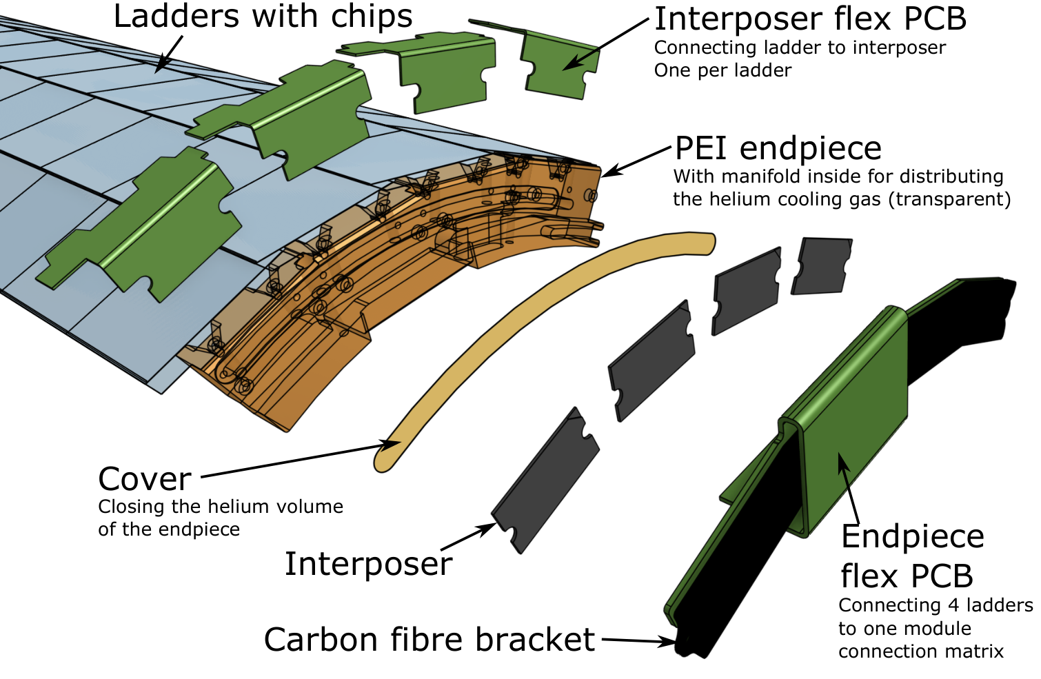
The endpieces of the outer layers have a fourfold segmentation and include an internal open volume to distribute helium gas for the cooling-system, see Figure 15. To realise the internal volume for helium distribution the endpieces are manufactured out of a main part with a thin lid, glued on, to seal the open volume after machining. The endpieces also accommodate the interposer connectors for power, control and data transmission.
7 MuPix Ladder Integration and Chip Bonding
During fabrication of the MuPix ladders, chips are placed accurately on the HDI by use of fiducial marks on the chips and cut-outs on the HDI. The chips are then glued using an epoxy (Araldite 2011), applied in small dots of thickness, and the positions are checked again. The flex circuit for connecting to the interposer is placed and glued in a similar manner. After curing, all connections between the HDI and each chip, and between the HDI and the interposer are SpTA-bonded (any vias on the HDI are bonded beforehand by the manufacturer). Once all the connections are in place, the unit is electrically fully functional. This allows for the comprehensive quality testing of a MuPix ladder before they are assembled into modules.
3 Pixel Tracker Global Mechanics
Pixel tracker inner and outer layer modules are integrated into the full cylindrical tracking layers by mounting the modules to the inner or outer layer pixel endrings. The latter in turn are connected to the up- and downstream beam pipes. Like the module endpieces these are manufactured out of PEI. For the inner layers the endrings have gas inlets and outlets to provide the helium flow between layers 1 and 2.

A drawing of an outer layer endring equipped with a layer 3 module is shown in Figure 16. The outer endring supports six modules of layer 3 and seven modules of layer 4. The endrings have dowel pins for every module to guide the module when it is rotated into position, ensuring no accidental collision happens with already mounted modules during installation. The final mechanical connection is done with screws. This also secures the contact through the endring interposer which provides the further electrical connection from the module, via the front-end flexprints, to the front-end boards, from where the steering and control of the MuPix sensors is handled and where the signal processing is done.
The outer layer endrings provide conduits for the helium gas flow between layers 3 and 4 and to the module endpieces for the gas flow in to the v-fold channels. At the upstream end, the inner and outer endrings are rigidly connected to the beam pipe. At the downstream end, the endrings are supported by bearings and connected via a small spring tension such that the downstream endrings can move along the beam direction to accommodate thermal expansion of the ladders.
4 Pixel Tracker construction and Quality Control
The production workflow of the pixel detector parts consists of manufacturing steps and quality control points, shown in Figure 17. The manufacturing steps make use of custom-made tooling for careful picking and accurate placing of parts.
To protect parts from damage and contamination, manufacturing will take place in controlled environments, e.g. cleanrooms of suitable levels, and standard ESD protection procedures will be in place. Polyimide expands when exposed to humidity. All manufacturing steps crucial to defining tolerances will be carried out in environments with strict temperature and humidity control and material will be stored therein for proper equilibration prior to use. At any other times during the production, storage or transport, components will be mounted in such a way to ensure thermal or humidity induced expansion can be accommodated safely. Raw parts are either obtained from suppliers (e.g. MuPix, HDI, interposer, etc.) or made in-house using custom tooling (e.g. polyimide folds) or CNC machines (e.g. endpieces).
Quality control takes place before and after every manufacturing step. Tests include (but are not limited to): visual inspection, dimension control, electrical testing, and gas leak testing. All components and their test results are tracked and documented in a production database. Raw parts will be acceptance tested upon receipt. In case of the MuPix chips, electrical testing will take place on the wafer, and on single die after dicing, using appropriate probe cards. Thanks to the modular design of the process, full electrical testing of all intermediate products is possible and foreseen. This includes the possibility to check sensor response using lasers or lab-grade radioactive sources. In addition to checks of the electrical functionality at all stages of production, MuPix ladders will undergo a long term burn-in test.
1 Inner Pixel Layers: Ladder and Module Production
The full inner pixel production and assembly takes place at Heidelberg. The small nature of this detector part (18 ladders with 6 chips per ladder) makes a manual procedure a cost-effective choice.
Chips are positioned relative to each other and to the interposer flexes on a custom jig. The interposer flexes define the position of a ladder on the endrings. The positioning is done by moving the chips with a sliding block and fixating each chip at the desired position by vacuum (Figure 18). While the position of the first chip is defined by a stop edge, following chips are placed using a micrometer screw and by monitoring the chip-to-chip gap with a microscope22 2 Dino-Lite AM4515T8-EDGE, resolution of .

Epoxy (Araldite 2011) is applied to the chips and the interposer flexes manually in small dots. The HDI is aligned to the chips and flexes by fiducial marks on both parts under the microscope. Weights ensure flatness and a uniform distribution of glue. A finished prototype ladder on the jig is shown in Figure 19. Prototype construction has demonstrated a placement precision of and an average glue thickness of .

After curing, connections between the chips and the HDI and between the interposer flexes and the HDI are made using SpTA-bonding. From this point on, the ladder is electrically fully functional. Each ladder undergoes a basic functionality test including powering, configuration and the readout of each MuPix chip.
Ladders that pass all QA checks are mounted into half-shells on custom assembly tools (Figure 20). These tools, for layer 1 and layer 2, accommodate the module endpieces and are designed such that each facet can be brought into the horizontal position for ladder placement. The ladders are glued consecutively to the polyimide flap of the previously positioned ladder. Again, weights ensure flatness and a uniform glue distribution. At the same time, the ladders are attached to the PEI endpieces by clamping them to a stack comprising the end of the ladder, the interposer and the endpiece flex held by a carbon fibre bracket.

2 Outer Pixel Layers: Ladder and Module Production
Ladder assembly for layers 3 and 4 of the MuPix tracker takes place at the Oxford Physics Microstructure Detector (OPMD) Laboratory. To make a ladder, 18 (17) chips are positioned on a vacuum jig using a 4-axis gantry positioning system, integrated with vision and electro-valve controls, and custom built tooling (see Figure 21). A positioning accuracy within 10 microns (see Figure 22) is achieved. After this the interposer flex circuit is added, located by the jig, glue is deposited by a commercial machine vision guided liquid dispensing robot and the HDI is glued to the chips using a counter-jig. Connections between the sensor chips and the HDI circuits are made using SpTA-bonding. The completed assembly is reinforced with two V shaped, folded polyimide support structures glued to each ladder. The liquid dispensing robot is used to accurately apply the required epoxy to achieve 5 micron thick glue layers to adhere sensor chips to the flexprints and polyimide V-folds to the ladders.


The polyimide V-folds are repeatably aligned and joined to the ladders using a custom jig with linear rails and micrometer adjusters. Semi-automated non-contact metrology of components and completed ladders is performed with an optical probe on a coordinate measuring machine.


After testing, MuPix ladders are shipped to Liverpool, for the assembly into modules. Upstream and downstream module endpieces are mounted to a custom jig that defines the overall length of a module. Ladders are positioned and glued onto the endpiece. Glue is applied manually to the surface of the endpiece and inside the v-shaped cut-out in the endpiece, as well as to the underside of the end of each ladder and the outside of the polyimide v-channels. Weights are used to ensure flatness and a uniform distribution of glue. After four ladders are assembled into a module, the v-channels on the inward facing side of the module are sealed with additional adhesive and electrical connections are made by fixing a stack of the ends of the four ladders, four interposers and the endpiece flex with a single carbon fibre bracket. Modules are checked for gas flow and leaks and for electrical conformity.
5 Prototyping and System Tests
A programme of manufacturing thermo-mechanical prototype modules for both the inner and outer layers of the MuPix tracker has been used to develop and commission the assembly tooling and processes. At the same time the built modules are intended to provide a testbed, called the thermo-mechanical mockup (TMM), to develop and demonstrate the helium cooling concept for the MuPix tracker. Modules for the TMM provide a close match to the final detector in terms of their mass and materials used and provide the means to dissipate heat loads, matching those in the real detector into the structure. Circuitry to monitor temperatures is also incorporated. Modules are built out two types of ladders: Silicon heater ladders and Tape heater ladders.
Silicon heater ladders.
These ladders closely match the material stack of the final detector. Silicon heater chips (Figure 23) have been manufactured at the Max-Planck Halbleiterlabor in Munich using sputtered aluminium on silicon without a passivation layer. A meander with allows heat to be generated in the chip in the range of 1 to with similar voltages as for MuPix chips. An additional meander with is used as a resistance temperature detector (RTD) to measure the temperature in situ. The chips are thinned to thickness. Ladders are fabricated using adapted versions of the HDI with the same stack as foreseen for the detector (Figure 24). Connections are made with SpTA-bonding. The manufacturing steps needed and tooling used are the same as for detector fabrication, providing the ideal test bed to develop, commission and qualify the tooling and processes for the final detector production.
Tape heater ladders.
These ladders are simpler objects, based around an aluminium-polyimide laminate (Figure 25) resistive heating circuit that has the same shape as the HDI plus interposer flex assembly in the final detector. Laser cutting and etching are used to manufacture the tape heater flexes in sizes corresponding to inner ladders () and outer ladders (). To create a more realistic mechanical model and material budget, thick stainless steel dummy chips can be attached if needed for specific test purposes. This more cost-effective option is used for simpler manufacturing tests and to instrument most of the full TMM.
The TMM is assembled by assembling the silicon heater and tape heater ladders into modules and barrels using the same mechanical components as are use in the final detector. With the heating capabilities and all the cooling facilities in place, realistic measurements of the cooling and mechanical stability will be possible. Tests stands for intermediate and final assemblies have been developed in preparation for the final testing of detector assemblies. All manufacturing steps are taking place at the locations foreseen for detector fabrication.
An example of ladders manufactured for the TMM is shown in Figure 26.


6 Pixel Tracker Cooling
The full pixel detector will dissipate about of heat33 3 Throughout this section, heat from chips and losses in conductors inside the HDI are taken into account, summing up to the heat density used in the scenarios. in a conservative scenario assuming . The latest chip versions have shown a heat dissipation below . This heat load is used for our most realistic scenario. Table 5 shows expected heat load in each layer of the tracker under these two scenarios. The cooling system must keep the maximum temperature, anywhere in the pixel detector, safely below , given by the glass-transition temperature of the adhesives used for construction.
| Detector Part | Area | ||
|---|---|---|---|
| [] | [] | [] | |
| layer 1 | |||
| layer 2 | |||
| layer 3 | |||
| layer 4 | |||
| Recurl Station () | |||
| total |


| No. | Description | # | Inlet | Outlet | |||
| 1 | Gap flow vertex detector | 1 | 2.0 | +40 | 10 | 2.0 | -40 |
| 2 | Gap flow b/w SciFi and L3 | 1 | 6.9 | +25 | 10 | 0 | 0 |
| 3 | Gap flow b/w SciTile and L3 | 2 | 5.7 | +28 | 10 | 0 | 0 |
| 4 | Gap flow b/w L3 and L4 | 3 | 7.6 | +25 | 10 | 0 | 0 |
| 5 | Flow in V-folds L3 | 3 | 1.3 | +90 | 20 | 1.3 | -90 |
| 6 | Flow in V-folds L4 | 3 | 1.5 | +80 | 20 | 1.5 | -80 |
| 7 | Global flow, | 1 | 4 | +0.04 | var. | 45 | -0.04 |
| Total | 14 | 56 | 56 | ||||
We use gaseous helium at ambient conditions44 4 This means temperatures above and the absolute pressure around . as coolant. The helium is distributed in separate circuits, serving different parts of the detector separately. The concept is shown in Figure 27 and the different helium circuits are listed in Table 6. The flow in the global circuit increases along because of other circuits directly venting into the global flow. The global flow is constrained by a thin mylar foil (thickness ) surrounding the full pixel detector in a conical shape that keeps the helium velocity near constant along z (see Figure 6.
The system described is the result of a process of optimisations through simulation studies using computational fluid dynamics (CFD)55 5 Autodesk® and ANSYS CFX® CFD software were used. and verifications in the laboratory [29, 30, 31, 32, 33, 34]. The models used in both simulation and laboratory measurements progressed in detail and the final mock-up models described in section 5 match the final detector to a great extent in shape, materials and heat-density.
The heat-load density distribution used in the simulations take care of the uneven heat density on the pixel chip. Half of the power dissipation on the chip is expected to be located on the periphery, the remaining half within the pixel matrix, equivalent to and respectively, for an averaged in the conservative scenario. Simulation results for the pixel tracker are shown in Figure 28, confirming a safe even in the conservative scenario. In simulations with the realistic scenario the obtained values have been found to scale down linearly with the reduced power dissipation and are therefore not shown.
The experimental cooling tests were performed inside a cylindrical closed volume with a diameter of and a length of approximately . Helium was initially provided by compressed gas bottles, limiting measurements to a few minutes. This was overcome by using a miniature turbo compressor (described in chapter 11) allowing for helium recirculation and hence continuous operation. The agreement between simulation and mock-up measurements are good, see Figure 29 for an example comparison for the vertex detector [35].


Vibrations induced by the helium flows must not damage the structures or have a substantial impact on the hit resolution. Such vibrations were studied using a setup based on a Michelson interferometer pointing to reflective surfaces on a realistic mock-up. For velocities up to , average amplitudes of were observed, with peaks of [36, 32, 37]. This is well below the single hit resolution of the pixel sensors. An excitation spectrum using a speaker showed resonances between to with no major peaks. No damage to the test structures has been observed during these studies.
Chapter 7 MuPix Pixel Sensor
The very challenging requirements on the allowed amount of material in the tracking layers can only be fulfilled with a monolithic silicon pixel technology. Monolithic sensors efficiently integrate sensor and readout in the same device, thereby greatly reducing the detector material in comparison to classical hybrid pixel module designs, which require additional readout chips and interconnects (bonds). For the Mu3e pixel detector, High-Voltage Monolithic Active Pixel Sensors (HV-MAPS) [23] were chosen. They are produced in a commercial HV-CMOS process [38] and can be thinned to to reduce material [39].
For Mu3e an experiment-specific HV-MAPS, the MuPix, has been developed. All MuPix sensors in the pixel tracker are the same size, each instrumenting an (active) area of about . The main parts of the digital electronics are located in the chip periphery, a region about wide on one side of the sensor. The periphery also integrates dedicated pads for SpTA-bonding [24] (see chapter 6), and additional pads for testing. The number of electrical lines to operate the sensor is kept to a minimum in order to reduce the number of interconnects and to ease routing. All electrical connections for signal, control and monitoring are differential and run at high speed. Additional connections are provided for power, ground, bias-voltage, and for passive temperature monitoring using a diode.
All MuPix sensors will be operated synchronous to the Mu3e system clock with precision. This alignment is achieved by means of a synchronous reset command. Hit timestamps are derived from an internal phase-locked loop (PLL) running at a nominal frequency of . Data are sent over up to three configurable serial links, each providing a bandwidth of using an 8 bit/10 bit encoding protocol.
Operating temperature, and therefore the power consumption of the MuPix sensors, is critical for the tracking detector. We have tested and qualified HV-MAPS for temperatures up to but define a maximum temperature of to stay in the specified range for the adhesives used in the tracking detector. The minimum temperature is defined by the icing limit (section 6). The power consumption of the pixel tracker per unit area must not exceed the maximum cooling capacity of the helium gas cooling system, , see chapter 11. Taking into account electrical losses on the HDI and power cables, the MuPix sensor must therefore be operated below the power consumption limit of . The main requirements for the pixel sensor are summarised in Table 1.
| sensor dimensions [] | |
| sensor size (active) [] | |
| thickness [] | |
| spatial resolution | |
| time resolution [] | |
| hit efficiency [] | |
| #LVDS links (inner layers) | 1 (3) |
| bandwidth per link [] | |
| power density of sensors [] | |
| operation temperature range [] | 0 to 70 |
After introducing the HV-MAPS concept, an overview of the MuPix R&D and the characterised prototypes is given. The final MuPix design is presented in section 3. The main results obtained by prototypes are discussed in section 4 including first characterisation results from the final MuPix10 prototype.
1 HV-MAPS
HV-MAPS collect ionisation charge mainly via drift and therefore provide time resolutions of a few nanoseconds, in contrast to standard MAPS [40, 41, 42, 43, 44, 45] which collect ionisation charge mainly by diffusion with a typical timescale of several hundreds of nanoseconds. In standard MAPS, the in-cell electronics is implemented outside the n-well which serves as charge collecting diode (sometimes referred to as “small fill factor” design). In HV-MAPS, instead, the pixel amplifier electronics is implemented inside the deep n-well, see Figure 1. By reverse biasing the charge collecting diode with high voltage () the substrate of the pixel cell is depleted. Using the HV-CMOS process developed by IBM (or variants), this HV-MAPS concept was first proposed in [23] and has been successfully tested with several prototypes since [46, 47, 48, 39, 49, 50]. In recent years, the concept of depleting MAPS was successfully applied also on other technologies, see e.g. [51, 52].
At maximum high-voltage, the size of the depletion zone is below for low-ohmic wafer substrates , as confirmed by edge-TCT characterisation [53]. As the stack containing the electronics and metal layers is only for the technology used, it is possible to remove substantial parts of the substrate that do not contribute to the charge generation process. Therefore, HV-MAPS can be produced with a thickness of , corresponding to about . Depending on the choice of the substrate, up to about primary electrons are expected for minimum ionising particles with trajectories perpendicular to the plane of the substrate.
Specific for all MuPix designs is the spatial separation of charge-sensitive amplifiers (in the active pixel matrix) from the comparators (in the chip periphery with the readout circuitry). Each pixel cell implements a source follower which drives the analogue signal to the periphery, see Figure 2.
The MuPix readout circuitry provides zero suppression and generates timestamps to enable time-matching of hits from different pixel layers. For MuPix8 and later generations, a second timestamp is generated to provide time-over-threshold (ToT) information. Offline, the ToT information can be used for time-walk corrections, better noise suppression, and for improving the spatial resolution by means of charge sharing.
After hit detection and digitisation, an internal state machine collects all hits using an address prioritisation scheme. Data are sent via up to three serial links at a nominal data rate of each using a simple protocol with time frames and 8 bit/10 bit encoding. Alternatively, in the multiplexed mode it is possible to use only one serial link.
1 HV-CMOS Process and Manufacturers
The H18 HV-CMOS process was selected based on the high level of achievable integration, and the positive results from prototypes for high rate capability, timing resolution and efficiency. The breakdown voltage of the IBM HV-CMOS process is or greater, depending on the design rules. The maximum available reticle size depends on the manufacturer, and is slightly larger than the envisaged chip size of about for all foundries.
The HV-CMOS process was originally developed for the automotive industry and thus offers long-term availability as well as specifications covering a wide range of operating conditions. Although the HV-CMOS production costs are higher than for standard CMOS processes, they are significantly lower than for hybrid silicon sensors, thus making the large Mu3e pixel detector with an instrumented area of about affordable.
The original HV-CMOS process from IBM [54] was offered by ams AG 11 1 ams AG, Austria, http://www.ams.com until 2015 and was used for the production of several prototypes including MuPix7. In 2017, ams AG changed to a new in-house developed process which was announced to be similar to the original H18 process from IBM and used for the production of the MuPix8 and MuPix9 prototypes.
The HV-CMOS process from IBM is also offered by GlobalFoundries Inc.22 2 GlobalFoundries Inc., USA, https://www.globalfoundries.com and TSI Semiconductors 33 3 TSI Semiconductors, USA, http://www.tsisemi.com. In contrast to GlobalFoundries, TSI also offers chip production with non standard substrates. This allows for higher resistivity substrates and thus higher charge collection signals. In addition, TSI provides seven metal layers instead of six (ams AG). This feature is crucial for the reduction of cross-talk (see the next section). Also for cost reasons, we have chosen the HV-CMOS process from TSI as baseline for the production of the MuPix sensor. Since 2018, several HV-MAPS have been successfully produced at TSI.
2 Limitations and Design Challenges
The high bias voltage of the HV-MAPS concept requires a careful design of the pixel cell geometry. TCAD simulation [55, 56] is mandatory for the design to avoid large field gradients which lead to early breakdown. The large fill factor of the HV-MAPS cell design implies relatively large pixel capacitances, thus increasing noise, compared to the more standard “low fill factor designs”. As a general design principle, pixel capacitances should be minimal since they lead to signal deformation and increase time-walk effects, thus compromising the maximum achievable time resolution. Large pixel capacitances can be partially compensated by amplification stages with larger gain. However, this goes along with a high power consumption and also increases the risk of electronic cross-talk.
A limitation of the MuPix concept is related to the long analogue readout lines from the pixel cell to the periphery, see Figure 2. These long interconnects (up to ) have large capacitive couplings with the neighbouring lines and are prone to cross-talk, strongly dependant on the spacing of the readout lines – and thus on the number of available metal layers for routing. To reduce cross-talk, several mitigation strategies have been studied. With MuPix prototypes, special multi-layer routing schemes which reduce the coupling between readout lines were implemented and tested. In addition, dedicated routing topologies – one of the simplest being split readout of even and odd rows, see Figure 3 – can be used to differentiate between charge sharing among neighbouring pixels and cross-talk between adjacent signal lines. Furthermore an approach with a two-stage amplifier was studied [57] but not further considered. Detailed cross-talk measurements have been performed with the MuPix8 prototype and are discussed in more detail in section 4.
2 MuPix Prototypes
Nine prototypes were produced so far in preparation of the Mu3e experiment, the latest being MuPix10. The layout of selected prototypes is shown in Figure 4. Their specification and measured performance parameters are listed in Table 2, compared with the main Mu3e requirements.

| Requirements | MuPix7 | MuPix8 | MuPix10 | |
| pixel size [] | ||||
| sensor size [] | ||||
| active area [] | ||||
| active area [] | ||||
| sensor thinned to thickness [] | , , | , | , | |
| LVDS links | ||||
| maximum bandwidth§ [] | ||||
| timestamp clock [] | ||||
| RMS of spatial resolution [] | ||||
| power consumption [] | ||||
| time resolution per pixel [] | not meas.‡ | |||
| efficiency at noise [] | ||||
| noise rate at efficiency [] | ||||
| amplifier type | no spec. | PMOS | PMOS | PMOS |
| amplifier stages | no spec. | 2 | 1 | 1 |
| timestamp representation | no spec. | 8 bit | 10 bit | 11 bit |
| ToT representation | no spec. | - | 6 bit | 5 bit |
| ring transistors (irradiation tolerant) | no spec. | no | yes | yes |
| approx. substrate resistivity¶ [] | no spec. |
The MuPix7 sensor [58] was the first prototype which included all main functionalities required for the Mu3e experiment: a fully integrated readout state machine, high speed clock generation circuits (PLL) and a fast serial output link running at up to , able to drive signals over . The MuPix7 sensor has an active area of about .
The MuPix8 sensor [49, 59] was the first large scale sensor produced in an engineering run and was produced with different p-substrate resistivity. Unlike previous prototypes, MuPix8 was produced in the new AH18 process by ams AG. MuPix8 features a more radiation tolerant design44 4 The HV-CMOS process has been qualified for fluences of up to (1 MeV) neq in the context of the ATLAS high luminosity upgrade [60, 61, 62, 59]. and is prepared for high data rates by implementing three additional serial links. Furthermore, a second time stamp was added to measure ToT, thereby enabling the offline correction of time-walk effects due to pulse height variations. The main purpose of the MuPix8 prototype was the study of topics related to the size of the sensor: the power network design and potential cross-talk between the long analogue readout lines.
Special system aspects relevant for the construction of the pixel tracker were addressed with the dedicated small area MuPix9 sensor which features fast differential control inputs, a new chip configuration scheme and a shunt-Low Drop Out (LDO) regulator to study serial powering.
MuPix10 is the final prototype, prepared for the construction of pixel modules. The active area is . The pad layout is compatible with the spatial requirements of the pixel modules and the HDI design rules. The sensor was produced at TSI in an engineering run and delivered in March 2020.
In the following, the final design of the MuPix sensor – as it will be used in the Mu3e experiment – is described.


3 MuPix Final Design
The pixel cell has a size of , and the pixel matrix is divided into three sub-matrices (A-C), consisting of 42+43+43 double-columns. In total there are 256 pixel columns and 250 pixel rows. Readout of hits in the three sub-matrices are handled by state machines. Depending on the readout mode, hits in the three sub-matrices are sent to corresponding serial links SOUT1-SOUT3 (high bandwidth mode) or to a common readout link SOUTX (multiplexed mode). Hits read from a pixel column are collected at the end of the column using address prioritisation. This implies that the hits are not in chronological order.
A block diagram of the MuPix10 layout is shown in Figure 5 and the main function blocks are detailed in the following.
1 Pixel Cell Electronics
The layout of the pixel cell housing the amplification circuitry is shown in Figure 6 for MuPix10. Each pixel consists of the sensor diode, a charge-sensitive amplifier and a source follower to drive the signal to the chip periphery, see Figure 7. Every pixel has a capacitor allowing to inject test charges. As baseline the implementation of a PMOS-based amplifier with source follower is chosen. Pulse shaping is adjustable via bias currents with typical shaping times of . The size of the charge collecting diode was optimised using TCAD simulation, to ensure a homogeneous electrical field, for a substrate resistivity of and a depletion voltage of . The guard ring was optimised with a design goal of for the breakdown voltage.
2 Readout Buffer Cell
For all MuPix designs the digital electronics was placed at the chip periphery. This design decision was motivated by the goal to reduce cross-talk between the quickly switching digital signals and the sensitive analogue circuits. The Readout Buffer Cell occupies about , corresponding to about 10% of the active cell, and covers two pixel columns in width (double column routing). The main functionalities of the Readout Buffer Cell are described in the following.
Comparators convert the analogue signal into an arrival time signal. The common threshold for the comparators is set globally. Individual 3-bit digital-to-analogue converters (DAC) allow for fine-tuning the threshold for each pixel. This feature can be used to ensure an uniform signal response or noise suppression over the pixel matrix. A fourth enable bit can be used to mask out noisy pixels. For test purposes, the comparator output of pixels can be monitored via a dedicated output line (hitbus signal).
A hit is defined by the rising edge of the comparator output. For timestamp generation the output is sampled with an adjustable frequency derived from the internal clock.
For the latest MuPix prototypes, a second comparator was added to each Readout Buffer Cell. The 2-comparator threshold scheme allows the implementation of a very low threshold (close to noise) for measuring the time-of-arrival (ToA) of the rising edge with little time-walk, and a high threshold (well above noise) for the generation of the hit flag, see also Figure 8. This scheme proved successful with the MuPix8 prototype, for which an improvement of the time resolution was demonstrated [63]. In MuPix10 it is possible to use only one comparator or a mixed mode where the ToA is defined by the lower threshold and the time-of-fall by the higher threshold. The mixed mode features time-walk mitigation and, additionally, provides robust ToT information for a residual time-walk correction.
In MuPix10, the timestamp is represented by 11 bits, and the ToT by 5 bits. Both measurements are sampled with adjustable frequencies derived from the internal clock. All counters are implemented as Gray counters and ToA and ToT are stored in floating capacitors55 5 Actually, the time of the falling edge is stored from which the ToT is calculated at a later stage. MuPix10 can be operated in different modes; with only one comparator or with two comparators where the ToT measurement can be taken either from the lower or higher threshold (configurable).
In MuPix10, the hit-flag is generated by a hit-delay circuit with a programmable timer in order to avoid huge sampling times for signals with large ToT values. The purpose of the hit-delay circuit is two-fold: first, it makes the hit-flag generation independent from the pulse-height and helps to keep the chronological order of the hits; second, it reduces dead-time by cutting out long sampling times. The impact on ToT-based time-walk corrections is minor since time-walk effects are small for large signals.
3 Pixel Routing
The routing for MuPix10 is slightly more complex due to the double column RO scheme, i.e. two pixel columns are read out by one column of hit buffers. In addition, a special routing scheme has been implemented by fully exploiting two metal layers with the goals to A) reduce signal line cross-talk, B) enabling the identification of signal line cross-talk and C) reduce row dependent time delays. In comparison to a conventional comb-like routing scheme, cross-talk is reduced by implementing a scheme where neighbouring lines are at their closest proximity at only for of the total column length. This routing scheme is fully described in [64, 65]. The expected cross-talk rate is discussed in subsection 2.
The identification of remaining cross-talk is achieved by the addressing choice: neighbouring signal lines are not connected to neighbouring pixels, see Figure 3. Physical space and address space are consequently defined differently. Cross-talk is expected to show (triplet) clusters in the address space whereas charge sharing among pixels cells creates clusters in physical space.
Furthermore, row dependent time delays are caused by signal line differences in the capacitive coupling and ohmic losses. In MuPix10 only four different lengths of the signal lines are routed. Therefore, the time distribution of hits is expected to show 4 discrete delays only.
4 State machine
Finally, the internal state machine reads out the all the hit information (address, timestamps and ToT-values) from the Readout Buffer Cells. We now describe the readout logic as implemented in the chip internal state machine.
The readout scheme follows a standard column drain architecture, see Figure 9. A readout cycle starts with the issuing of the LdPix signal. The hit flags, generated by the hit delay circuit, are then stored in a second register/latch. Hits arriving after LdPix will only be considered in the next readout cycle, thus preventing race conditions due to hot pixels. In the next step, the column buses are cleared. Then, the LdCol signal is sent to all columns. By exploiting priority logic the RdPix signal is generated for the highest priority pixel containing a hit. RdPix reads the corresponding buffer cell and drives timestamp information and the row address on the column bus. These signals are registered at the end of column (EOC). The corresponding pixel is reset (initiated by RdPix) and is ready to accept the next hit.
If at least one column (or rather EOC) contains a hit, the RdCol signal is issued, upon which the column with the highest priority drives the EOC data (containing timestamp information and row address) and the column address to the serialiser, and then resets itself. This is repeated, until all columns are empty. Then the next hit in each column is loaded to the column periphery, and so on. The speed of the state machine is adjustable.
5 Clocking and PLL
The MuPix is synchronised to an external clock and generates internal clocks for hit sampling, the state machine and the serialiser. It contains a tunable voltage controlled oscillator (VCO), running at up to , and a PLL to keep the VCO in phase with respect to the reference clock. The various stages of the serialiser, the readout state machine, and the timestamp counter all run at frequencies which are adjustable integer divisions of the fast base clock. MuPix prototypes have been operated at a sampling frequency of (MuPix7) and (MuPix8); a sampling frequency of up to was also successfully tested.
6 Serial Links and Data Output
After serialisation the data are sent out via fast serial links, which are clocked with the internal fast clock () which corresponds to 5 times the reference clock frequency (). Data are sent at both, the rising and falling edge of the clock, corresponding to a bandwidth of per link. Pre-emphasis of the signal can be controlled via bias currents to reduce rise and fall times. Each LVDS links consumes about of power.
Data are packed in 32 bit words which include the hit address (8 bit for column and row address each) and Gray-encoded timestamp information (11 bits for time-of-arrival and 5 bits for ToT). Data on the serial link are 8bit/10bit encoded, using the standard IBM encoding [66, 67]. Operating at , this leaves up to for user data. Comma words are used to define event frames and ease synchronisation of the data. The data protocol [64] also foresees the sending of slow control data.
In the high bandwidth mode three serial links are operated in parallel, yielding a nominal data rate of with a total payload of . In the multiplexed mode the state machine is alternately reading hits from the three sub-matrices which are sent to a common serial link. The configuration of the RO-mode is done by control commands.
7 Powering and Configuration
The final MuPix will work with only one supply voltage of (at chip) from which the internal VSSA is generated using an LDO which can also be bypassed by extra pads. A power up reset, with a duration not exceeding , is implemented to ensure that the chip starts up in a stable configuration with only minimal power consumption (standby mode). Only the slow-control block is directly connected to the supply voltage line, all other bias blocks are by default disabled after power reset and need to be switched on by control commands. The standby mode should allow for basic communication with the chip without dedicated cooling measures.
All capacitors required for power reset, power regulators and noise decoupling are implemented in-chip. The chip is designed such that no external de-coupling capacitors and pull-ups or pull-downs are needed.
Control and configuration of the chip is possible over a differential serial link (SIN). 64 bit long commands are used to fill the shift registers. The decoding of the commands is handled by a slow control state machine. The shift registers Bias, Config and VDAC are responsible for the global chip configuration. The shift registers Col, TDAC and Test are responsible for the configuration of the test infrastructure (injection, ampout, hitbus), as well as the pixel tuning.
8 Monitoring
Monitoring information is primarily sent via the LVDS links. An ADC is implemented to measure several internal voltages, such as thresholds, baselines and regulated power, as well as temperatures using thermo-circuits [64]. The ADC readout can be configured via special control commands - for example, it is possible to read out all slow control parameters round robin. The ADC measured voltages can also be tapped by additional slow-control outputs. The ADC is in the same power block as the slow-control and always operational.
| Pad | # pads | IN/OUT | type | routed | description |
|---|---|---|---|---|---|
| GNDD | IN | mand. | GND | digital ground | |
| GNDA | IN | mand. | GND | analog ground | |
| VDDD | IN | mand. | VDD | power supply | |
| VDDA | IN | mand. | VDD | power supply | |
| VOUTS | OUT | select | - | regulated voltage out | |
| VSSA | IN | mand. | - | regulated voltage in | |
| BIAS | IN | mand. | BIAS | HV bias voltage (bus) | |
| CLK | IN | diff. | CLK | system clock | |
| SIN | IN | diff. | SIN | control bus | |
| SOUTX | OUT | diff. | SOUTX | multiplexed LVDS data output | |
| SOUT1 | OUT | diff. | SOUT1 | LVDS data sub-matrix 1 | |
| SOUT2 | OUT | diff. | SOUT2 | LVDS data sub-matrix 2 | |
| SOUT3 | OUT | diff. | SOUT3 | LVDS data sub-matrix 3 |
An additional analogue temperature measurement is implemented to allow measurements if the chip is not powered or configured. This circuit is optimised to be maximally sensitive the temperature range of with . This diode is externally connected to power and floating if the chip is not powered.
9 I/O and Pad Layout
For the construction of MuPix modules the number of inputs and outputs required to operate the chip must be kept at a minimum. In total only 9 (13) lines have to be connected to operate the sensor in the multiplexed (high bandwidth) RO mode, assuming that common ground (GNDD=GNDA) and power (VDDD=VDDA) are used for the digital and analogue domains. The list of mandatory connections is shown in Table 3. Multiple pads are implemented for power and ground to reduce ohmic losses. The usage of a power regulator to generate VSSA internally is hardware configurable66 6 Actually, two parallel regulators are implemented for distributing the power dissipation over a larger area at the periphery.. All differential lines are ESD protected. For all mandatory connections two different types of pads are implemented: standard wedge bonds for chip tests and SpTA-bonds for pixel module production. Additional standard pads are implemented for chip characterisation studies. They enable monitoring of internal signals, thresholds and voltages. The pad size for wedge bonds is . The pads for SpTA-bonds have a size of and fulfil the specification for bonding the aluminium-polyimide HDIs produced by LTU.
4 Performance of MuPix Prototypes
As of 2020 nine MuPix prototypes have been studied by exploiting different techniques for chip/sensor characterisation: injection pulses, LEDs, laser diodes, X-rays, radioactive sources and test beam campaigns. The main results obtained from the latest MuPix prototypes are presented here. Emphasis is given to results obtained from MuPix8 which was thoroughly studied and has a design very similar to the final MuPix.
1 Single Hit Efficiencies
Single hit efficiencies of MuPix sensors were determined in test beam campaigns at CERN (Geneva), DESY (Hamburg), MAMI (Mainz) and PSI (Villigen). Studies were performed as a function of various DAC and HV settings for different comparator thresholds and powering schemes. Beam telescopes were used for the reconstruction of reference tracks and the measurement of single hit efficiencies. The efficiency map and noise map for a MuPix8 sensor produced with an substrate is shown in Figure 10.

In Figure 11 the single hit efficiency of the same MuPix8 sensor is shown as a function of the threshold. This sensor was operated at a bias voltage of and noisy pixels have not been masked. The Mu3e efficiency and noise requirements are fulfilled in a large threshold range of about -, corresponding to about -. This high efficiency range can be further extended by tuning the individual pixel thresholds, by masking noisy pixel and by increasing the bias voltage. This measurement confirmed the expected increase of the depletion area, and the resulting hit efficiency, by using a higher resistivity substrate than the standard . The increase of the depletion region is also supported by TCAD simulations [69] and HV-CMOS characterisation studies including Edge-TCT measurements [53]. For substrate resistivities of an even wider plateau of high efficiency has been obtained [70].
2 Noise and Cross-Talk
For optimised DAC settings a noise of about 90 electrons was measured for MuPix8 using a threshold scan. The source is mainly thermal noise from the capacitances of the diode and the amplifier input transistors. The noise figure has to be compared to the expected number of primary electrons which strongly depends on the substrate resistivity. For the envisaged substrate of and approx. depletion more than primary electrons are expected in the experiment.
Another source of noise is cross-talk which is particularly dangerous in mixed signal designs where frequently switching signals in the digital circuitry induce noise in the analogue section. Various tests have been performed and no cross-talk from the digital section was detected for reasonable hit thresholds, even when the MuPix prototypes were operated at very high readout rates (), thus confirming the MuPix design.
Cross-talk between pixel cells was studied by analysing hit correlations. Hit correlations are naturally expected from charge sharing if tracks create ionisation charges in the vicinity of two pixels inside a cone of about [68]. A clear correlation between the position of the charge deposition and charge sharing was seen in test-beam measurements but no significant cross-talk between pixels could be measured.
Significant cross-talk, however, was observed in MuPix8 between the long analogue readout lines connecting the pixel cells with the comparators in the periphery, see Figure 2. Figure 12 shows the signal measured at the comparator inputs of adjacent pixels in the same column after injecting a pulse to the middle pixel. In MuPix8 a conventional comb-like routing scheme was implemented where the length of RO lines scales linearly with the row number. This scheme allows a detailed study of the cross-talk probability as a function of the row number, and thus the length of the RO line. The capacitive coupling has been derived from the amplitude ratios of injected to measured signal, and was found to be proportional to the length of the readout line, see Figure 12, with a signal loss of roughly 0.155 % per pixel row. Small deviations from linear behaviour are expected and due to non-linear routing effects, e.g. change of metal layers.
The capacitive coupling between RO lines leads to a specific triplet pattern, see discussion of Figure 3. The frequency of this cross-talk has been derived from test-beam data as a function of the row number and is shown in Figure 13. The triplet pattern probability above row number shows a linear increase with the length of the readout line. For the highest row numbers, corresponding to a signal line length of , the probability is approx. 35% that a triplet pattern fires.
From the MuPix8 characterisation results the capacitive coupling between RO lines is estimated for MuPix10 to be %, considering the improved routing scheme (see subsection 3) and the 20% increase of the signal line density. For most hits, the amplitude of the cross talk signal is expected to be small enough to be below detection threshold. If the cross-talk is above the hit threshold, special easy-to-identify patterns will emerge due to the MuPix10 routing scheme.
3 Time Resolution
Several effects contribute to the timing of hits in a monolithic sensor: pixel-to-pixel variations in the amplifier response, signal routings of different length, effects due to variations of the signal amplitude (time-walk), discretisation due to the timestamp sampling and jitter due to noise. The time resolution was studied in detail for the MuPix7 and 8 designs.
For MuPix7, which has a special diode structure in the pixel cell, small time variations depending on the spatial position within the cell have been measured [58] with the high resolution EUDET telescope at DESY. These variations can be explained by inhomogeneities in the charge collecting field and were found to be about , much smaller than the measured time resolutions of MuPix7 of about which is dominated by time-walk effects.

Hit delays over the matrix were studied in detail with the first large scale sensor, MuPix8. Hit delay variations were found to be significant, see Figure 14. A strong position dependence is measured which is more pronounced as a function of the row number. The time difference between the lower left edge and the upper right edge is more than as measured with a 90Sr source. For the hit delay and its spatial variation a strong dependence on the DAC settings and the supply voltages was observed. For MuPix10 the hit delay variation could be reduced with the new routing scheme of the readout lines where all traces in one out of four blocks have identical lengths [65]. In addition the power net was improved such that the total delay variation is reduced by about a factor . Time variations over the sensor can be corrected either offline or in the Mu3e filter farm. Therefore, they are not relevant for the ultimate time resolution achievable with the pixel detector system.
Next, the impact of time-walk on the time resolution is discussed. Figure 15 shows the measured correlation between ToT and time-walk for MuPix8, which was determined with respect to a scintillator reference using a beam of electrons. Here, the timewalk is plotted for all pixels after applying a delay correction dependent on pixel position (see above). A mean shift of the time-walk of about is seen between large signals (large ToT) and small signals (small ToT) which can be corrected for on average by using the measured ToT information.
After correcting hit delays, overall a time resolution of is obtained. The ToT information can be used to further improve the time resolution and the results are shown in Table 4. Time resolutions before and after time-walk correction are given here for row numbers , where signal losses due to the capacitive coupling between RO lines are small. The numbers are given for the standard method and the 2-comparator threshold method where the first threshold is below the second threshold. For both methods a significant improvement of the time resolution is achieved by applying time-walk corrections. In contrast, the improvement of the time resolution by using two thresholds is small, both with and without the time-walk correction.
| time-walk correction | ||
|---|---|---|
| w/o | with | |
| (1 comparator) | ||
| (2 comparators) | ||
The time resolutions listed in Table 4 are still affected by pixel-to-pixel variations of the hit delay parameters. These variations can be accounted for by measuring the time resolutions for individual pixels. The resulting time resolution using the 2-comparator threshold method and after applying a time-walk correction is shown for all pixels in Figure 16. An average time resolution of about is obtained. The spread of time resolutions is small but there is a trend that the best time resolutions are obtained for pixels with a small row number. Taking into account the sampling frequency of , the intrinsic time resolution is estimated to be on average.
To conclude, the MuPix8 sensor with a substrate resistivity of fulfils the time resolution requirement of even without applying corrections. The excellent time resolution is beneficial for the Mu3e experiment and can be used to reduce combinatorics in the online reconstruction of tracks (in the filter farm) and offline.
4 Temperature Dependence
The temperature dependence of the MuPix design has been investigated for prototypes in the temperature range of to using a climate chamber. The actual sensor temperature was not monitored in these measurements but known from infrared measurements to be typically - higher. The temperature dependence was studied for both the analogue and the digital part. As expected the hit noise was found to increase by about a factor in the temperature range from [72]. At the same time the amplified signal was found to significantly decrease, see Figure 17. The MuPix prototypes were fully operational in the targeted operation range. The PLL was successfully locking at all temperatures and no significant increase of clock jitter was measured, even at the highest temperatures. However, in order to keep the signal-to-noise ratio high, the MuPix temperature should not exceed .
5 Power Consumption

The power consumption of MuPix sensors, and thus their heat dissipation, depends strongly on the amplifier and other DAC settings. Studies of prototypes have shown that high performance operation points can be found if the power consumption normalised to the active area is (see Table 2). But MuPix prototypes can also be operated at significantly higher power consumption, for example when aiming for better time resolutions. For the final MuPix sensor the total power consumption will depend on the readout mode and the powering scheme. If three LVDS links are used (high bandwidth mode for inner vertex layers) the total power consumption is about higher compared to the standard operation with one multiplexed link77 7 Dis-/Enabling of the LVDS links has not been implemented in existing prototypes but will be implemented in the final MuPix sensor.. Furthermore, the VSSA voltage can be externally provided or generated in-chip with a regulator. The latter is the standard operation for Mu3e and adds another , corresponding to a relative power increase of 10%. First characterisation measurements of MuPix10 are consistent with previous results obtained from MuPix7 and MuPix8, and suggest that the final sensor can be safely operated with all LVDS links running with a power consumption of , well below the critical cooling limit of .
6 LVDS Links
The quality of the serial data links has been extensively studied for the MuPix7 and MuPix8 prototypes using bit error rate measurements and eye diagrams. For tests the signal was transferred over SCSI-2 twisted pair cables up to long, from the sensor to an Altera Stratix IV FPGA development board. In this long test, no errors were found, giving an upper limit on the bit error rate at 90% confidence level.
Figure 18shows the eye diagrams of the four LVDS links of MuPix8 at without pre-emphasis. A degradation of the eye opening from link 0 (width = , height = ) to link 3 (width = , height = ) is visible. Moreover, the jitter of link 2 was found more than 25% larger than that of the other links. This degradation of the signal quality from link 0 to link 3 is probably caused by an in-chip drop of the voltage in MuPix8.
7 Irradiation Effects and High Rate Tests
High particle rates increase the readout dead-time and can also lead to irradiation damage. For Mu3e, bulk damage of the MuPix sensor due to non-ionising radiation (fluence (1 MeV) neq for Phase I) is considered to be negligible. The situation might be different for ionising radiation which can lead to oxide damage in transistors. In Mu3e, the ionising dose is expected to be highest in the inner-most vertex layer; not only from Michel decays electrons but also from scattered muons that miss the target and stop on the innermost vertex layer where they deposit all their kinetic energy.
The impact of large irradiation doses to the MuPix sensor was studied in test beam campaigns at MAMI and PSI. For several prototypes, temporary damage was measured in the electron beam at MAMI if the beam intensity exceeded and if the sensors were operated in the avalanche region which starts at about . The temporary damage caused a loss of the signal detection efficiency and lead to an “after-glowing” (noise) of the irradiated region with a time constant of minutes to hours. Similar effects were also observed at PSI in a pion beam-line. These effects were only seen at rates which exceed the Mu3e Phase I conditions by several orders of magnitude. A dedicated campaign where MuPix sensors are irradiated with a strong 90Sr source for long periods is ongoing.
The impact of high particle rates on the hit detection efficiency due to dead-time in the pixel readout cell is shown in Figure 19. The efficiency was measured using an extremely focused electron beam at MAMI with local beam intensities of up to . A degradation of only 3 permil was measured at rates which exceed the expected rates in Mu3e. The degradation is caused by dead-time in the pixel readout cell.
8 Mupix10 results

The MuPix10 prototype was delivered by TSI in May 2020, manufactured on substrate. This prototype could be successfully brought to operation and is currently being characterised in the lab and in test beam campaigns at DESY and PSI. At time of publication the characterisation studies of MuPix 10 have just started and preliminary results are presented in the following. Figure 20 shows the MuPix10 hit map as measured at DESY in a beam with electrons without any tuning of the sensor. All pixels are operational and no noisy (hot) pixels are visible. First results indicate that the efficiency and noise performance of MuPix10 is similar to MuPix8.
A new feature of the MuPix10 prototype is the adjustable timer delay readout. Figure 21 shows the ToT distribution of pions as measured for different timer delays. The peak at the end of each ToT distribution is due to the readout timer delay which slightly varies for different pixels and hits. This new feature limits the readout time (and therefore dead-time) without affecting the measurement of small or medium signal amplitudes where time-walk corrections are important.

Finally, Figure 22 shows the threshold distribution of injected charges for a block of pixels before and after calibration. The spread of the pixel thresholds can be significantly reduced from (corresponding to electrons) to (corresponding to electrons). These numbers can be compared with the expected signal amplitude of about signal for a MIP ( electrons) and a measured noise of about (corresponding to electrons) after TDAC tuning.
Further measurements of the MuPix10 sensor indicate a similar or even better performance than the one obtained for MuPix8. All preliminary results obtained so far suggest production readiness. The final sensor, the MuPix11, will include only minor improvements, most importantly a fix in one of the configuration lines. It will be produced in 2021 for constructing the Mu3e pixel tracker.
Chapter 8 MuTRiG
A common Application Specific Integrated Circuit (ASIC) has been developed for both the fibre and tile detectors in Mu3e, capable of operating with the rather different conditions of the two systems.
1 Introduction
MuTRiG (Muon Timing Resolver including Gigabit-link) is a 32 channel, mixed-signal Silicon photo-multiplier (SiPM) readout ASIC designed and fabricated in UMC CMOS technology. It has been developed to read out the fibre and tile detectors in Mu3e, and is designed to achieve the required timing resolution for both systems while keeping up with the high event rate in the scintillating fibre detector.

2 ASIC Description
MuTRiG is an evolutional development from the STiCv3.1 chip [74] developed at the Kirchhoff Institute in Heidelberg for medical applications of SiPMs (EndoTOFPET-US [75]).
The analogue processing building blocks of MuTRiG inherit from the STiCv3.1 chip, whose satisfactory performance has been validated in several testing conditions. However, the STiCv3.1 chip is only capable of transferring per channel through the data link, which is too slow for the Mu3e timing detectors, especially for the fibre detector which is required to handle /channel event rate to achieve 100% data acquisition efficiency. The MuTRiG chip extends the excellent timing performance of the STiCv3.1 chip with a newly developed fast digital readout for high rate applications. The analogue timing jitter of the common frontend is expected to be around 15 ps.
Figure 1shows the channel diagram of the MuTRiG chip and Figure 2 shows the sketch of the chip functionality. (More details can be found in [76].)


The good timing resolution of MuTRiG derives from its differential analogue front-end and the binning time-to-digital converter (TDC), which were inherited from the STiCv3.1 chip. The working principle of a TDC is shown in Figure 4. At the arrival of a hit signal over threshold, the TDC module samples the state of a coarse-counter, which is incremented at by a reference clock. A fine counter with bins is then used to make a more precise measurement of the hit time within the coarse counter bin. The coarse and fine counter values are then recorded as the time stamp of the hit signal. The time the signal drops back below threshold is similarly recorded. The Global TimeBase Unit provides common coarse and fine counter values to all the channels for time stamping, as shown in Figure 3. The TDC requires to reset after a hit, which corresponds to a maximum occupancy of around 30M Event per second per channel.
In order to fulfil the high rate data readout, a double data rate serialiser and a customised low-voltage differential signalling (LVDS) transmitter were developed to establish a gigabit data link with the data acquisition system (DAQ) for data transmission. The event data from all the channels are buffered and sent out in frames via the 1.25 Gbps LVDS serial data link. In order to increase the event rate capability of the MuTRiG chip, the output event structure can be switched from the standard 48 bits, containing both the time stamps a hit signal passes above and back below threshold, to a short event structure of 27 bits, containing only the first of these times and a 1 bit energy flag of the hit.
| STiCv3.1 | MuTRiG | |
| number of channels | 64 | 32 |
| LVDS speed [Mbit/s] | 160 | 1250 |
| 8b/10b encoding | yes | yes |
| event size [bit] | ||
| standard event | 48 | 47 |
| short event | - | 27 |
| event rate / chip [MHz] | ||
| standard event | 2.6 | 20 |
| short event | - | 38 |
| event rate / channel [kHz] | ||
| standard event | 40 | 650 |
| short event | - | 1200 |
| power per channel [mW] | 35 | 35 |
| size [mm x mm] | 5x5 | 5x5 |
| number of PLLs | 2 | 1 |
A few more new functionalities were implemented in the digital logic circuit of the MuTRiG chip for convenient and reliable operation of the chip. Table 1 shows a summary of the major differences in event and data handling capabilities of the STiCv3.1 and MuTRiG chips.

3 Characterisation Measurement
1 Rate Limitation Measurement
The event rate limit of the chip is measured by injecting test pulses to multiple channels and measuring the output event rate for a serial data link bit rate of bps. Results are shown in Figure 5. For the standard event structure configuration of 48 bits, the output event rate is limited to (on average /channel) by the bit rate of the serial data link. The maximum event rate for the 27 bits short event configuration is (/channel), 1/5th of the system clock frequency(). The event rate limit of both configurations fulfills the maximum event rate requirements of the experiment.


2 Jitter Measurement
The jitter found in just the front-end, and in a full channel (front-end, TDC and the digital part of the chip), have been measured. The front-end jitter was measured by charge injection over a capacitor. The time difference between the marker signal from the arbitrary waveform generator and the MuTRiG timing trigger signal was then measured using a high bandwidth oscilloscope. The front-end jitter in five different cases is shown in Figure 6. The jitter on a full channel was measured with input charges of C and an optimised time threshold.
3 Test-beam Result
In order to verify the functionality and the timing performance of the MuTRiG chip under realistic experimental conditions, the MuTRiG chip was tested with the Mu3e Tile detector prototype in an electron test beam campaign at DESY (Feb. 2018). The setup, shown in Figure 7, was the same as a tile detector submodule: 16 scintillator tiles arranged in a 4 by 4 matrix and read out by SiPM photon detectors. Example time-over-threshold spectra and coincidence time resolutions are given in s 8 and 9. Excellent channel-to-channel coincidence timing resolutions of were been obtained over a large chip configuration parameter range, confirming the performance and functionality of the chip.
Chapter 9 The Fibre Detector
To suppress all forms of combinatorial background from tracks with different timing, a very thin detector with good spatial and very good timing resolution, very high efficiency, and high rate capability is required in the central region of the Mu3e apparatus. For this, a thin Scintillating Fibre (SciFi) detector with a time resolution of , an efficiency in excess of , a spatial resolution around , and a thickness of has been developed. This chapter describes this detector and also shows how well it copes with the expectations.
Figure 1shows the SciFi detector inside the Mu3e experiment. In particular, the space constraints in the central part of the Mu3e experiment impose a very compact design on this sub-detector. In addition to timing, the SciFi detector helps resolve the direction of rotation (i.e., the charge) of the recurling tracks in the central region of the Mu3e detector by time of flight measurements.

The SciFi detector is roughly cylindrical in shape, with a radius of and a length of about ( in the Mu3e acceptance region). It is composed of 12 SciFi ribbons, each long and wide11 1 This particular value is set by the size of the photo-sensor: the radius of a circle inscribed inside a regular dodecagon with side , i.e., the size of the photo-sensor, is indeed .. The width of the ribbons matches the size of the photo-sensor (see below). The detector is located below the outer double-layer silicon pixel detector.

A SciFi ribbon consists of three layers of scintillating fibres that are staggered in order to assure continuous coverage and high detection efficiency. Figure 2 shows a full size SciFi ribbon prototype. diameter round multiclad fibres from Kuraray, type SCSF-78MJ, were selected. Both ends of the SciFi ribbons are coupled to silicon photomultiplier (SiPM) arrays. After careful evaluation the 128-channel Hamamatsu S13552-HRQ SiPM array, that is also being used in the LHCb experiment, was selected. The SiPM arrays are read out with a dedicated mixed-mode ASIC, the MuTRiG (chapter 8).
By far the largest source of background to the search comes from the accidental combination of positron tracks from muon decays, in which two muons decay very closely in space, such that the decay vertices cannot be resolved, with at least one decay positron undergoing Bhabha scattering and ejecting an electron from the target, thus mimicking the topology of a single three-prong decay. Such backgrounds can be efficiently suppressed by timing. Figure 3 shows the background suppression power of the SciFi detector as a function of the detector time resolution. Exploiting the fibre detector alone, in a scenario with a time resolution of and a overall efficiency, leads to a suppression of the accidental background of . Combining the fibre and tile (see chapter 10) timing detectors the background is further suppressed to . For this study, we simulated a Bhabha electron/positron pair plus a Michel positron emerging from the same vertex and distributed in a time window, assuming a beam intensity of stopping per second. The three outgoing tracks are required to pass the selection criteria described in chapter 21.
Figure 4shows the time difference (time of flight) between two consecutive SciFi detector crossings of recurling track candidates. The correlation between the time difference and the reconstructed trajectory length allows one to determine the sense of rotation of the track (and thus the charge) and/or to reject mis-reconstructed tracks with confused recurling track segments.
1 Scintillating Fibre Ribbons
Three considerations determine the SciFi detector location. Firstly, no material should be placed outside of the fourth silicon pixel layer, where the main momentum measurement is performed. Secondly, it has to be in close proximity to a pixel layer, as the track finding algorithm accounts for multiple Coulomb scattering only in the tracking layers. And thirdly, with a larger radius the SciFi detector occupancy is reduced along with the resulting detector pile-up. The best performance is obtained with the SciFi detector positioned just inside the third silicon pixel layer.
Each SciFi ribbon is formed by staggering three layers of diameter round fibres (there are 128 fibres in a layer) with a length of . Polytec EP 601-Black epoxy is used for the assembly of the final SciFi ribbons. This two component, low viscosity, black-coloured adhesive was chosen for its excellent handling properties. Using a titanium dioxide loaded adhesive hasn’t been an option due to the high of titanium. Figure 5 shows the cross-section of a fibre ribbon prototype. As can be observed, the fibres in a layer are separated by centre to centre with a very good uniformity and the separation between the layers is , which gives an overall thickness of approximately for a three-layer ribbon.

1 Scintillating Fibres
| characteristic | value |
|---|---|
| cross-section | round |
| emission peak [nm] | 450 |
| decay time [ns] | 2.8 |
| attenuation length [m] | >4.0 |
| light yield [ph/MeV] | n/a (high) |
| trapping efficiency [%] | 5.4 |
| cladding thickness [%] | 3 / 3 |
| core | Polystyrene (PS) |
| inner cladding | Acrylic (PMMA) |
| outer cladding | Fluor-acrylic (FP) |
| refractive index | 1.59/1.49/1.42 |
| density [g/cm3] | 1.05/1.19/1.43 |
The constraints on the material budget, the occupancy, and position resolution require the use of the thinnest available scintillating fibres. In extensive measurement campaigns, a detailed comparison was undertaken of different types of diameter round scintillating fibres produced by Kuraray (SCSF-78, SCSF-81 and NOL-11) and Saint-Gobain (BCF-12), as well as square cross-section fibres by Saint-Gobain (BCF-12). Scintillating fibre ribbon prototypes coupled to SiPM arrays have been tested in test beams at the CERN PS (T9 beamline) and PSI (M1 beamline) and with 90Sr sources. The detailed results of these studies are reported in [77, 78, 79, 80]. Based on their performance with respect to light yield and time resolution, round double-clad SCSF-78MJ fibres from Kuraray were chosen. Table 1 summarises the characteristics of this fibre type. Novel NOL fibres, based on Nanostructured Organosilicon Luminophores, give the best performance, but will only become commercially available in the years to come and will be considered for future SciFi detector upgrades.
2 Number of SciFi Layers
A critical point of optimization is the number of staggered fibre layers. More layers lead to an improved timing resolution and a higher detection efficiency but reduces the momentum resolution of the pixel tracker due to multiple Coulomb scattering. Since the particles cross the SciFi ribbons at an angle, more layers lead also to a larger cluster size (i.e., the number of channels in the SiPM array excited by the scintillating light) and therefore to a larger occupancy.
Using the physical characteristics of the SciFi ribbons extensive simulation studies were performed on the impact of this sub-detector on the momentum resolution, efficiency and track reconstruction (details on the complete detector simulation, reconstruction algorithm and event selection can be found in s 17, 18 and 21).
The amount of multiple Coulomb scattering generated by the fibre detector is shown in Figure 6. Note that a ribbon of three layers of round fibres corresponds to . Multiple Coulomb scattering affects the momentum resolution (Figure 7) and thus the signal invariant mass resolution and reduces the overall reconstruction efficiency (Figure 8).
As a compromise between these constraints, ribbons consisting of three staggered layers of diameter round fibres are chosen. With a thinner detector it would be challenging to fulfill the efficiency requirements and the time resolution would not be sufficient to effectively reject accidental backgrounds, reliably determine the sense of rotation of tracks and reject misreconstructed track candidates.
2 Silicon Photomultiplier Arrays
The light produced in the scintillating fibres is detected in SiPM arrays at both fibre ends. Acquiring the signals on both sides increases the time resolution (two time measurements instead of one), helps to distinguish between noise and signal and increases the detection efficiency of the whole system (because of the noise rejection). Moreover, by taking the mean time of the two time measurements, the timing measurements is made independent of the hit position (assuming that light propagates at the same speed to both fibre ends) and thus no position correction is necessary.

The Mu3e fibre detector is read out with Hamamatsu S13552-HRQ SiPM arrays, with a high quenching resistance. The segmentation of the sensor is obtained by arranging the individual SiPM pixels into independent readout columns (channels). Each channel consists of 104 pixels, each measuring , arranged in a grid. The sensitive area of one channel is therefore . The pixels are separated by trenches of the fifth generation Hamamatsu low-crosstalk development (LCT5). A gap separates the array’s columns, resulting in a pitch. Each sensor comprises 64 such channels, which share a common cathode. Two sensors, separated by a gap of , form the 128 channel device shown in Figure 9. The overall current consumption of one array is expected to be below even for heavily irradiated sensors. The sensors are delivered wire-bonded on a PCB with solder pads on the backside. The sensors are covered with a thick protective layer of epoxy resin. Table 2 summaries the most important features of the sensor.
| characteristic | value |
|---|---|
| breakdown voltage | |
| variation per sensor | |
| variation between sensors | |
| temperature coefficient | |
| gain | |
| direct crosstalk | |
| delayed crosstalk | |
| after-pulse | |
| peak PDE | |
| max PDE wavelength | |
| mean quench resistance | at |
| recovery time | |
| short component | |
| long component |
This sensor was developed for the LHCb experiment and matches the requirements of the Mu3e fibre detector. The photon detection efficiency (PDE22 2 With contributions from quantum efficiency and geometrical fill factors.) of up to , single photon detection capabilities and very fast intrinsic time response (single photon jitter of approximately ) are the key features for the use in the Mu3e fibre detector. The SiPM arrays are read out with a dedicated mixed-mode ASIC, the MuTRiG (see chapter 8). The high gain () allows for the use of the MuTRiG without any pre-amplification. Typical dark-rates are around at room temperature per SiPM array channel for unirradiated sensors. In contrast to LHCb, where the SiPM arrays are operated around , the Mu3e sensors are being operated at a temperature of , but in a less intense radiation field. The moderate cooling of the detector is required to further reduce the dark count rate and mitigate the radiation damage effects.
Figure 10shows the I-V curves for one SiPM array for each channel of the sensor. All breakdown voltages are comprised within of the central value of . The best performance is obtained for an operational voltage () above the breakdown voltage (), but the sensor can also be operated at higher voltages for an increased gain. Since all channels share a common cathode, the sensor is usually operated at a common voltage for all channels. The performance of the photo-detector can be further improved by adjusting individually for each channel. The MuTRiG readout ASIC allows for the fine tuning of the bias voltage around a common value for each individual channel of the sensor.
The fibre ribbons are coupled directly to the surface of the SiPMs on both sides. Figure 11 shows the mapping of the SciFi ribbon on the SiPM array. As can be seen, no one-to-one matching is possible between the fibres and the SiPM columns because of the staggering of the fibres. To ease detector assembly and maintainability, the coupling is realised by only mechanical pressure without the use of optical interfaces.
3 SciFi Readout Electronics

The Mu3e scintillating fibre detector requires the digitization of the crossing time information at a single photon level. That leads to very high rates per SiPM channel coming from the particles crossing the SciFi ribbons ( signal rate) and the dark noise ( for irradiated sensors). The latter is reduced by clustering during the real-time processing of the data.
For the readout of the 3072 SiPM channels we use the mixed-mode MuTRiG ASIC with TDC time binning (see chapter 8 for a detailed description of the ASIC). Each ASIC comprises 32 fully differential input analogue channels, therefore four MuTRiG ASICs are required for the readout of one SiPM array. Although the ASIC has a fully differential input, single ended signals are used, because the SiPM array channels share a common cathode. When operated with the SiPM arrays, the signal is compared to two thresholds: a low one for timing (a time stamp is generated) and a high one for hit selection (single flag).
The analog signals from each SiPM array (128 channels) are digitised by one SciFi module board (SMB) hosting four MuTRiG ASICs. Figure 12 shows the first version of the SMB. The space limitations in the Mu3e setup require a very compact design of the board. The ASICs are wire bonded directly to the board. The final version of the board will measure and is currently under development. The electrical connection between the SiPM sensors and the readout electronics is realised through flex-print circuits. A 128-channel SiPM array is soldered to a support PCB with an embedded flex-print, which continues to a second PCB hosting the MuTRiG ASICs. In addition to the MuTRiG ASICs, the SMB hosts the clock and reset distribution circuits, components for the control of the MuTRiG, LDO voltage regulators for power distribution, and temperature probes. In total 24 such SMBs are needed, one per SiPM array. Finally all SMBs are connected to front-end FPGA boards (see section 2) via micro twisted-pair cables.
1 Power requirements
The power requirements of the MuTRiG ASICs are given in chapter 8. The powering of one SMB requires at , at , and a bias line (around 55 to ) for the SiPM array. Each SMB generates around of thermal output, which has to be cooled.
4 SciFi Detector Performance
Figure 13shows the light yield in a cluster excited by a minimum-ionizing particle crossing a three-layer SCSF-78MJ fibre ribbon prepared with clear epoxy. A cluster is defined as the sum of all consecutive SiPM channels with an amplitude larger than a specific threshold (in this case 0.5 photo-electrons) and a cluster multiplicity of at least two adjacent SiPM channels above the same threshold. The number of photo-electrons (ph.e.) is defined by the charge sum of all channels in a cluster at one side of the SciFi ribbon matched to a crossing track. The light yield is measured with respect to the centre of the fibre ribbon (i.e., from the edge). A convolution of a Gaussian and of a Landau distribution is used to fit the data. The fit provides also the most probable value (MPV) for the number of detected ph.e., which is of about 17 for this configuration. This ph.e. spectrum, however, is not accessible in the experiment since the MuTRiG provides only the timing information and no charge information. Test-beam data were recorded using a fast pre-amplifier and readout digitizing electronics based on the DRS4 ASIC. The recorded waveforms were then processed using timing algorithms close to the MuTRiG functioning (i.e., 0.5 ph.e. low threshold leading edge discriminator).
The cluster size distribution for the same SciFi ribbon is shown in Figure 14. Typical cluster sizes are around 3.5 for a threshold of 0.5 ph.e., for a particle crossing the ribbon at (i.e., perpendicularly to the ribbon). The cluster size can be reduced by increasing the detection threshold to e.g., 1.5 ph.e. or higher. The figure shows also cluster sizes for particles crossing the ribbon at an angle of , which is close to the mean crossing angle in Mu3e of 33 3 Due to curling tracks in the magnetic field. A larger crossing angle increases the average cluster size.
The detection efficiency of the SciFi detector depends on the applied thresholds, minimal cluster multiplicity and the requirement of time matched clusters at both SciFi ribbon ends. For the selected working point, which requires a threshold of 0.5 ph.e., with a minimal cluster multiplicity of two and a timing cut on the matched clusters, where is the intrinsic time resolution of the SciFi detector, the detection efficiency is around . Without the timing cut, the detection efficiency increases close to . It should be noted that the cluster matching and the timing cut can only be applied in the offline analysis of the SciFi data and can be tuned to optimise the detection efficiency.
Finally, an example of the timing performance of the SciFi detector is shown in Figure 15. This measurement has been performed with the MuTRiG evaluation board, see Figure 7, using a four-layer SciFi ribbon with a source requiring a minimal cluster multiplicity of two neighbouring channels with an amplitude of at least 0.5 ph.e. Similar results have also been obtained with the analogue electronics (DRS4-based DAQ) mentioned above and particle beams [79]. The spread of the time difference distribution from the two ribbon sides corresponds to twice the intrinsic detector resolution (mean time). For example, the FWHM/2.35 of the distribution obtained in this measurement is implying a resolution on the mean time around . For a three-layer ribbon as used in Mu3e, the time resolution is slightly worse, at around .
5 SciFi Detector Mechanics

Figure 16shows the overall structure of the SciFi detector. The detector is composed of 12 SciFi ribbons, long and wide. The ribbons are staggered longitudinally by about (Figure 18) in order to minimise dead spaces between the ribbons and to provide sufficient space for the spring loading of the ribbons. To avoid sagging and to compensate for the thermal expansion the ribbons are spring loaded on one side of the structure (6 ribbons on one side and the other 6 on the other side).
A detailed study to determine the effects of the thermal expansion and sagging has been performed. A thermal expansion coefficient for the long SciFi ribbon of has been measured. Therefore, for a thermal excursion, an elongation of the ribbons of around is expected. This elongation effect can be compensated by spring-loading the ribbons as mentioned above. Figure 17 shows the sag of a three-layer long and wide SciFi ribbon as a function of the temperature for different values of the applied tension. Figure 17 also shows that a tension of is required to prevent sagging over the whole temperature interval and to guarantee the correct positioning of the detector.
To ease the sub-detector installation, the SciFi ribbons are assembled in modules. Each module consists of two SciFi ribbons, as shown in Figure 18.

The SciFi ribbons are coupled to the SiPM arrays by simple mechanical pressure (no grease or other optical interface). Each SiPM sensor is connected to a front-end digitizing board via a flex-print circuit. Figure 19 shows an expanded view of the assembly structure: the SciFi ribbons are attached to the SiPM arrays, which in turn are supported by stiffeners fixed to L-shaped supports, where the assembly is also spring loaded. The same L-shaped supports are also used to mount the SciFi front-end boards.


The L-shaped supports are fixed to a hollow dodecagonal prism as shown in Figure 20, tall with an outer diameter of , which also provides the necessary cooling for the front-end electronics. Two such cooling structures are attached to the beam pipe on each side of the Mu3e detector and connected to the pipes of the Mu3e cooling system. This cooling structure is created by 3D printing in aluminium with embedded piping for the circulation of the coolant. Each MuTRiG ASIC generates about of thermal output, therefore around has to be cooled away on each side of the SciFi detector. Since the SiPM arrays are in thermal contact with the L-shaped supports, they are cooled by the same cooling structure. The goal is to cool the SiPM arrays down to .
Chapter 10 Tile Detector
The tile detector aims at providing the most precise timing information of the particle tracks possible. As it is located at the very end of recurling particle trajectories, there are no constraints on the amount of detector material; the placement inside the recurl pixel detectors however implies very tight spatial constraints. The detector consists of plastic scintillator segmented into small tiles. Each tile is read out with a silicon photomultiplier (SiPM) directly attached to the scintillator. The main goal of the tile detector is to achieve a time resolution of better than and a detection efficiency close to in order to efficiently identify coincident signals of electron triplets and suppress accidental background.
1 Detector Design
The tile detector is subdivided into two identical stations – one in each recurl station. Each tile detector segment has the shape of a hollow cylinder enclosing the beam pipe. The length of a segment is along the beam direction ( direction) including the endrings, while the outer radius is , which is limited by the surrounding pixel sensor layers. The detector in each recurl station is segmented into 52 tiles in direction and 56 tiles along the azimuthal angle ( direction). This is the highest feasible channel density, considering the space requirements for the readout electronics. The high granularity is essential in order to achieve a low occupancy as well as a high time resolution.
The technical design of the tile detector is based on a modular concept, i.e. the detector is composed of small independent detector units. The base unit of the tile detector, referred to as sub-module, is shown in 3(a). It consists of 32 channels arranged in two arrays. The tiles are made out of Eljen technology EJ-228 plastic scintillator and have a size of , see Figure 1. The edges of the two outer rows of an array are bevelled by , which allows for seven base units to be arranged approximately in a circle.


The individual tiles are wrapped with Enhanced Specular Reflector (ESR) foil. In order to increase the light yield and optically isolate the channel, the foil is designed to cover the entire tile except for an opening window of the size of the SiPM surface, as can be seen in Figure 2. Every tile is read out by a SiPM with pixels, which is glued to the bottom side of the tile. The SiPMs are soldered to a printed circuit board (PCB), which is connected via a flexible PCB (flexprint) to one of the ASICs on the readout board, the Tile Module Board (TMB).

and SiPM channels. The sensors are mounted on a flex-rigid
PCB. CAD rendering.


A tile module is comprised of sub-modules, and contains a total of channels. A CAD rendering of such a module is shown in 3(b). The sub-modules are mounted on a water-cooled aluminium support structure and are read out by MuTRiG ASICs assembled on one TMB, which collects the analog signals of the SiPMs and forwards the digitised signals to the front-end FPGAs. The subsequent data transmission is discussed in chapter 16. The heat of the readout chips is dissipated via liquid cooling through a copper tube, with an outer diameter of and an inner diameter of , which is placed in a U-shaped groove on the bottom side of the support structure.
3(c)shows an exploded view of a full tile detector recurl station, which consists of seven modules. The modules are assembled on two endrings, which in turn are mounted on the beam pipe, as shown in 3(d).

Based on previous studies [82], the best timing resolution is achieved with the plastic scintillator BC418 (equivalent to EJ-228), which has both a high light yield and a fast response time, and therefore is chosen as the baseline material for the tile detector. This scintillator has a nominal light output of about photons per MeV, a rise time of and a decay time of . The emission spectrum of the scintillator peaks at a wavelength of , which roughly matches the maximum spectral sensitivity of the SiPM. This allows the direct read-out of the scintillation light without the need of an additional wavelength shifter.
Different SiPM types have been compared in simulation studies in order to find the best suited device for the tile detector. Based on the simulation studies, a SiPM with pixel size is chosen as the baseline photo-sensor. A respective SiPM from Hamamatsu (MPPC S13360-3050VE, see Figure 5) has been successfully tested in the tile detector technical prototype (see section 5).

2 SiPM Radiation Hardness
Ionising radiation can have a large impact on the SiPM characteristics and performance. The most prominent effect caused by irradiation is a strong increase in the SiPM dark-rate. Furthermore, there are several studies (e.g. [83, 84]), which have observed a slight decrease in the detection efficiency after exposure of the SiPM to radiation. A possible explanation for this effect is the progressively larger amount of pixels in a permanent off-state [84]. Both an increasing dark-rate and a reduced signal amplitude directly influence the time resolution of the sensor. The exact amount of signal degradation caused by radiation depends on the particle energy and type, as well as the specific SiPM device.
During the data taking period of phase I of the Mu3e experiment, the SiPMs will be exposed to a total radiation dose of about . So far, no conclusive experimental data of the SiPM signal degradation is available for the given irradiation dose, particle type and energy. First studies of the radiation damage in SiPMs using a 90Sr source indicate that the degradation of time resolution during the Mu3e phase I is of the order of a few percent. A study with a collected dose of up to of the full phase I dose showed an increase of the dark rates. Due to the large signals we obtain in our setup, and the ability to set the threshold above the dark noise, the timing resolution was still better than . It is foreseen to heat up the sensors during no-operation periods for a faster annealing.
3 Tile Readout

The tile detector will use the same MuTRiG ASIC as the fibre detector, see chapter 8 for details. The output signals of 32 tile SiPMs are connected via a flexible printed circuit board to a MuTRiG chip. The arrangement of the SiPMs and the readout electronics around the cooling structure is shown in Figure 6. The MuTRiG will be operated in two-threshold mode (see Figure 2), allowing for time-walk correction. The data are then forwarded via the TMB, mounted on the detector module, to the FPGA front-end boards , see chapter 16.
4 Assembly Tools and Productions steps
As a first step, the SiPMs are sorted by breakdown voltage and preselected in groups of 32 SiPMs with a spread of the breakdown voltage smaller than 100 mV. This will allow the operation of each sub-module with the same operating High Voltage (HV).
The tiles are manufactured in the Kirchhoff-Institute for Physics in Heidelberg. The scintillator material is mounted on a vacuum plate, where the full matrix is milled from the top, only leaving a 0.5 mm base. The plate is flipped by 180 degrees on to an ice-vice, which freezes the matrix to mill off the base, as sketched in Figure 7. Using this method, a relatively fast production rate with very high accuracy of several micrometers is achieved.
After cutting the tiles to the required shape, the tiles’ length and width are measured using a digital micrometer before wrapping them with the reflective foil. In order to wrap the tiles, a semi-automatic tool was designed that allows for an easy wrapping of such small tile sizes. A sketch of the wrapping tool is presented in Figure 8. The foil is placed into a dedicated groove on top of the tool; then the tile is placed onto the foil. By pushing the tile down into a customised funnel, the foil side walls are folded around the tile. Using the side rods of the tool, the wrapping is folded like an envelope and a small sticker is placed on top to close it. The resulting wrapped tiles are shown in Figure 4.
In the following step, the tiles must be glued to the SiPMs. This is done on matrix level in order to avoid tolerance issues. A gluing tool was designed with the emphasis of allowing a small degree of freedom with respect to the height of the individual tiles in order to compensate different SiPM heights due to soldering paste and tolerances of the SiPM manufacturing. The scintillator tiles are manually arranged inside the tool and are pressed from the back side and the top such that half of the tiles’ height is outside of the tool as shown in 9(a). The matrix board is mounted on a pedestal and the glue is dispensed onto the SiPMs. At this stage, the tool is pressed onto the SiPMs as shown in 9(b), where the - position is set using alignment pins. After a curing time of 24 hours, the outer wall of the gluing tool is taken out (see 9(c)) and the gluing tool can be removed.


5 Technical Prototype
A technical prototype of the tile detector has been developed and tested. The goal of this prototype was to evaluate the detector performance and cooling concept, develop production tools and finalise assembly procedures. This detector has a similar design to the one described in section 1, with a few modifications in the sub-module layout that were done in a later stage based on the experience from this technical prototype. For this prototype, the endrings, the cooling support structure and the tile matrix readout board were produced. At the time of production, the MuTRiG ASIC was not available. Therefore, a BGA packaged STiC 3.1 was used, which has the same front-end as the MuTRiG ASIC. In addition, a first version of the TMB, which allows the readout of a full module, was produced. In Figure 10, a tile matrix board assembled with SiPMs and a BGA-packaged STiC 3.1 ASIC is shown. In this design, eight digital temperature sensors were placed between the SiPMs and used for monitoring.

The scintillator material was manually cut in the workshop of the Kirchhoff-Institute for Physics in Heidelberg, with a tolerance of for two different tile geometries, as presented in Figure 1. The tiles were individually wrapped with ESR reflective foil that was designed in a way to maximise the light yield while at the same time minimising optical cross-talk between the channels. The foils were cut to the desired shape using a laser cutter. For this prototype, an additional hole on the top side was added in order to monitor the gluing quality as shown in Figure 2.
In total, three sub-modules consisting of 96 channels, were assembled and tested in test-beam conditions. In Figure 11, the first half of a sub-module assembled on the cooling structure is presented.

1 Prototype Performance
In order to evaluate the detector performance, the timing and detection efficiency were measured with an electron beam at the DESY test-beam facility. A schematic view of the test setup is shown in Figure 12. For the measurements, one sub-module array of scintillator tiles was positioned in parallel to the beam and served as a reference, such that the incident particles traversed four tiles in a row for each electron event. The other two sub-modules were assembled on the cooling structures and used as devices under test (DUTs). The devices under test could be rotated in and with respect to the beam and were read out using the prototype TMB board. The reference detector and the prototype TMB board were connected with 50 cm cables to a test FPGA board, which merged the data from the three ASICs. During the test-beam, both the reference matrix and all the channels of DUT0 were calibrated, while for DUT1 only a single row was optimised.

Figure 13shows a typical time-over-threshold (ToT) spectrum. Several distinct features are visible: The most prominent feature is the peak at a ToT of about 610 coarse counter (CC) bins, in the following referred to as Landau peak. This peak originates from electrons which fully traverse the tile. The second peak at a ToT of 210 CC bins originates from cross-talk between neighbouring scintillator tiles. This can be shown by selecting hits where at least one direct neighbour in the rows above or below the selected tile has a large signal with an energy deposition in the Landau peak. The corresponding events are shown by the red curve in Figure 13. The green line refers to a plateau arising from edge effects, where particles pass only partially through the tile. The large plateau and gap between the two peaks indicate the excellent light collection and low optical cross-talk between tiles, which shows the benefit of the individual tile wrapping.
2 Detection Efficiency
The detection efficiency is determined using electrons which traverse all four tiles of a certain row. Such events are selected by requiring at least three hits in the row, two of which must be in the first and last tile. The detection efficiency is then given by the probability to detect a hit in the remaining channel of the row with an energy deposition above the cross-talk level.
Due to the large light yield, which guarantees the signal to be well above the detection threshold, the efficiency is expected to be . Experimentally, an efficiency between and is achieved, see Figure 14. In a small fraction of the events, a hit prior to the expected event was observed, which screens the expected hit due to a channel being busy, thus causing an inefficiency in the channel. Correcting for this screening effect leads to an efficiency above . By changing the ASIC configuration, this busy time can be further reduced by a factor of three, which will reduce the screening effect and increase the efficiency. The remaining inefficiency can presumably be attributed to edge effects and misalignment of the tiles and inefficiency of data acquisition. For a better efficiency estimation, it is planned to repeat the measurement using a tracker.
3 Time Resolution
The detector was optimised for timing measurements by fine-tuning the SiPM bias voltage and the timing thresholds. In order to evaluate the time resolution, a channel-to-channel time delay calibration was performed. These time delays are arising from different path lengths of the signal lines on the PCB and can vary up to 600 ps. When measuring the timing using threshold discrimination, an additional time delay caused by time walk effects needs to be corrected. For this correction, a tight ToT cut is applied on the reference channels in order to minimize time walk effects from the reference side.
In order to estimate the time resolution of a single channel, coincidence time distributions between at least three channels are used. The channel time resolution can then be extracted by:
| (1) | |||
where , and are the three widths extracted from the coincidence time distribution between different pairs of channels.
The internal channel resolution, calculated with Equation 1 using channels in the same sub-module, is presented in Figure 15 for the DUTs. For these results, runs with tracks parallel to the DUTs are used in order to have at least three channel hits for the same electron event within a sub-module matrix by requiring events in the Landau distribution. A similar average resolution was measured both for the reference sub-module and for the two DUTs, where the average time resolution measured is 46.8 7.6 ps. However, when repeating the same calculation using channels from different sub-modules, an additional jitter between the sub-modules is observed. The extra jitter between the reference sub-module and the DUTs of 45.5 3.2 ps leads to a worse time resolution as shown in Figure 15 (blue). The main contribution to this arises from non-optimal design of the test board used for the read out of all sub-modules.
The expected event multiplicity during phase I of the experiment is presented in 16(a). While the average cluster size is 2, also cluster sizes higher than 9 can be observed. In order to evaluate the time resolution as a function of cluster size, a run with beam parallel to the DUTs, where the electron can pass through up to four channels in each DUT, is used.
The time resolution is evaluated using an even-odd analysis. For a given electron track, all hits are grouped into ’odd’ or ’even’ based on their channel position and the time difference is defined by:
| (2) |
where is the cluster size. In order to avoid the additional jitter between the two DUTs, the sums in Equation 2 can be arranged such that the subtraction is only done within a sub-module, which leads to a requirement for an even total number of hits within each sub-module. In 16(b), the result for the even-odd analysis is shown. The resolution as a function of cluster size is extracted from 16(b) by fitting it with the following function:
| (3) |
where is the time resolution for events with , is the time resolution of a single channel, and is an additional jitter that can be caused by misalignment between the channels. From the fit, a single channel resolution of ps is measured, which is in agreement with the value extracted from the single channel measurements, see Figure 15. In addition, a small misalignment is also observed. Furthermore, it can be seen that a time resolution better than 20 ps can be reached for events with high multiplicities.

6 Cooling Simulation of the Tile Detector
To study the feasibility of the cooling system, thermal simulations were performed using the CAD implementation of the technical prototype, while in parallel, several measurements of the prototype in the laboratory environment were undertaken. After calibrating the simulation settings to the laboratory conditions, it was shown that the measurements can be reproduced in the simulation [85]. The simulation was therefore modified to investigate the cooling performance of a full module operating at the MuTRiG working power consumption of . Furthermore, the temperature of the water was adjusted to to be closer to the operating conditions foreseen for the tile detector within the experiment, while the environment temperature was increased to in order to subject the system to a stress test. The temperature of the SiPMs and the MuTRiG ASICs was investigated under these conditions. In Figure 17, the temperature of the PCBs on which the SiPMs are assembled is examined. While the temperature on the single PCBs is uniform down to a few tenths of a degree, the temperature range across the full length of the module spans about . Considering the SiPM temperature coefficient , these differences can be compensated by adjusting the high voltage of the individual SiPMs. Overall, the temperature is clearly reduced compared to the environment temperature, demonstrating the influence of the cooling system. Furthermore, the maximum temperature of the ASICs can be extracted from the simulation as . This is still well within the safe margin of operation.
Chapter 11 Cooling infrastructure
The detectors, their electronics, the power converters and the data acquisition systems are located inside the densely spaced Mu3e magnet. The heat they produce is transferred to the outside by forced convection cooling. Except for the pixel sensor chips, we are using water cooling everywhere. For the pixels, a novel gaseous helium cooling has been developed.
1 Water cooling
Water cooling is used to cool all the front-end electronics which are located outside the active volume of the detector, i.e. the front-end ASICs of the timing systems, the front-end FPGA-boards, the DC-DC converters, voltage regulators, etc. The anticipated heat load per source is listed in Table 1 and totals to about . To protect the detector from ice buildup, the water inlet temperature is required to be above , although the helium atmosphere provides a dry environment with a dew point below . Pipe systems inside the experiment distribute the water to the heat sinks, see Figure 1. The FPGA boards are cooled via a manifold embedded into the circularly shaped crates. The low-voltage DC-DC converters for the pixel powering are directly connected to a cooling loop. Heat dissipation for the power distribution between the DC-DC converters and the front-end electronics (MuTRiG and MuPix ASICs) is a potential issue for the copper rods around the beam pipe. Due to this issue active cooling of them is provided through a dedicated cooling ring thermally coupled to the rods. The timing detectors have their own cooling loops to dissipate the heat from the front-end ASIC and to keep the SiPM at a controlled low temperature. Further details on detector cooling of the timing systems can be found in s 9 and 10, and on cooling of the FPGA boards inside the crate in chapter 16.
Chilled water will be used from the PSI main supply via heat exchangers. Additional chillers are in place for circuits requiring lower set temperatures. The timing detectors will receive their independent chilled water loops for enhanced control of their temperatures.
| System | Est. power |
|---|---|
| Crate (front end FPGA boards) | 2700 |
| DC-DC converters | 1500 |
| Copper rods | 200 |
| Fibre detector (MuTRiG, SiPM) | 120 |
| Tile detector (MuTRiG, SiPM) | 420 |
| Total | 4940 |
2 Helium cooling
All MuPix chips of the pixel tracker are cooled by gaseous helium of at approximately ambient pressure. Assuming a maximum power consumption of the pixel sensors of the helium gas system is designed for a total heat transfer of , which increases the average gas temperature by about .11 1 The pixel detector consists of 2844 chips (108 in the vertex detector, in the outer layers), giving about of active instrumented surface ( active area per chip, neglecting the chip periphery) or about including chip peripheries. The conservative (optimistic) scenario leads to about () of dissipated heat. The specific heat capacity of gaseous helium is . For this, the helium cooling system has to provide a flow of about (equal to of helium) under controlled conditions split between several cooling circuits (see section 6).
A process flow diagram for the helium plant is shown in Figure 2. Helium is pumped using miniature turbo compressors run at turbine speeds of up to . These units provide compression ratios up to at mass flows in the range up to , depending on supplier and model. The energy consumption of the compressors for the full system is estimated to be around in total. The helium circuits are designed with minimised pressure drops for a most economic system layout. The combination of a compressor and a valve for every circuit allows the control of the mass flow and the pressure differential applied individually. Compact, custom made Venturi tubes will be used to monitor the mass flows of every circuit. Leaks lead to losses and will contaminate the helium with air. In addition, outgassing organic residues from electronic components and adhesives need to be removed. Hence a cold trap is included in a by-pass configuration to keep the helium pure enough. An expansion volume will be present to compensate for the compression and expansion of the gas volume during ramp-up and ramp-down of the gas flows. A low pressure drop shell-and-tube heat exchanger is used to remove the heat from the helium.
Chapter 12 Mechanical Integration
The detector is maintained at its nominal position inside the magnet by a removable frame called the detector cage. The cage also carries infrastructure such as crates for the power converters and the front-end FPGA boards, and provides support for all cabling and piping.
1 Detector Cage and Rail System
The detector cage has the shape of a hollow cylinder with its axis horizontal, as shown in Figure 1. At each end, a ring frame made of pairs of glass-fibre reinforced polymer wheels has a clamp at its centre for the beam pipe. Aluminium struts connect the two ring frames and form the cylinder. Gliders on the wider struts (at the 3- and 9 o’clock positions) guide the cage on the rail system inside the magnet.
To compensate for possible thermal expansion in the (horizontal, perpendicular to the beam pipe) direction, the gliders on the left rail are floating whilst on the other rail they are kept at a defined position. In the (vertical) direction the position is defined by the top surface of the rail. The position is kept fixed by screws.
The clamps in the centre of the rings at either end hold the two beam pipes in position and take all the weight of the detector. Mechanisms to fine-adjust the beam pipe pointing angles are built into the clamps. Finite element simulations were performed to test the sturdiness of the design. Load tests have been carried out on a full-scale mock-up, confirming the simulation results of a deflection of under a typical detector load of at the beam pipe tips. The connection of the beam pipes to the beam line is described in chapter 4.
2 Mechanical support of detector stations
The detector components are mounted on the upstream and downstream beam pipe sections, see Figure 2. As shown in the previous chapters, both pixel and timing detectors follow a barrel concept. They are mounted on pairs of end rings, supported on the beam pipes. Whilst the recurl stations have their support on one beam pipe, the central barrel has one mechanical support on the upstream beam-pipe and the other on the downstream beam-pipe. To compensate for any tilt of the end rings and movements due to thermal expansion, the detector mounts are spring-loaded at one end.
Detectors can be mounted and dismounted in sequence from inner to outer without the need to retract the beam pipes. For example to mount the central barrels, the vertex half-shells of layers 1 and 2 will be installed first, followed by the fibre ribbons. Finally, the pixel modules for layers 3 and 4 will be mounted. For this sequence, the cage can be placed on a special extraction cart on wheels. It has the same rail system as that inside the magnet. For better access, the cart has rollers allowing the rotation of the cage around its own -axis in a safe manner.


The beam pipes also provide support for other services. The copper bars to supply power to the central detectors (section 4) are glued onto the beam pipe with a custom procedure to ensure proper electrical insulation, and manifolds for the helium cooling system are attached to the ends of the beam-pipes.
3 Supply systems and cable routing
Service support wheels (SSW) are situated outside either end of the detector cage. They are loosely coupled to the cage in the direction and have their own gliders to decouple mechanical forces from the cage. The SSWs hold crates for the front end boards, patch panels for the power connections and routing for the cooling pipes (water and helium). The DC-DC converter boards (low voltage supply) and the bias voltage generators are mounted on the inner side of the glass-fibre wheels. All services have connections at the outward facing planes of the SSWs. Figure 3 shows a conceptual view.
Services have to be routed from the inside to the outside of the experiment through flanges sealing the internal dry helium atmosphere from the ambient environment. Four identical flange plates are mounted on four turrets at the end plates of the magnet, two at either end. Ports for all media are present and provide suitable connectors. For the power connections, sealed heavy-duty double-sided 56 pin connector assemblies are used11 1 Supplier: Souriau-Sunbank. Tubes for the helium and water coolants are welded into the flange and will use industry standard fluid connectors. The fibre bundles are sealed with epoxy into brackets that are sealed with an O-ring to the flange. A drawing is shown in Figure 4.
4 Access to the Mu3e detector
Extracting the experiment from the warm bore of the magnet requires an orchestrated procedure, which essentially looks as follows:
- 1.
Detach the beam line, secure cables and hoses. Temporarily remove beam line parts as needed to make space.
- 2.
Move the magnet into the extraction position.
- 3.
Open the magnet doors. Remove access plates from the helium sealing plate.
- 4.
Disconnect all cables and hoses though access holes.
- 5.
Safely remove the sealing plates, secure cables and hoses while doing this.
- 6.
Place extraction cart in front of experiment. Engage rail coupling. Carefully remove experiment, guided by the rails.
For detector insertion, the procedure is reversed. The extraction cart is the same as described in the previous section. Guide pins and clamps help to safely couple the cart to the rail system in front of the magnet.
For servicing the detector, a protective tent will be available that can be used either inside the area for quick work, or outside the area in a secure space. External crane attachment points are provided for transferring the experiment to outside of the beam area.
Chapter 13 Power Distribution and Cabling
With a power consumption from the pixel tracker, the SiPM readout electronics, front-end board, and step-down converters (see Table 1) of up to , the Mu3e detector needs a robust but also compact power-distribution system. The conceptual design for such a system is shown in Figure 1. Power supplies located on the lower infrastructure platform deliver DC, a voltage high enough to allow for a compact and flexible set of power cables, which are brought into the experiment through a high-density power connector. From there, the power is distributed to either the front-end board crates with embedded buck converters, or to the power boards which step down the voltage for the MuPix chips, and the tile and fibre readout boards. In addition, separate power is provided to the slow control systems which need to run when the main detector power is switched off.
1 Power Partitions and Grounding
The Mu3e experiment is divided into 112 detector partitions, which also act as independently controlled power partitions (see Table 1). The DC power supplies for these partitions will be the TDK-Lambda GENESYS low-voltage power supply, which are known to be reliable, for example they are being used in the MEG experiment. Each supply can provide up to / , which is distributed to several power partitions via a power relay bank. A massive common return line per supply minimises the voltage drop. Each power supply output is floating, and the return line is referenced to the common ground inside the experimental cage. Slow control systems such as the alignment system, environment monitoring, the controller boards regulating the detector power, and all safety critical systems are powered separately. This enables the powering of all diagnostic tools of the experiment prior to the turn on of the high-power detector electronics.
This powering scheme means that care has to be taken to not introduce ground loops when connecting the various detector partitions to e.g. a slow control bus or a high-voltage input. To avoid this all data connections to the outside go via optical fibres, the readout is therefore fully electrically decoupled.
| Partition type | #partitions | #ASICS/ | Maximum power per partition [] | Total Power including | |
| (ASIC) | partition | Excluding | Including DC-DC | DC-DC losses [] | |
| Pixel(MuPix) | |||||
| layer 1 | 4 | 12 | 19.2 | 25.6 | 102 |
| layer 2 | 4 | 15 | 24.0 | 32 | 128 |
| layer 3 | 32, 36 | 51.2, 57.6 | 68.3, 76.8 | 2660 | |
| layer 4 | 36 | 57.6 | 76.8 | 3230 | |
| Fibre(MuTRiG) | 12 | 8 | 9.6 | 12.8 | 153 |
| Tile(MuTRiG) | 14 | 13 | 15.6 | 20.8 | 291 |
| Front-end board | 8 | 14 boards | 266 | 350 | 2800 |
| Total | 9370 | ||||
2 DC-DC conversion
Switching power converters will be used to step down the 20 V to the voltages needed by the detector and electronics (Table 2) Typical efficiencies are of the order of to 70% to 90%, depending on the current and the voltage step. Compact high-power converters typically used for FPGA boards such as the LTM4601 (Analogue Devices) have a ferrite core inductor, with is incompatible with the high magnetic field environment of the experiment. Mu3e has selected the following solution: a commercial synchronous buck converter combined with a custom air coil, where the coil properties and the switching frequency are optimised for the required output voltage and current. As they are mounted outside the active area of the detector, these converters don’t have to be radiation hard.
1 Front-end board converters
The front-end boards with an Arria V FPGA, and the LVDS and optical tranceivers (section 2) require several DC voltages at typical currents of 1-3 . Three switching DC-DC converters will generate 1.1, 1.8, and 3.3 VDC with Peak-Peak ripple below (see Table 2). Passive filters and active filtering with devices such as the LT3086 (Analogue Devices) further reduce the voltage ripple, and allow intermediate voltages to be generated. The switching converters on the front-end board are based on a compact TPS548A20 synchronous buck converter with integrated switches (Texas Instruments), combined with single layer cylindrical air coils. Figure 2 shows a stand alone 2x4 cm prototype, which has demonstrated good performance at operating conditions. The converter embedded on the front-end board will have a similar footprint, with an additional copper shielding box covering the coil to reduce EMI and improve mechanical stability [86].
2 Power boards
With currents potentially up to and very few options for additional filtering further down the line, the requirements for the active detector DC-DC converters are more challenging. The TPS53219 buck controller and CSD86350Q5D power MOSFET switch from Texas Instruments were identified as meeting these requirements. A first prototype was developed (see Figure 3). This board has space for various input and output filter configurations, and has dimensions close to the final form factor. The configuration shown, with a toroidal coil in combination with a secondary LC filter, has the best noise figure with a Peak-Peak ripple of approximately . The board was stress tested in a magnetic field, and successfully used to power a MuPix 8 pixel detector during a DESY testbeam campaign.
The final power board has a secondary output filter, and several additional features such as current monitoring, and interface connector for the back plane, and an embedded temperature interlock connected to a temperature diode on the MuPix sensor [87].
In the experiment, 16 power boards are mounted in a crate on the SSW (see s 1 and 3), with a MSCB slave (chapter 15) as controller. This controller adjusts the output voltage, switching frequency, and monitors several parameters. It also interfaces the DC-DC converters with an external interlock system.


| Component | Voltage [] | Typical | Min. inductance | coil design |
| current [] | air coil [] | |||
| Front-end board | 1.1 | 2 | 2 | cylindrical |
| Front-end board | 1.8 | 1.7 | 6 | cylindrical |
| Front-end board | 3.3 | 2.2 | 4 | cylindrical |
| MuPix partition (layer 1,2) | ca. 2.3 | 10 | 0.5 | toroid |
| MuPix partition (layer 3,4) | ca. 2.3 | 21 | 0.4 | toroid |
| Fibre partition | ca. 2.0 | 7 | 0.7 | toroid |
| Tile partition | ca. 2.0 | 9 | 0.7 | toroid |
| Tile partition | 3.3 | 3 | 3.3 | toroid |
3 Bias voltage
Bias voltages between and are required for the SiPMs used in the fibre tracker and the tile detector as well as for the MuPix chip. As only moderate currents of few per channel are needed, these voltages can be generated with a Cockroft-Walton chain. Converters supplying positive voltages have been developed and optimised in the context of the MEGII experiment. For Mu3e this design is carried over to a new board which will be mounted inside the magnet volume.

The pixel tracker requires a negative bias voltage of up to -100 V for each chip. For economic reasons, a set of four power groups is provided with a common voltage with dedicated current measurements and the possibility to turn off each power group individually. Since voltage generators which run at the high magnetic field are not available commercially, a custom board based on the Cockroft-Walton voltage multiplier design has been created. Figure 5 shows the simplified block schematic of this device. A micro-controller connected to the MSCB slow control system operates the DAC, ADC and switches of the voltage generator. It is capable of generating a bias voltage from out of a single power supply of . First tests with a prototype indicated that an absolute voltage accuracy of at a current of can be achieved with a residual ripple below . Each channel contains a shunt resistor and an ADC, which can measure the individual current. High voltage CMOS switches operated by the micro-controller can switch off individual channels in case the corresponding pixel chips would have a problem.
Figure 4shows the top and bottom sides of a prototype of the high voltage board. It has a size of . The Cockroft-Walton chain can be identified on the bottom side of the board. No magnetic components have been used in the design, making it possible to operate the board in magnetic fields of up to .

4 Cabling
The basic concept of the cabling inside the detector is shown in Figure 3. From the power boards, the connections to the detector components are carried out with minimal possible length using solid copper cable of gauge. Because all connections have to be done outside the detector acceptance, only the space around the beam pipes is left. Copper rods with a cross-section of are used to bridge the connection between the detector endring mount and the outer end of the beam pipe. These rods are individually insulated using a polyimide foil wrap, and held in place by epoxy. The rods are in a densely packed environment, hence the dissipated power will be actively removed using a copper cooling ring (see section 1). The cables are connected using screw-mounted copper clamps.
Data cables between detectors and the front-end boards are micro-twisted pair wires: AWG 36 wires with a Polyimide isolation and an impedance of from Heermann GmbH. Each bundle of up to 50 pairs has a typical outer diameter of . The bundles are arranged around the water cooling pipes: see Figure 6 for a sketch of the arrangement. The data cables are attached to the detector elements using soldered connections on flexible printed circuit boards, which connect to the PCB or HDI via interposers. The attachment to the frontend boards takes place on the patch panel of the SSW using zero-force connectors.
Chapter 14 Clock Distribution
The precise timing measurement as well as the operation of many links in the experiment requires a very stable clock distribution. In order to ensure synchronisation between the timestamps of all sub-detectors, a global synchronous reset is also required.
The frequency of the clock distribution system is chosen to be ; other frequencies can be derived locally by phase-locked loops. To meet the timing resolution requirements for all of the detector subsystems, the phase stability of the clock distribution has to be better than over the complete system. The jitter requirements of the global reset ( half a clock period) are more relaxed.
The overall block diagram of the clock and reset system can be seen in Figure 1. The clock is generated by a commercial low-jitter clock oscillator on a dedicated board. This board is controlled by an FPGA which also controls the reset signal. The board provides both clock and reset signals to optical transmitters, which are then passed to a number of bespoke boards. These actively split the signal and supply the clock and reset lines on optical fibres to local clock distribution boards inside the warm bore of the magnet, as well as to the DAQ switching boards (see section 4). Inside the magnet, optical receivers forward the signals to a jitter cleaner and fan-out chip on the front-end board, which then drives LVDS signals to the FPGA and front-end ASICs. For the filter farm PCs, each FPGA board inside a PC receives the global clock via a Clock Transmission Board (CTB), a small custom board which converts the optical clock signal to an electronic one. Reset and state changes are communicated to the farm via ethernet.
The reset signal is implemented as a serial data stream synchronised to the clock and uses datagrams in 8 bit/10 bit encoding [66, 67], to induce not only resets but also changes of operation mode. In idle mode, a comma word is sent, allowing for word alignment in the reset bit stream. Resets of different subsystems and changes between idle and running modes are triggered by sending one of the 256 possible data words.
The front-end boards then have the task of distributing the clock and reset (here the reset is an on/off signal) to all ASICS (MuPix and MuTRiG). A dedicated jitter cleaner and fan-out component is used, which will also be used to generate the clock needed by the MuTRiG Phase-Locked Loop (PLL).
Slower clocks, required e.g. for slow control and configuration signals, will be generated by clock dividers and/or PLLs in the FPGAs.
1 FMC Distribution Board
At the heart of the clock and reset system is the FPGA Mezzanine Card (FMC) distribution board, shown in Figure 2. The distribution board connects to the FPGA development board via an FMC connector [88] which allows access to the 10 Multi-Gigabit Transceiver (MGT) lines the Xilinx Kintex-7 FPGA offers. The low-jitter IC which is used to generate the clock is the Silicon Labs Si5345 which can generate up to 10 any-frequency clock outputs with an ultra-low jitter of RMS. The SI5345 also offers in-circuit non-volatile programming which ensures a regular power up with a known frequency. The distribution board uses 8 MGTs for the reset lines and all 10 clock outputs from the clock generator, two of which are used to generate the MGT lines and the remaining 8 are used for the clock lines. The clock and reset lines are routed to the inputs of two optical Firefly transceivers. Such a configuration allows the individual control of the 8 pairs of the clock and reset lines. In the experiment, these can be translated as 8 individually controllable partitions, though only 4 are needed for the Mu3e phase I DAQ. In addition, the distribution board provides an I2C interface which is used to communicate with the active splitting boards, which among many other functions, can provide the ability to disable/enable individual clock and reset lines.

2 Active Splitting
The optical splitting of the clock and reset lines is modular in design. It allows the active splitting to be versatile and can be potentially used as a generic active optical splitting solution. The system unit comprises one motherboard and 8 daughter boards. The motherboard takes 8 optical inputs and electrically routes each of the 8 signals to one of the eight daughter boards. The daughter board, which connects to the motherboard via a high-speed mezzanine connector, creates 36 copies of the input signal for a total of 288 optical copies per system unit. One system unit is sufficient for all clock reset lines required by the Mu3e Phase 1 DAQ. A 3D representation of the system can be seen in Figure 3.


1 Board designs
The daughter board, shown in Figure 4, utilises the OnSemi NB7L1008M fan-out chip; a 1:8 6.5 Gbit/s differential fan-out buffer with a random clock jitter < RMS. Overall, 5 fan-out chips are used per board, creating a total of 40 replicated signals. However, only 36 are used as the three on-board Firefly transceivers have a total of 36 optical transmitters. The 36 optical lines are carried by three 12-fibre OM3 MTP cables. The board also has a low-noise DC-DC converter with power monitoring and is connected to an I2C bus which allows this power monitor to be read, in addition to controlling the Firefly transceivers (e.g. disabling and enabling individual optical channels).

The daughter board receives its high-speed signals, communication bus and power from the motherboard, as has been described and seen in Figure 3, where the full system integrated into a 19 inch rack-mountable box is also shown.
3 Clock and Reset Operation

The clock and reset firmware is developed on the Digilent Genesys 2 board [89], a Xilinx Kintex-7 evaluation board. The custom firmware implements the IPBUS protocol [90], allowing the end-user to modify registers through a network connection and thereby control the clock and reset system. The firmware provides two IPBUS-based interfaces: to the FPGA MGT 8b/10b transceivers; and to the I2C control of the Firefly transceivers, clock generator, and the power and cooling systems. The IPBUS protocol is also implemented in the MIDAS DAQ system, which provides a control page for the clock and reset distribution system, see Figure 5.
4 Performance
The full clock and reset system have undergone extensive testing. All optical outputs are fully operational, as are the configuration and monitoring of the system. The Firefly transceivers have good thermal performance and stability with cooling provided by fans in the rack-mountable box. The relative phase of clocks from different daughter boards transmitted via separate optical fibre assemblies to two different receivers has been measured to have a jitter of less than , see Figure 6. Note that the jitter includes a sizeable contribution from the measurement set-up.
Chapter 15 Slow Control
The slow control system deals with all “slow” data such as high voltages for the SiPMs and silicon sensors, ambient temperatures and pressures, the beam line magnet settings and parameters of the cooling system. The configuration of the MuPix and MuTRiG ASICs is handled separately, as described in section 2.
For the slow control parameters it is important to have all data and control functionality in a homogeneous single system. This makes the maintenance of the system much simpler, since only a limited number of different hardware standards have to be taken care of. The integration of all data enables us to define control loops between otherwise completely different subsystems. Examples are regulating or switching off the detector power in the case of overheating of the pixel sensors or irregularities appearing in the helium cooling system, or adjusting the high-voltage on the basis of detector data such as energy spectra or hit rates.
The integration of all systems will be done through the MIDAS DAQ system, and as much as possible combined with the associated MIDAS Slow Control Bus (MSCB) system [91], which is discussed in section 1. In addition to the MSCB system, the MIDAS DAQ system receives and sends slow control data to the various layers of FPGAs and GPUs through the main fast data links (chapter 16). The slow control system also contains interfaces to the PSI beamline elements via the EPICS system [92]. This allows monitoring and control of the beamline from the main DAQ system, which has proven very versatile in other experiments using this scheme.
The full state of the system is kept in the MIDAS Online Data Base (ODB), and all slow control data is stored in the history system of the MIDAS system, so that the long term stability of the experiment can be effectively verified. The slow control data is also fed into the main event data stream, to be available for offline analysis.
All data fed into the MIDAS system is accessible by the MIDAS distributed alarm system. This system allows upper or lower limits to be set on all slow control data in a flexible way through the MIDAS web interface. In the event of an alarm, shift crews can be notified through spoken alarm messages and contacted via mobile phones. Scripts can be triggered which put the whole experiment in a safe state in order to avoid damage from excessive temperatures or other dangerous conditions. In addition to this MIDAS-based alarm system, an interlock system that is fully independent from the DAQ handles the most critical parameters of the apparatus (see section 3).
1 Midas Slow Control Bus
The MSCB system uses a serial differential bus for communication, with two data lines (positive and negative polarity) and a common ground. Over long distances, such as between crates, the physical standard for this bus is RS-485, running at a relatively low speed of in half-duplex mode. The slow speed makes this bus highly immune against improper termination or electrical interference, while the short commands of the MSCB protocol still allow the readout of many hundreds of nodes per second. This optimised protocol allows the monitoring of many thousands of channels with repetition periods in the range, which is more than sufficient.
The MSCB bus uses a single-master, multiple-slave architecture, where all slave nodes on the bus only have to reply to requests sent by the master node, thus making the bus arbitration very simple. Many devices already exist for this system, such as the SCS-3000 units, as shown in Figure 1. Since the system was developed at PSI, it can be quickly adapted to new hardware.
The MSCB nodes inside the experiment are either dedicated 8-bit microcontrollers or soft-core microcontrollers instantiated on the FPGAs, connected to the RS-485 bus via insulated transceivers to avoid ground loops and noise. These microcontrollers perform local control loops, such as high-voltage stabilisation, power conversion or environmental control, and send measured values to the central DAQ system for monitoring. Custom high-voltage boards mounted inside the magnet have an embedded microcontroller acting as an MSCB node, thus no high-voltage cables have to be fed from outside the magnet into the experimental volume (section 3). The DC-DC converter controller boards (subsection 2) also act as an MSCB node.
A dedicated slow control segment is connected to the environment sensors inside the magnet, and monitoring parameters such as the temperature and pressure of the helium flows, the humidity inside the cage, the magnetic field at various positions and the temperature of various detector components. The monitoring data processed by the detector ASICs and the FPGAs will primarily be read out through the main data stream, with the MSCB-based readout as a backup system.
Microcontroller-based bus adapters are used to bridge between each RS-485 segment and optical fibres, which allows us to route all segments from inside the magnet to the outside world via optical fibres, where they are connected to the experiment Ethernet network. In this way, all MSCB nodes can be accessed from any computer connected to the experiment’s Ethernet network.
1 Frontend board control
All front-end boards are connected to the MSCB bus via 3.3 V RS-485 optically isolated transceivers. Since the MSCB protocol is very simple, using only a few bytes for addressing, data and redundancy, its implementation requires less than 700 lines of C code. This makes it possible to run the MSCB core inside a NIOS II soft-processor on every FPGA used in the experiment.
Test implementations have shown that this needs only a few percent of the available FPGA resources, which can be easily accommodated. Having a dedicated slow control link to all FPGAs in the experiment is a powerful tool for debugging and configuration, since this allows the management of the FPGAs even if the optical data links are down.

2 ASIC Configuration
The configuration of the pixel detectors is a special case as it requires many millions of parameters, e.g. the tune-DAC values for each pixel. Since this amount of data is considerably larger than the total for all other systems ( for the full phase I detector), an extension of the slow control system is implemented. A dedicated program manages, visualises and exchanges the pixel detector configuration parameters between an optimised database and the pixel hardware. In this way the time required to configure the pixel detectors can be minimised, while this program is still connected to the main DAQ system. It can be synchronised with run starts and stops, and can inject pixel monitoring data periodically into the event data stream for offline analysis. The regular slow control data stream contains a pointer to the relevant state of the pixel configuration database.
The configuration of the individual pixel sensors is written via a dedicated differential configuration bus with up to 9 sensors (one electrical group in the outer layers) connected in parallel. This corresponds to approximately of configuration data, which in turn dictates the need for configuration speeds above in order to guarantee fast run starts. Sensors on different ladders (different configuration buses) can and have to be programmed in parallel. Slow control data output from the sensors is sent using the fast LVDS data link. As the on-chip memory of the front-end FPGA is too small to hold the complete configuration data for all connected sensors, it has to be delivered just in time from the switching boards (see section 4). Bandwidth is not an issue (a optical downlink is available), but the data stream has to be synchronised such that no buffering on the front-end is required, which necessitates a careful interplay between the software driving the data into the switching boards, the switching board firmware and the front-end firmware. An overview of the data flow for the pixel configuration is shown in Figure 2.
For the timing detector MuTRiG ASICs, the same configuration path is used - the configuration data is however much more compact than in the pixel case and can be stored in the MIDAS ODB.
3 Interlock System
As is dissipated in a small volume, continuously carried away by water and helium cooling systems, an additional interlock system fully independent from the MIDAS DAQ controls the critical parameters of the experiment. This system returns the experiment to a safe state in case of an emergency or critical failure, and prevents unsafe transitions between operating modes requested by the user. For example, the detector power can only be turned on when the helium and water cooling systems are fully functional. The central controller of the interlock system is a commercial programmable Logic Controller (PLC) with fail-safe IO. Figure 3 shows a conceptual wiring diagram of this system. It is located on one of the infrastructure platforms, and connected to the subsystems via closed-loop electrical circuits, which are decoupled from the detector and other slow control power circuits. This system is designed as an additional safeguard; during normal operation all transitions are instigated by the MIDAS DAQ system.
Chapter 16 Data Acquisition
The Mu3e data acquisition (DAQ) system works without a hardware trigger on a push basis, i.e. the detector elements continuously send zero-suppressed hit information. The DAQ consists of three layers, namely front-end FPGAs, switching boards and the filter farm. The topology of interconnects is such that every farm PC receives the complete detector information for a certain time slice. See Figure 1 for an overview of the readout scheme.
Hits in all subsystems are timestamped and the front-ends ensure that time-ordered information is forwarded to the rest of the readout system. At the input to the farm PCs, data from several timestamps is merged to form overlapping reconstruction frames, as shown in Figure 2. In this scheme, the latency of individual detector elements is not critical, as long as the latency differences do not exceed the buffering capacity at each step.
1 Bandwidth Requirements
The bandwidth requirements of the data acquisition are largely determined by the expected detector occupancy, as all the Mu3e subdetectors produce zero-suppressed output.
Occupancies have been estimated with the full simulation for a rate of muons stopping on target of , and pessimistically estimating the beam-related background by assuming another of muons stopping along the last metre of beam line.
1 Front-end bandwidth requirements
The pixel sensors contain electronics for hit detection, as well as time and address encoding. The hits are then serialised and sent to the front-end FPGA board via a low voltage differential signalling (LVDS) link.
The sensors at the centre of the innermost layer have the highest occupancy, about or per sensor. The protocol implemented in the MuPix 8 prototype and all subsequent chips allows a maximum of 74% of the sent words for hit information, the remaining words are used for counters and status information. With 8 bit/10 bit encoding, this leads to a maximum hit bandwidth of , equivalent to hits per link per second. This gives a safety factor of four even for the busiest sensors, which will use three parallel links. The total bandwidth requirements for the phase I pixel detector up to the front-end boards are shown in Table 1.
The average occupancy determines the bandwidth requirements, but fluctuations are also modelled in the simulation in order to optimise the system design. In particular, online buffer sizes must be large enough to allow the latency required to absorb the highest expected peaks in hit rate. We design the system to loose less than of all hits due to buffer overflows and detect and flag all possible overflows.
The MuTRiG ASIC foreseen for both timing detectors will also output zero-suppressed hit data with timestamps over a LVDS link. The average hit rate per channel of the fibre detector is estimated from the simulation as , with a hit size of [80]. With 32 channels per ASIC, this uses about of the link bandwidth, limiting the acceptable dark count rate to roughly per channel.
The tile detector, operating at a relatively high threshold and an expected total hit rate of roughly , will contribute very little to the overall bandwidth requirements and is very far from saturating single channel limits.
| #Sensor | Max hit | Average hit | ChipFPGA | ChipFPGA | Front-end | |
| chips | rate | rate | link capacity | layer capacity | FPGAs | |
| /Chip/s | /Layer/s | Mbit/s | Gbit/s | |||
| needed/available | needed/available | |||||
| central station | ||||||
| Layer 1 | 48 | 5.2 | 194 | 281/3750 | 10.5/180 | 4 |
| Layer 2 | 60 | 5.2 | 195 | 281/3750 | 10.5/225 | 6 |
| Layer 3 | 408 | 1.2 | 266 | 65/1250 | 14.4/510 | 12 |
| Layer 4 | 504 | 1.2 | 248 | 65/1250 | 13.4/630 | 14 |
| recurl station | ||||||
| Layer 3 U | 408 | 0.15 | 41 | 8.1/1250 | 2.2/510 | 12 |
| Layer 4 U | 504 | 0.14 | 44 | 7.6/1250 | 2.4/630 | 14 |
| Layer 3 D | 408 | 0.11 | 28 | 5.9/1250 | 1.5/510 | 12 |
| Layer 4 D | 504 | 0.10 | 29 | 5.4/1250 | 1.6/630 | 14 |
| Total | 2844 | 1045 | 56.4/3825 | 88 |
2 Optical link bandwidth requirements
| Subdetector | Max. hit rate/FPGA | Hit size | Bandwidth needed | FPGAs |
|---|---|---|---|---|
| MHz | Bits | Gbit/s | ||
| Pixels | 58 | 48 | 4.6 | 88 |
| Fibres | 28 | 48 | 2.3 | 12 |
| Tiles | 15 | 48 | 1.2 | 14 |
The hits are collected on a front-end FPGA and transmitted off the detector using optical links. The corresponding bandwidth requirements are listed in Table 2. For the fibre detector, clustering is assumed to take place on the front-end FPGA, although unclustered data could be sent out using twice the number of front-end boards with two optical links each.
| Rate | Bandwidth | |
|---|---|---|
| MHz | Gbit/s | |
| Central Pixels | 905 | 58 |
| Upstream Recurl | 191 | 12 |
| Downstream Recurl | 131 | 8.4 |
| Fibres | 337 | 21.5 |
| Total | 1564 | 100 |
Four switching boards collect the data from the front-ends, one for the central pixel detector, one each for the up- and downstream recurl stations (pixels and tiles) and one for the fibre detector. The corresponding bandwidths passing through these boards are listed in Table 3.
2 Front-end FPGA Boards

The front-end boards have to collect the data sent from either the MuPix or the MuTRiG chip, sort and package it, and then forward it to the switching boards on a fast optical link. In the case of the fibre MuTRiG data, preliminary clustering will be applied in order to reduce the data rate taken up by dark counts. In addition, the boards have to provide the sensors with control signals and monitor the environment. The space constraints inside the magnet necessitate small, highly integrated boards incorporating FPGAs and optical modules with a small footprint and limited power consumption. A working prototype can be seen in Figure 3.
The boards feature an Intel Arria V FPGA11 1 Model 5AGXBA7D4F31C5 for data processing as well as a flash-based Intel MAX10 FPGA22 2 Model 10M25SAE144C8G for configuration and monitoring. For the optical data transmission we use Firefly transceivers by Samtec (ECUO-B04-14), each of which provides four transmitting and four receiving links at up to in a very small footprint () at a power consumption of roughly . A single link per board is sufficient for the bandwidth requirements of phase I; we nevertheless foresee the option to install two Fireflys and thus obtain 8 outgoing links. The incoming links are used for the clock and reset distribution (see chapter 14) as well as the slow control and pixel configuration. Clocks received by the Fireflys are conditioned by two Si5345 jitter attenuator/ clock multiplier chips and forwarded to the FPGAs as well as the detector ASICs. The front-end firmware receives detector data, performs time-sorting and multiplexes the data from all connected ASICs to an optical link. Synchronisation and run transitions are controlled by the reset link, as described in subsection 2.
The boards are connected to a backplane, which forwards the detector signals and provides control and monitoring signals via a separately powered crate controller. The boards are cooled by a custom-made aluminium cooling plate connected to the water-cooled frame of the crate via a heat pipe.
1 Slow-control and configuration integration
For slow control and pixel configuration data, two paths are foreseen. Firstly, surplus bandwidth on the optical links to and from the switching board can be used, which is especially useful for large volume data such as pixel tune values. Secondly, a separate differential line for use of the MSCB protocol (see chapter 15) is foreseen for monitoring the status of optical links, switching power, etc.. The interface to MSCB and the slow control-related tasks on the FPGA will be implemented in a NIOS II soft processor core [93] on the FPGA [94].
The FPGA firmware can be updated by writing a Serial Peripheral Interface (SPI) flash memory from either the optical slow control link or the MSCB connection via the MAX10 FPGA. On power-up or a reconfiguration command, the MAX10 then reprograms the Arria V FPGA.
3 Read-out Links
Electrical links are used between the detector ASICs and the front-end FPGAs, all other data links are optical. The data links are complemented by a (smaller) number of slow control links in the opposite direction [95].
The data from the MuPix and MuTRiG chips will be transmitted to the front-end FPGAs via LVDS links at . The link is physically implemented as a matched differential pair of aluminium traces on the sensor HDI (only pixel detector), followed by a micro twisted-pair cable connected to the detector side of the backplane, see subsection 2.
In the system, there are two types of optical high speed data links. The first one goes from the front-end FPGAs to the switching boards, the second from the switching boards to the FPGA PCIe boards in the event filter farm PCs. The optical links from the front-end FPGAs to the switching boards have a bandwidth of , which fits well with the FPGA specifications. Each FPGA has nine fast transceiver blocks, which connect to the Firefly optical assemblies. The laser has a wavelength of and the optical fibre is of 50/125 multi-mode OM3 type, since this is a standard both in industry and in particle physics detector readout.
The links from the switching boards to the filter farm are implemented as high speed links. The PCIe FPGA board is fitted with four quad small form-factor pluggable (QSFP+) optical modules.
4 Switching Boards

The main task of the switching boards is to act as switches between the front-end FPGAs on the detector and the online reconstruction farm, thus allowing each farm PC to see data from the complete detector. The board design and choice of FPGAs is dominated by the number of fast links required.
We use four PCIe40 boards (see Figure 4) developed for the LHCb and ALICE upgrades at the LHC [98, 99, 100]. These boards provide up to 48 full duplex optical links at up to , plus two eight lane PCIe 3.0 interfaces bundled to a sixteen lane interface by a switch. The FPGA is an Altera Arria 10. The PCs hosting the boards are used to store and transmit the extensive pixel configuration and tuning data as well as the timing detector ASIC configuration via PCI express, and link the boards to the experiment control and monitoring system via standard Ethernet.
The firmware for the switching board has to receive several data streams in parallel, merge them synchronously and then forward them to the event filter. Additional firmware is needed in the case of the fibre tracker, where hits from both ends of the fibre have to be matched in order to suppress dark counts.
5 Event Filter Interface

The filter farm PCs are equipped with FPGA boards in PCIe slots and optical receivers. The boards are commercial DE5a NET boards (see Figure 5) built by Terasic Inc. They are equipped with four QSFP+ quad optical transmitters/receivers, two laptop-compatible DDR3/DDR4 memory interfaces and a large Altera Arria 10 FPGA with an 8 lane PCIe 3.0 interface. This FPGA performs the event building and buffering, and also allows simple clustering, sorting and selection algorithms to be run. The event data is then transferred via Direct Memory Access (DMA) over the PCIe bus33 3 Note that PCIe is actually not a bus protocol, but offers switched point-to-point connections. The bus designation is due to the software-side backwards compatibility to the original PCI bus interface. to the main memory of the filter farm PC and subsequently copied to the memory of a GPU, where the fitting and vertex selection algorithms are run. The GPU then posts IDs of selected events to the main memory of the PC, which triggers a transfer of the respective data from the FPGA buffer memory via the PC main memory and Ethernet to the central DAQ computer running the MIDAS software. At that computer, the data streams from the farm PCs are combined into a single data stream, combined with various slow control data, compressed and stored. The maximum data rate over an eight-lane PCIe 3.0 bus is of which we are able to use for user data, amply sufficient for phase I.
The GPU boards will be obtained commercially as late as possible in order to profit from the ongoing rapid development and sinking prices. Current high-end GPUs already have enough floating point capability for high rate running. Newer boards are, however, expected to offer higher memory bandwidth and better caching. For example, between the GTX 680 and the GTX 980 GeForce GPUs, both the compute power and the copy speed increased by 30 % [101, 102]. The GTX 1080Ti cards we obtained in 2017 were sufficient to run the full Phase I selection load on 12 nodes [103].
The farm PCs are hosted in individual rack-mounted tower casings, ensuring enough space for the FPGA board, the high-end GPU and a custom clock receiver board [104] whilst allowing for air cooling. Each tower consumes around , so active cooling of the racks and the counting house is necessary.
6 Run Control, Data Collection and Storage
1 The MIDAS System
The filter farm outputs selected events at a data rate of the order of - in total. This data rate is low enough to be collected by a single PC connected to the filter farm by common Gbit Ethernet and written to local disks. Then the data is transferred to the central PSI computing centre, where it is stored and analyzed. For the central DAQ, the well-established MIDAS (Maximum Integrated Data Acquisition System) [105] software package is used. This software is currently used in several major experiments such as the T2K ND280 detector in Japan [106], ALPHA at CERN and the MEG experiment at PSI [107]. It can easily handle the required data rate, and contains all necessary tools such as event building, a slow control system including a history database and an alarm system. A web interface allows the control and monitoring of the experiment through the Internet. The farm PCs use MIDAS library calls to ship the data to the central DAQ PC. The framework also offers facilities to send configuration parameters from a central database (the “Online DataBase” or ODB) to all connected farm PCs and to coordinate common starts and stops of acquisition (run control).
For the purpose of monitoring and data quality control of the experiment, the MIDAS system offers the capability to tap into the data stream to connect analysis and graphical display programs.
2 Run start/stop synchronisation
In traditional DAQ systems, starting and stopping is controlled by enabling and disabling trigger signals. In a streaming system such as in Mu3e this is not an option, and great care has to be taken to synchronise data across the complete detector at run start and ensure that the frame numbers in all subsystems are in agreement.
To this end, a global reset signal is distributed together with the global clock. At the front-end, the reset signal is forwarded to the pixel sensors and there sets the timestamp counters to zero as long as it is on (note that the pixel sensors cannot be inactivated, so even during a reset they will still collect, process and send hits, however all with timestamp zero). At the start of a run, the reset signal is released synchronously for all sensors, which then start counting timestamps. The front-end firmware will ignore all hits with timestamp zero at the beginning of the run and start sending packets into the switching network as soon as non-zero timestamps arrive. All subsequent stages in the network then synchronise on the first packet and from then on stay in sync using consistent packet numbering. A similar synchronization mechanism is implemented for the MuTRiG ASICs.
At the end of the run, the global reset goes high and the front-end continues forwarding packets until timestamp zero is detected.
Chapter 17 Simulation
This chapter describes the Geant4 [108, 109] based simulation used to study and optimise the detector design, to develop the reconstruction code and to estimate signal efficiency and background rates.
The Mu3e software stack consists of the simulation described here, which includes generators for many different muon decays, the track reconstruction described in the following chapter, a vertex fit program and a range of analysis codes. Besides Geant4, ROOT [110], which is used for storage, histogramming and related analysis tasks, is the other major external library used. Core code is written in C++, python is used for some of the analysis and plotting code.
1 Detector Geometry
The simulated detector geometry closely follows the planned detector geometry described in earlier chapters. The simulated volume extends for three metres in all directions from the target centre. The magnet metal and the surrounding volume is only used in the cosmic ray simulation. Figure 1 shows the simulated detector geometry.
1 Beam Delivery
In the detector simulation, the beam starts in front of the target inside the beam pipe. Beam particles are generated with a profile and momentum spectrum taken from the beam simulation at the same point. The beam passes a Mylar moderator followed by a thick lead collimator removing particles undergoing large angle scattering in the moderator. It then exits the beam vacuum through a vacuum window, the holding structure of which serves as the final collimator.
2 Target
The target is simulated as a hollow Mylar double cone supported from the downstream side by a thin carbon fibre tube, see also chapter 5.
3 Pixel Detector
The simulated geometry of the pixel detector includes the sensor, the HDIs (with an average trace density assumed and represented as thinner metal layers) and the polyimide support structure. The plastic endpieces and support wheels are also simulated in detail, including flex prints, interposers and screws.
4 Scintillating Fibres
The fibre ribbon simulation implements fibre shape, cladding thickness, staggering as well as optional fibre coatings and glue. The fibres are matched to SiPM arrays at both ends. Parameters of the geometry can be easily changed to study different options.
The baseline setting consists of 12 ribbons in 3 layers. Each layer consists of 128 round thick fibres read out by SiPM arrays with column width.
5 Tile Detector
In the simulation, the tile detector consists of the scintillating tiles, SiPMs, two layers of PCBs hosting the SiPMs and the readout chips, respectively, as well as the support structure.
2 Magnetic Field
The magnetic field in the simulation is taken from a cylindrically symmetric field map with step size calculated by the magnet manufacturer. Linear interpolation is used between the field map grid points. It will be replaced by a measured map as soon as this becomes available.

3 Physics Processes
1 Multiple Coulomb Scattering
Multiple Coulomb scattering is the main limiting factor for the resolution of the experiment; an accurate simulation is thus crucial. The Urban model [111], as implemented and recently improved [112] in Geant4, is used. Alternative models are also implemented, including one derived from the results of a dedicated study of multiple Coulomb scattering in thin silicon at the DESY electron test beam [113]. This however still needs to be validated at the low momenta expected in Mu3e.
2 Muon Decays
Geant4 implements the Michel decay including polarization of both the muon and the positron based on Scheck and Fischer [114, 115]. The radiative decay of the muon in Geant4 was implemented by the TWIST collaboration [116] based on Fronsdal et al. [117]. This code has been adapted for the simulation of the Mu3e experiment using the differential branching fraction provided by Kuno and Okada [3].
An unified description of radiative corrections for photons below a soft cut-off and of photons that are tracked within Geant4 above a cut-off has been implemented based on calculations by Fael, Mercolli and Passera [11].
The radiative decay with internal conversion is simulated using the matrix element of Signer et al. [8], with the option of using the NLO version [8, 9] when the accuracy is required.
Signal
The signal kinematics are highly model-dependent, see id1. If not stated otherwise, we have used three particle phase space distributions in the simulation, following the practice of SINDRUM and earlier experiments. We have also implemented the general matrix element by Kuno et al. [3] in order to study the kinematics of different decay dynamics.
Special Decays
In order to study accidental background whilst factoring out timing and vertex suppression, the simulation code allows for more than one muon to decay at a single vertex. This is beneficial for studying the overlap of an internal conversion and a Michel decay.
Cosmic Muons
As the detector alignment will rely in part on the high momentum tracks of cosmic ray muons, we have implemented a cosmic muon generator based on the spectrum and angle parametrisation of Biallass and Hebekker [118].
4 Time Structure and Truth Information
The Mu3e experiment operates with a quasi continuous beam, which has necessitated adaptations of the Geant4 package in order to take into account particles crossing boundaries of reconstruction frames. For every interaction with active detector material, both the particle of origin and the sequence of interactions is saved, we thus have the full simulation truth available at every level of reconstruction and analysis.
5 Detector Response
1 Pixel Detector Response
The response of the pixel detector is simulated by either setting a threshold on the charge deposited or by defining a single hit efficiency, which is then applied by randomly discarding hits. Noise is simulated by randomly creating extra hits at an adjustable rate.
The simulation does include effects of charge sharing between pixels. -electrons are simulated if they have a range above , the associated (large) clusters should thus be correctly simulated. The sensor response has been modeled according to the measured properties in pixel sensors characterisation studies.
Pixel Readout Simulation
The readout of the pixel detector is not strictly in order of timestamp (see section 3) and very large clusters of hits can lead to overflows in the sorting algorithm on the front-end FPGA (see section 2). These effects are simulated by treating each column as a queue, into which hits are pushed at creation. A fixed number of hits is then removed from these column queues for every time slot. Hits are time-sorted in a separate programme and those that are too far out-of-time are dropped; alternatively we can run a bit-accurate simulation of the front-end board firmware. We do currently not simulate the dead-time caused by hits stored in the pixel cell.
2 Fibre Detector Response
In a first step the response of the scintillating fibres to an incident particle is simulated. Since simulating single photon propagation inside fibres is not feasible in the main simulation, the response of the scintillating fibres is parametrised. The number of arriving photons at both fibre ends can either be parametrised in deposited energy () and hit position or simply generated according to measured efficiencies.
In a second step the SiPM response to the arriving photons is simulated and the distribution of photons into the different SiPM cells is modelled. The main parameter for this process is the photon distribution at the fibre ends and propagation in the epoxy layers before the SiPM active layer as well as optical cross-talk. The SiPM response depends on an adjustable photon detection efficiency (PDE) and is mixed with a constantly present dark rate and its own pixel to pixel cross-talk. The time distribution of the detected events is based on the measured time resolution of fibre ribbons and photon time of flight in the fibres. In a last step pile-up events are merged.
3 Tile Detector Response
The tile detector will record the timestamps of the scintillation signals, as well as the energy deposition in the tiles, which is proportional to the number of scintillation photons. The scintillation process and photon propagation are not simulated, in order to maintain a reasonable computation time. Instead, the response characteristics of the tile, including the readout electronics, is parametrised, using the true timestamp and energy deposition of a hit as input. The response is described by the following parameters: time resolution, energy resolution, jitter of the readout electronics, channel dead-time and energy threshold.
A minimum energy deposition is required for a signal in the tiles to be detected by the readout electronics. This corresponds to the energy threshold of the MuTRiG chip, which is assumed to be roughly . Due to the linearised ToT method implemented in the MuTRiG chip, the digitised energy information is approximately proportional to the energy deposition in the tile. The energy deposition of consecutive hits (pile-up events) which occur within the dead-time of the channel is assigned to the original hit. This reflects the behaviour of the MuTRiG chip. The channel dead-time is determined by two parameters: the intrinsic dead-time of the MuTRiG TDC and the dead-time related to the ToT of the analogue input signal. The time resolution is parametrised by the intrinsic jitter of the MuTRiG chip and the energy dependent resolution of the tile.
Chapter 18 Reconstruction
The reconstruction algorithm has to efficiently identify the tracks of particles from muon decays, while dealing effectively with the combinatorial background to keep the rate of incorrectly reconstructed tracks to an acceptable level. The main challenges are the high event rate and resulting occupancy, and the curvature of trajectories of low momentum particles in the magnetic field. Particle trajectories can make several turns in the detector, and hit combinations can span distances of more than 0.5 meter with hits on opposite sides of the detector. This is of particular importance for the determination of the direction of motion and therefore the charge of the particle. Furthermore, fully reconstructing tracks is critical in correctly applying the information from the timing systems.
As the detector readout is triggerless, all muon decays have to be fully reconstructed in the filter farm, setting high demands on the speed of the online track reconstruction algorithm.
Multiple Coulomb scattering (MS) in the detector layers is the dominant uncertainty. The track finding and initial fitting is thus built around a fast three-dimensional MS fit, which is based on fitting the multiple scattering angles at the middle hit position in a hit triplet combination (see [119] for a detailed description). In the most basic implementation of the fit, spatial uncertainties of the hit positions are ignored. This is a good approximation in the case of Mu3e, as the pixel resolution uncertainty () is much smaller than that from multiple scattering (typically several hundred ).
To achieve the best possible resolution, a general broken line (GBL) fit [120, 121] can be used. This technique determines hit positions and scattering angles simultaneously and also incorporates energy loss in the detector material, but requires knowledge of the assignments of hits to tracks from a preceding linking step as well as an approximate track trajectory. Therefore, it can only be used as a final step. Currently a GBL fit is used for detector alignment (see chapter 20), and it will be used in offline analysis.
The track finding and fitting studies presented in the following are all based on a fast MS fit that also implements energy-loss corrections and takes into account hit position uncertainties. Events are generated with the full Geant4 simulation (see chapter 17). The beam intensity is set such that muons decay in the target region per second, corresponding to an optimistic estimate for the rate achievable at E5. The continuous data stream is divided into consecutive time frames that are reconstructed independently. In these studies a frame size of is used. Studies of the tracking acceptance and efficiency are performed on a sample without simulated signal decays.
1 Track finding
In the first step, triplets of hits in the first three layers consistent with tracks originating from the target are identified. These triplets are fit with the fast MS fit and if the fit is sufficiently good, they are extrapolated to the fourth layer, where the presence of an additional hit compatible with the triplet is required. Again a fast MS fit is performed and a cut applied.
The resulting short tracks, with four hits each, are the input for the vertex fit in the online reconstruction; see Figure 1 for the reconstruction efficiency and Figure 2 for the momentum resolution of 4-hit tracks. The entries at high momentum () and in forward direction are from decays in flight; their fraction relative to decays at rest is less then .
For the full offline reconstruction, the short tracks are extended to long tracks with 6 hits (forward and backward going tracks) or 8 hits (tracks close to perpendicular to the beam, passing the vertex layers repeatedly) incorporating the recurling parts of the track. These long tracks have a much larger lever arm for momentum measurement and thus provide a much enhanced momentum precision, as shown in Figure 3. With the phase I detector setup, there is however a limited acceptance to see the recurling part of the track for large inclination angles and also in the gaps between the central part and the recurl stations, as shown in Figure 4.
Additional algorithms are designed to remove incorrectly reconstructed tracks. One algorithm is performed after the reconstruction of short tracks. A graph is constructed where nodes represent tracks and edges correspond to intersections (common hits) between those tracks. A subset of nodes is selected that maximises the number of unconnected nodes (i.e. the maximum number of tracks that do not share hits). A second algorithm is run after the reconstruction of long tracks. Chains of long tracks are constructed where each pair of long tracks shares a short segment. These chains are required to have no intersections, with a maximum length and minimum total . In regions with many recurling tracks, machine learning techniques can be used to correctly identify the sequence of track segments [122].
2 Energy loss
For long tracks, the momentum resolution becomes comparable to the total energy loss suffered by particles traversing the detector, resulting in an observable shift in the momentum. The energy loss correction is implemented by adjusting the curvature of each helix according to the sum of the most probable energy losses in each layer passed by the particle up to that point in the helix. Figure 5 shows the momentum resolution for long tracks before and after applying the energy loss correction.
3 Timing Detectors
Reconstructed tracks are extrapolated to the fibre and tile detectors and the closest hits (within a maximum distance) are assigned to the tracks. The timing from fibre hits allows the determination of the direction of rotation (and thus the charge) of recurling particles. Figure 6 shows the time versus distance determined from two linked clusters of fibre hits for all 8-hit tracks, and demonstrates the potential for charge identification by timing.
The tile hits have the best timing resolution, providing an important constraint on the accidental combinatorial background by allowing timing information to be compared for different tracks assigned to a single vertex. The efficiency of the assignment of tile hits to tracks that pass through the tile detector is 98%.
Chapter 19 Online Event Selection
The full data rate of the detector needs to be greatly reduced before permanent storage – only physically relevant event candidates can be kept. Given the particle rates in Mu3e, requiring three tracks coincident in time is not sufficient to reduce the amount of data to be read out significantly. Consequently no hardware trigger is employed and instead the online filter farm reconstructs all tracks and applies a selection algorithm in software. The selection requires three tracks coincident in time, and consistent with originating at a common vertex and with the expected kinematic properties of signal events. The computing power required for this is provided by Graphics Processing Units (GPUs), where we profit from the very high rate of technological advances driven by the gaming and deep learning markets.
A simple version of the fast linear fit based on multiple scattering (see chapter 18) is implemented on the GPUs for quick track fitting. In addition, events with at least two positive and one negative electron tracks are checked for a common vertex and signal-like kinematics. This selection is applied on a frame by frame basis on individual farm PCs and the selected frames are merged into the global data stream, see Figure 1 for an overview. The technical implementation of the event filter is described in section 5.
For the online reconstruction, only hits from the central station of the pixel detector are considered, since matching recurling tracks and time information from the tiles and fibres is computationally too expensive and also not necessary for a first selection.
Combinations of hits from the first three detector layers are matched to form triplets. Before the actual fitting procedure, a number of simple geometrical selection cuts are applied at the FPGA stage in order to reduce the number of combinations by a factor of about 50.
The fitting of triplets is non-recursive and linear, and hence can be done in parallel for all hit combinations. It is therefore an ideal candidate for parallelisation on GPUs. With their many computing kernels but small memories, they perform well at tasks where many similar computations are performed on the same memory content. For a muon rate of and time frames, we expect hits per layer leading to combinations. With code optimised for these conditions, we have achieved on a NVIDIA GTX 980 GPU (released 2014), which is sufficient to handle this level of combinations.
For each triplet passing the and radius cuts, the track is extrapolated to the fourth detector layer. If at least one hit exists within a certain transverse radius and distance in , the hit closest to the extrapolated position is used to form a second triplet from hits in layers two, three and four, which is then fitted. An improved value for the curvature of the track is then obtained from averaging the results of the two triplet fits. Finally the charge of the particle is derived from the track curvature and all combinations of two positive tracks and one negative track are examined with respect to a common vertex.
The vertex position is calculated from the mean of two-circle intersections of the tracks in the transverse plane (perpendicular to the magnetic field), weighted by the uncertainty from multiple scattering in the first layer and hit resolution. A -like variable is defined using the distances of closest approach of each track to the mean intersection position and their uncertainties, both in the transverse and the plane. Vertices are selected based on their proximity to the target and the value. In addition, cuts on the total kinetic energy and combined momentum of the three tracks at the points of closest approach are applied. After all cuts, the frame rate is reduced by a factor , which is further reduced by the full online reconstruction as described in chapter 18.
In addition to signal candidate events, cosmic ray muon candidates and random frames will be saved for calibration, alignment and studies of the selection efficiency. The parameters of all reconstructed tracks are histogrammed for monitoring as well as for searches e.g. for two-body muon decays [123].
The triplet fit, the propagation to the fourth layer and the vertex fit as well as the monitoring have been implemented, optimised for performance and tested on GTX 1080Ti cards (of 2016/17 vintage). It was shown that 12 of these cards are sufficient for the phase I load [103].
Chapter 20 Detector Alignment
For the reconstruction algorithms to work optimally, the position and orientation of all active detector elements and the stopping target have to be known to good precision. The position of the pixels inside a sensor is given by the tolerances of the manufacturing process, which are much better than the minimal feature size of ; compared to all other sources of misalignment, this is completely negligible. The task of detector alignment is thus to determine the position, orientation and deformation of all active detector parts (HV-MAPS chips, fibres, tiles).
The first step in ensuring a well-aligned detector is the careful assembly of modules and layers using precision tools, followed by a detailed survey. After detector installation, movements of larger detector parts (e.g. the recurl stations with regards to the central detector) can be followed by a system of alignment markers observed by digital cameras inside the magnet. The ultimate alignment precision is however only reached with track-based alignment methods, starting with cosmic ray tracks, refining using beam data.
1 Effects of Misalignment
We have studied the effects of a misaligned pixel detector on the reconstruction efficiency and tracking resolution using the full detector simulation [124]. For technical reasons the sensors are all in their nominal position for the Geant4 simulation, and the reconstruction is then performed with different sensor positions.
The hierarchical mechanical structure of the pixel detector with stations, modules, ladders and sensors is expected to be reflected in the misplacements of all detector parts after assembly. To reproduce this, the size of various misalignment modes (i.e. rotations and shifts of all structures, and deformations of individual sensors) are estimated and then applied in a randomised way. The result is an average absolute offset of about of single sensor corners11 1 Studying the sensor corners has the advantage of covering shifts as well as rotations of sensors with respect to their nominal position. with respect to their nominal position for the estimated misalignment after detector construction. This leads to a worsening of the reconstruction efficiency; there is however an efficiency plateau if the overall error on the corners of the sensors is less than . Far more relaxed criteria apply to global movements of detector stations (e.g. recurl stations, vertex layers) with regards to each other.
The constraints on the alignment accuracy for achieving optimal momentum resolution are much tighter than for the efficiency – positions and rotations should be known well enough to achieve an error smaller than for the sensor edge positions.
2 Position Monitoring System
The positions of the detector stations relative to each other are monitored by a series of cameras mounted to the detector cage. They are complemented by light sources (the detector is usually operated in the dark) and alignment marks on the endrings of the detector stations. Cameras with a field of view are sufficient to view all end rings in the phase I detectors when mounted to the detector cage. A system of three cameras (e.g. top and from the bottom) also allows tracking the relative movements of the cameras, as they can see each other. Sub-millimetre resolution requires fairly high resolution cameras (2K or 4K) or the use of separate cameras with zoom lenses focused on the station-station transitions. A possible three-camera system is shown in Figure 1.
3 Track-Based Alignment
| Parameter | Nominal | Misaligned | Aligned |
|---|---|---|---|
| Efficiency (short) [] | |||
| Efficiency (long) [] | |||
| Momentum resolution (short) | |||
| Momentum resolution (long) |
| Parameter | Nominal | Misaligned | Aligned | |
|---|---|---|---|---|
| Efficiency (short) [] | ||||
| Efficiency (long) [] | ||||
| [] | Mean | |||
| RMS | ||||
| [] | Mean | |||
| RMS | ||||
| [] | Mean | |||
| RMS | ||||
The fine alignment of the silicon sensors (as well as the fibres and tiles) will be performed using track-based methods initially developed in the H1 experiment [125] and subsequently successfully applied to a variety of large and very large tracking systems, e.g. CMS at the LHC [120, 126, 127, 128, 129, 130, 131, 132].
The alignment of the complete detector is a large minimisation problem, where, for a very large sample of tracks, the residuals from the measured hits to the fitted tracks have to be minimised under variation of both all track and all alignment parameters (suitably parametrised detector positions). If a rough detector alignment is known, corrections will be small and the minimisation problem can be linearised.
To this end, tracks reconstructed with the standard reconstruction algorithms described in chapter 18 are re-fitted using the general broken lines (GBL) algorithm [120, 121]. The GBL software can calculate and output the complete covariance matrix between track and alignment parameters. As the track parameters are not correlated between tracks and only relate to the alignment of the small subset of sensors which are hit by the track, the resulting matrix is sparse. There are efficient algorithms for the inversion of such gigantic sparse matrices, one of which is implemented in the Millepede II programme [133], which we are using.
Whilst the sensor alignment is locally well constrained via the overlap of the sensors in the azimuthal direction and the closeness of the double layers, overall deformations such as shifts of the top part with regards to the bottom part, an overall torsion or the position of the recurl stations are only weakly constrained by using tracks from muon decays. These so-called weak modes need additional input from tracks which correlate distant parts of the detector. These tracks are provided by cosmic ray muons. As the cosmic rate is tiny compared to the beam muon rate, it is imperative to have a special trigger stream to collect enough cosmics for alignment.


Our strategy is to perform a preliminary alignment of the detector using cosmic muons, which will have to be good enought to allow for an efficient and clean reconstruction of Michel tracks at large muon stopping rates. These Michel tracks can then be used for refinements until the required resolution is reached. The requirements seem well within reach: in simulation, an average error on the sensor edge position of about has already been achieved22 2 These results are based on an estimate of the misalignment right after detector assembly.. In addition the effects of the residual misalignments do not significantly deteriorate the performance of the tracking detector (see Table 1 and Table 2). The general reconstruction efficiencies and momentum resolutions for short and long tracks, as well as the signal reconstruction efficiencies for short and long tracks, in the re-aligned detector are almost identical to the values for the nominal detector.
In Figure 2 the distributions of the measured momenta of positrons originating from a Michel decay for the misaligned and aligned pixel detector are compared to the result for the nominal detector. The misalignment applied in Figure 2 corresponds to expectations about detector misplacements right after assembly. Where a misaligned detector geometry causes a clear distortion of the momentum distribution, we are able to recreate the nominal spectrum almost perfectly by applying the track-based alignment.
We have also implemented sensor deformations and temperature dependent sensor expansion in the alignment software. The fibre and tile detectors will also be aligned using track-based methods, using the pixel detector as a reference. The Millipede II algorithm can then also be used for a precise time alignment of all detector parts.
4 Target Alignment
The position of the target needs to be known with very high accuracy to allow placing requirements on the distance between the vertex and target. As the target is passive, the residual-based method described in the previous sections is not applicable. The overwhelming majority of decay positrons originate on the target surface, however, and will thus have a point of closest approach (POCA) to the beam axis inside the target.
This can be used to determine the target position by plotting the distribution of the POCAs in the transverse plane in slices of for many tracks, which will give an accurate determination of the position of the outer target edge, as shown in Figure 3 and Figure 4. The target thickness has to be determined during manufacture or using photon conversions.
Chapter 21 Performance Simulation
The performance of the detector described in the preceding parts is studied by running the Geant4 based Mu3e simulation and the reconstruction programme. Even under optimistic assumptions, only a handful of signal decays are expected in the data. Nonetheless, we use relatively large signal samples to study the detector performance in terms of resolution and efficiency and deduce preliminary event selection criteria in section 1.
For the various expected backgrounds, the simulation of several times the expected number of decays in the experiment is required, in principle. This is impractical both in terms of processing time and available storage space. Instead we identify the important sources of background either from general considerations (radiative decay with internal conversion) or from simulating a few seconds of run time (accidentals). From these starting points we generate special simulation samples, namely internal conversion decays with large visible energy and combinations of Michel decays and Michel decays followed by Bhabha scattering, which are then subjected to the event selection in order to show that the backgrounds can be suppressed to a level that background-free running is possible with the decay rates provided by the E5 beamline. The background simulation is described in section 2 and the experiment sensitivity is derived in section 3.
Note that in this section, a simple cut based analysis is used to show that background-free running with the phase I Mu3e experiment is possible. An analysis with optimised cuts or based on likelihoods can likely deliver a higher signal efficiency and thus final sensitivity per running time.
1 Signal Performance
The nominal performance of the detector setup is studied using about 8.5 million signal decays. The decay electrons are generated with a phase space distribution. Efficiencies are determined relative to all muons decaying inside a cylinder with the outer dimensions of the stopping target.
In the first step, all three tracks from the signal decay have to be reconstructed to at least short (4-hit) tracks; for the efficiency and resolution of the track reconstruction, see chapter 18.
1 Vertex Fit
The three tracks from signal decays should intercept at a common point on the surface of the target. We look at all combinations of a track with negative charge and two positively charged tracks. In order not to fit recurling tracks with themselves, the track tangent vector at the point of closest approach is determined. If the cosine of the opening angle between two tracks is more than for same sign combinations or less than for opposite sign combinations and the momentum difference is less than , the combination is not further considered.
Starting from the track positions and directions in the first detector plane, we perform a vertex fit by forcing three tracks to intersect in a common point in space, taking multiple scattering in the first detector layer as the only degree of freedom [134]. The of the fit and the distance of the vertex to the target surface are two handles for suppressing accidental background; the performance of the vertex reconstruction is illustrated in Figure 1, and the distribution is shown in Figure 2. The target constraint is currently not used in the analysis.
2 Mass and Momentum Reconstruction
For all candidates with a vertex fit the tracks are extrapolated to the vertex and four-vectors are constructed with an electron mass assumption. From the three four-vectors, the mass of the decaying particle (should correspond to the muon mass) and the momentum of the center-of-mass system (CMS) in the detector frame of reference (should be zero for decays at rest) are determined.
The resolution for the muon momentum is depicted in Figure 3. The magnitude of the reconstructed momentum is shown in Figure 4. No detailed optimization of the momentum selection has been performed for Mu3e to date, so for the distributions shown in this report, we used the requirement of , which loses less than 5% of the signal.
In order to suppress background from combinations of Michel decays with Michel electrons undergoing Bhabha scattering, the lower of the two electron-positron invariant masses is required to lie outside a window ranging from to , see also section 2.
The resolution for the reconstructed mass is shown in Figure 5. As the distributions show, the central peak of the mass resolution fulfils the criteria set out in id1, especially if requiring recurling tracks. Sizeable Landau-like tails only appear on the low mass side.
3 Signal Efficiency
| Step | Step efficiency | Total efficiency |
|---|---|---|
| Muon stops | 100% | 100% |
| Geometrical acceptance, short tracks | 38.1% | 38.1% |
| Geometrical acceptance, long tracks | 68.0% | 25.9% |
| Short track reconstruction | 89.5% | 34.1% |
| Long track reconstruction1 | 67.2% | 17.4% |
| Recurler rejection/Vertex fit convergence | 99.4% | 17.3% |
| Vertex fit | 91.3% | 15.8% |
| CMS momentum | 95.6% | 15.1% |
| < or > | 98.0% | 14.9% |
| < < | 97.0% | 14.4% |
| Timing | 90.0% | 13.0% |
1 Note that the efficiency of this step is quoted relative to the acceptance for long tracks.
For every reconstruction step, there is a possibility of signal loss; the largest loss is due to the geometrical acceptance of the detector. For signal decays in the target and evenly distributed in phase space, approximately % have all three electrons traverse the four layers of the central detector in the active region. If recurling tracks are required, the acceptance is further reduced. There are also inefficiencies in the reconstruction and vertex fits, especially due to the cuts, which mostly get rid of tracks with large angle scattering, that cannot be reliably and precisely reconstructed. The signal losses in the CMS momentum and cuts are mainly due to events where one of the decay particles undergoes a large energy loss or radiates a Bremsstrahlung photon. The overall efficiency after applying all mentioned cuts as well as a veto on events where the tracks have inconsistent timing is shown in Figure 6 as a function of the required number of recurling tracks.
With the selection criteria used, the overall efficiency is % when three recurling tracks are required. The efficiency losses are listed in Table 1. Further gains are expected from a thorough optimisation of the cuts; on the other hand, imperfections of the real detector will likely lead to some additional losses. The selection efficiency can be increased (at the cost of a deterioration of the mass resolution) e.g. by requiring recurling tracks only for high momentum tracks, see Figure 7.
2 Backgrounds
1 Background from Radiative Decays with Internal Conversion
The background from radiative decays with internal conversion of the photon, (, referred to in short as internal conversion) is simulated as described in subsection 2 using the matrix element provided by Signer et al. [8]. The total branching fraction for this decay is [7], so a complete simulation is challenging in terms of computing time and storage space. We are however mostly interested in the region of phase space where the neutrinos carry little momentum, characterised by a large invariant mass (the visible mass) of the system. The branching fraction for the high visible mass region (a lower cutoff of was used for the studies presented here), is strongly suppressed and many more decays than expected in the entire run time can be easily simulated. We generate the events evenly distributed in this restricted region of phase space and weight them with the squared matrix element. Migrations from lower masses into the signal region are very strongly suppressed if three recurling tracks are required, see Figure 8.
2 Accidental Background
Accidental background arises from the combination of two Michel positrons with an electron. It is thus important to understand and limit electron production in the target region. This is of particular importance for processes such as Bhabha-scattering, where the electron and positron tracks intersect in space and time and only the separation from the second positron remains as a suppression criterion.
Electron Production in the Target

| Produced in | Produced in | Reconstructed | Reconstructed | Reconstructed | Reconstructed | |
|---|---|---|---|---|---|---|
| Electron source | inner | target | inner detector | target region | inner detector | target region |
| detector | region | short tracks | short tracks | long tracks | long tracks | |
| Bhabha scattering | ||||||
| visible | ||||||
| Photon conversion | ||||||
| visible | ||||||
| Compton scattering | ||||||
| Internal conversion | ||||||
| visible | ||||||
| Total |
The default target is part of the Geant4 detector simulation as described in chapter 17. The material of the target is a place where electrons from Bhabha and Compton scattering as well as from photon conversion can be produced and contribute to accidental background. Bhabha scattering needs special attention, as very often both the electron and the positron partaking in the scattering process end up in the detector acceptance; the corresponding vertices are shown in Figure 9. As shown in Figure 10, almost all the corresponding primary positrons come from muon decays in the target and can thus not be further reduced or shielded.
The total number of electrons produced per Michel decay is shown in Table 2. As can be seen, Bhabha scattering is the most important background process. The reason that there are significantly fewer electrons reconstructed than produced is because of the the steeply falling momentum spectrum, see Figure 11. This means that many of the electrons end up at or below the detector and reconstruction acceptance.
Timing Suppression
Time information from hits in the fibre and tile detectors provides an important handle for the suppression of accidental backgrounds. For the purpose of this study, the accidental background is estimated using the track combinations in reconstruction frames (achievable with pixel detector timing only). The additional suppression by the dedicated timing detectors is then expressed relative to these combinations.
The precise timing of a track is determined by the number of assignable hits in the fibre detector and the existence of a matched tile hit. If a track reaches the recurl stations, the timing is dominated by the tile detector, which is more accurate. Detailed studies of the signal efficiency and background suppression of the timing detectors are described in [80] and summarised in chapter 9. Using this we have a working point of efficiency for coincident tracks (signal), a timing suppression of approximately 70 for the dominant accidental background with two tracks correlated and one uncorrelated in time, and a suppression of more than three orders of magnitude for three uncorrelated tracks.
Kinematic Suppression
The largest suppression factors for accidental background come from kinematics, i.e. the requirement that the three momenta sum up to zero (enforced by the total momentum selection) and a mass window around the muon mass. Typical suppression factors are of the order of one million. The kinematics of the event however also strongly affect the suppression power of the vertex fit; the corresponding requirements unfortunately do not factorise and large simulated samples are required.
Bhabha Pair Suppression
The suppression of accidental background by requiring a common vertex of three tracks is highly dependent on the kinematics, or rather the event topology. In the interesting cases of Bhabha scattering or photon conversion, there is an electron-positron pair with a small opening angle balanced with a positron close to the Michel edge going in the opposite direction. This case is favourable for vertex-based background suppression. As vertex and kinematic suppression do not factorise, we have simulated the most common accidental background, Bhabha scattering plus a Michel electron with almost full statistics.
The Bhabha events with signal-like kinematics almost all have an invariant mass of around , as they originate from a positron close to the Michel edge scattering on an electron at rest:
see Figure 12. A requirement on this mass (here we exclude the region from to ) is used to reduce the Bhabha background, does however also remove a specific part of the signal phase space. Without this requirement, accidential Bhabha background would limit the reach of the Mu3e detector in the phase I configuration.
frames of duration and with the nominal muon stop rate of were simulated. In each frame, one muon decay where the positron undergoes Bhabha scattering immediately after the decay was included (which assumes that the geometrical distribution of muon stops corresponds to the distribution of Bhabha scatters). The Bhabha scattering events are generated evenly in the part of the phase space where both decay particles have an energy of at least and are then weighted by the Bhabha matrix element.
It is expected that a fraction of of all muon stops produce Bhabha scattering in the target with both the electron and the positron inside the detector acceptance. Assuming a timing suppression factor of 70, the simulated frames then correspond to Bhabha scattering from muon stops. After reconstruction and applying all cuts, two simulated Bhabha events with reconstructed masses above are left and zero above .
A similar simulation study for accidental background from combinations of internal conversion decays and Michel decays indicates that this background contributes an expectation of events in the signal region for muon decays [135].
3 Sensitivity

The simulated invariant mass distribution is shown in Figure 13, the CMS momentum distribution is shown in Figure 14, and the correlation of invariant mass and CMS momentum is shown in Figure 15.
A study for defining an optimal signal region would require larger background samples and has not been done yet. In the following, results are presented based on simple cut based signal region definitions. If a wide signal box in the mass range from to in reconstructed mass and with is chosen, internal conversion events and Michel plus Bhabha events are expected in the signal region for muon stops. For , no simulated Bhabha plus Michel events remain and the expectation for internal conversion is reduced to . With the phase I Mu3e detector we thus have the capability of suppressing both accidental backgrounds and internal conversion events to a level that allows for a background free measurement for at least muon stops. This corresponds to about days of continuous running at stops per second. The sensitivity versus running time is shown in Figure 16.
Acknowledgements
We gratefully acknowledge the beamtimes provided by the following facilities: test beam facility at DESY Hamburg (Germany), a member of the Helmholtz Association (HGF), M1 at Paul Scherrer Institut, Villigen (Switzerland), PS and SPS at CERN, Geneva, (Switzerland), and MAMI A2 and X1 at Institut für Kernphysik at the JGU Mainz (Germany).
We gratefully acknowledge important contributions to the experiment, made by staff in the mechanical and electrical workshops and cleanroom facilities in all collaborating institutes.
The Heidelberg groups acknowledge the support by the German Research Foundation (DFG) funded Research Training Groups HighRR (GK 2058) and “Particle Physics beyond the Standard Model” (GK 1994), by the EU International Training Network PicoSec (grant no. PITN-GA-2011-289355-PicoSEC-MCNet), by the International Max Planck Research School for Precision Tests of Fundamental Symmetries (IMPRS-PTFS) and the Heinz-Götze-Stiftung.
The work of the Mainz group has also been supported by the Cluster of Excellence “Precision Physics, Fundamental Interactions, and Structure of Matter” (PRISMA EXC 1098 and PRISMA+ EXC 2118/1) funded by the German Research Foundation (DFG) within the German Excellence Strategy (Project ID 39083149). We acknowledge the contributions of the PRISMA Detector laboratory to the development of the DC-DC converters.
The Swiss institutes acknowledge the funding support from the Swiss National Science Foundation grants no. 200021_137738, 200021_165568, 200021_172519, 200021_182031 and 20020_172706.
The Particle Physics Department (DPNC) of the University of Geneva gratefully acknowledges support from from the Ernest Boninchi Foundation in Geneva.
The UK institutes thank the Science and Technology Facilities Council for funding their work through the Large Projects scheme, under grant numbers: ST/P00282X/1, ST/P002765/1, ST/P002730/1, ST/P002870/1.
N. Berger, S. Shrestha, A. Kozlinskiy, A.-K. Perrevoort, D. vom Bruch, Q. H. Huang, U. Hartenstein and F. Wauters thank the DFG for funding their work on the Mu3e experiment through the Emmy Noether programme.
F. Meier Aeschbacher, I. Perić, A. Schöning and D. Wiedner thank the DFG for funding their work under grant no. SCHO 1443/2-1.
G. Hesketh gratefully acknowledges the support of the Royal Society through grant numbers UF140598 and RGF\EA\180081.
References
- [1] A. Blondel, S. Bravar, M. Pohl, S. Bachmann, N. Berger, A. Schöning, D. Wiedner, P. Fischer, I. Peric, M. Hildebrandt, P.-R. Kettle, A. Papa, S. Ritt, G. Dissertori, Ch. Grab, R. Wallny, P. Robmann and U. Straumann, “Letter of Intent for an Experiment to Search for the Decay ”, 2012, Available from https://www.psi.ch/mu3e/documents.
- [2] A. Blondel et al., “Research Proposal for an Experiment to Search for the Decay ”, ArXiv e-prints, January 2013, (arXiv:1301.6113 [physics.ins-det]).
- [3] Y. Kuno and Y. Okada, “Muon decay and physics beyond the standard model”, Rev. Mod. Phys., 73 151–202, 2001, (arXiv:hep-ph/9909265).
- [4] R. M. Djilkibaev and R. V. Konoplich, “Rare Muon Decay ”, Phys.Rev., D79 073004, 2009, (arXiv:0812.1355 [hep-ph]).
- [5] G. Hernández-Tomé, G. López Castro and P. Roig, “Flavor violating leptonic decays of and leptons in the Standard Model with massive neutrinos”, Eur. Phys. J. C, 79(1) 84, 2019, (arXiv:1807.06050 [hep-ph]), [Erratum: Eur.Phys.J.C 80, 438 (2020)].
- [6] P. Blackstone, M. Fael and E. Passemar, “ at a rate of one out of tau decays?”, Eur. Phys. J. C, 80(6) 506, 2020, (arXiv:1912.09862 [hep-ph]).
- [7] W. Bertl et al., [SINDRUM Collaboration], “Search for the decay ”, Nucl. P, B 260(1) 1 – 31, 1985.
- [8] G.M. Pruna, A. Signer and Y. Ulrich, “Fully differential NLO predictions for the rare muon decay”, Phys. Lett. B, 765 280–284, 2017, (arXiv:1611.03617 [hep-ph]).
- [9] M. Fael and C. Greub, “Next-to-leading order prediction for the decay ”, JHEP, 01 084, 2017, (arXiv:1611.03726 [hep-ph]).
- [10] R. R. Crittenden, W. D. Walker and J. Ballam, “Radiative Decay Modes of the Muon”, Phys. Rev., 121 1823–1832, Mar 1961.
- [11] M. Fael, L. Mercolli and M. Passera, “Radiative and leptonic decays at NLO”, JHEP, 07 153, 2015, (arXiv:1506.03416 [hep-ph]).
- [12] S. Egli et al., [SINDRUM Collaboration], “Measurement of the Decay and Search for a Light Higgs Boson”, Phys. Lett., B222 533, 1989.
- [13] G. Bressi, G. Carugno, S. Cerdonio, E. Conti, A.T. Meneguzzo and D. Zanello, “New measurement of the decay”, Nuclear Physics B, 513(3) 555 – 572, 1998.
- [14] A.E. Pifer, T. Bowen and K.R. Kendall, “A High Stopping Density Beam”, Nucl.Instrum.Meth., 135 39–46, 1976.
- [15] A.M. Baldini, F. Cei, C. Cerri, S. Dussoni, L. Galli et al., “MEG Upgrade Proposal”, ArXiv e-prints, January 2013, (arXiv:1301.7225 [physics.ins-det]).
- [16] U. Rohrer, PSI Graphic Transport Framework, based on a CERN-SLAC-FERMILAB version by K. L. Brown et al.., http://aea.web.psi.ch/Urs_Rohrer/MyWeb/trancomp.htm.
- [17] U. Rohrer, PSI Graphic Turtle Framework by U. Rohrer based on a CERN-SLAC-FERMILAB version by K. L. Brown et al., http://aea.web.psi.ch/Urs_Rohrer/MyWeb/turtcomp.htm.
- [18] T. Roberts, G4Beamline, http://g4beamline.muonsinc.com.
- [19] F. Berg, CMBL - A High-intensity Muon Beam Line & Scintillation Target with Monitoring System for Next-generation Charged Lepton Flavour Violation Experiments, PhD thesis, ETH Zürich, 2017.
- [20] Z. D. Hodge, Production, Characterization, and Monitoring of Surface Muon Beams for Charged Lepton Flavor Violation Experiments, PhD thesis, ETH Zürich, 2018.
- [21] U. Bellgardt et al., [SINDRUM Collaboration], “Search for the Decay ”, Nucl.Phys., B299 1, 1988.
- [22] W. Bertl, SINDRUM I, Presentation at PSI, 2008.
- [23] I. Perić, “A novel monolithic pixelated particle detector implemented in high-voltage CMOS technology”, Nucl.Instrum.Meth., A582 876, 2007.
- [24] M. Oinonen et al., ALICE Silicon Strip Detector module assembly with single-point TAB interconnections, In Proceedings, eleventh Workshop on Electronics for LHC and Future Experiments, Heidelberg, Germany, 12-16 September 2005, pages 92–98, 2005.
- [25] LTU, LED Technologies of Ukraine – http://ltu.ua/en/index/.
- [26] L. Noehte, Flexprint design and characterization for the Mu3e experiment, Bachelor thesis, Heidelberg University, 2016.
- [27] L. Noehte, Microstrip Impedance Control in High Density Interconnects for the Mu3e Electrical Readout Chain, Master thesis, Heidelberg University, 2019.
- [28] Samtec Corporation, Ultra-low profile micro arrays, Catalogue.
- [29] M. Zimmermann, Cooling with Gaseous Helium for the Mu3e Experiment, Bachelor thesis, Heidelberg University, 2012.
- [30] L. Huxold, Cooling of the Mu3e Pixel Detector, Bachelor thesis, Heidelberg University, 2014.
- [31] Y.W. Ng, Finite Element Analysis of the Cooling System for the Mu3e Experiment, Master thesis, University of Applied Science Jena, 2015.
- [32] A. Herkert, Gaseous Helium Cooling of a Thin Silicon Pixel Detector for the Mu3e Experiment, Master thesis, Heidelberg University, 2015.
- [33] K. Tormann, Thermal Analysis of the Silicon Pixel Detector for the Mu3e Experiment, Master thesis, Heidelberg University, 2018.
- [34] M. Deflorin, Helium cooling of Silicon Pixel Detector for Mu3e Experiment, Master thesis, University of Applied Sciences and Arts Northwestern Switzerland, Brugg-Windisch, 2019.
- [35] F. Meier Aeschbacher, M. Deflorin and L. Noehte, Mechanics, readout and cooling systems of the Mu3e experiment, In 28th International Workshop on Vertex Detectors, 3 2020, (arXiv:2003.11077 [physics.ins-det]).
- [36] R. P. Austermühl, Analyse von Michelson-Interferometriedaten von Vibrationsmessungen eines dünnen gasgekühlten Pixeldetektors, Bachelor thesis, Heidelberg University, 2015.
- [37] L. Henkelmann, Optical Measurements of Vibration and Deformation of the Mu3e Silicon Pixel Tracker, Bachelor thesis, Heidelberg University, 2015.
- [38] TSI Semiconductors, USA, http://www.tsisemi.com/process.
- [39] H. Augustin et al., “MuPix7 - A fast monolithic HV-CMOS pixel chip for Mu3e”, JINST, 11(11) C11029, 2016, (arXiv:1610.02210 [physics.ins-det]).
- [40] R. Turchetta, J.D. Berst, B. Casadei, G. Claus, C. Colledani et al., “A monolithic active pixel sensor for charged particle tracking and imaging using standard VLSI CMOS technology”, Nucl.Instrum.Meth., A458 677–689, 2001.
- [41] J. Baudot, G. Bertolone, A. Brogna, G. Claus, C. Colledani et al., “First test results of MIMOSA-26, a fast CMOS sensor with integrated zero suppression and digitized output”, IEEE Nucl.Sci.Symp.Conf.Rec., 2009 1169–1173, 2009.
- [42] J. Baudot, A. Besson, G. Claus, W. Dulinski, A. Dorokhov, M. Goffe, C. Hu-Guo, L. Molnar, X. Sanchez-Castro, S. Senyukov and M. Winter, “Optimization of CMOS pixel sensors for high performance vertexing and tracking”, Nucl. Instr. Meth., A, 2013.
- [43] A. Dorokhov, G. Bertolone, J. Baudot, C. Colledani, G. Claus et al., “High resistivity CMOS pixel sensors and their application to the STAR PXL detector”, Nucl.Instrum.Meth., A650 174–177, 2011.
- [44] S. Senyukov, J. Baudot, A. Besson, G. Claus, L. Cousin et al., “Charged particle detection performances of CMOS pixel sensors produced in a 0.18 um process with a high resistivity epitaxial layer”, 2013, (arXiv:1301.0515 [physics.ins-det]).
- [45] I. Valin, C. Hu-Guo, J. Baudot, G. Bertolone, A. Besson et al., “A reticle size CMOS pixel sensor dedicated to the STAR HFT”, JINST, 7 C01102, 2012.
- [46] I. Perić and C. Takacs, “Large monolithic particle pixel-detector in high-voltage CMOS technology”, Nucl. Instrum. Meth., A624(2) 504, 2010.
- [47] I. Perić, C. Kreidl and P. Fischer, “Particle pixel detectors in high-voltage CMOS technology - New achievements”, Nucl. Instr. Meth., A 650(1) 158, 2011.
- [48] H. Augustin, N. Berger, S. Bravar, S. Corrodi, A. Damyanova et al., “The MuPix high voltage monolithic active pixel sensor for the Mu3e experiment”, JINST, 10(03) C03044, 2015.
- [49] H. Augustin et al., “MuPix8 — Large area monolithic HVCMOS pixel detector for the Mu3e experiment”, Nucl. Instrum. Meth. A, 936 681–683, 2019.
- [50] H. Augustin, I. Perić, A. Schöning and A. Weber, “The MuPix sensor for the Mu3e experiment”, Nucl. Instrum. Meth. A, 979 164441, 2020.
- [51] S. Fernandez-Perez, M. Backhaus, C. Padilla, H. Pernegger and D. Schaefer, “Test beam results of a depleted monolithic active pixel sensor using an HV-SOI process for the LH-LHC upgrade”, JINST, 11(02) C02083, 2016.
- [52] T. Obermann, T. Hemperek, F. Hügging, H. Krüger, D. L. Pohl, B. Schwenker and N. Wermes, “Depleted Monolithic Pixels (DMAPS) in a 150 nm technology: lab and beam results”, JINST, 12(01) C01062, 2017.
- [53] E. Cavallaro et al., “Studies of irradiated AMS H35 CMOS detectors for the ATLAS tracker upgrade”, 2016, (arXiv:1611.04970 [physics.ins-det]).
- [54] IBM Corporation, IBM CMOS 7 HV, 2012, TGD03019USEN.
- [55] Synopsys Inc., Synopsys TCAD., https://www.synopsys.com/silicon/tcad.html.
- [56] Synopsys Inc., Sentaurus Device., https://www.synopsys.com/silicon/tcad/device-simulation/sentaurus-device.html.
- [57] H. Augustin, Characterization of a novel HV-MAPS Sensor with two Amplification Stages and first examination of thinned MuPix Sensors, Master thesis, Heidelberg University, 2014.
- [58] H. Augustin et al., “Efficiency and timing performance of the MuPix7 high-voltage monolithic active pixel sensor”, Nucl. Instrum. Meth., A902 158–163, 2018, (arXiv:1803.01581 [physics.ins-det]).
- [59] A. Schöning et al., MuPix & ATLASpix: Architectures and Results, In Proceedings of the 28th International Workshop on Vertex Detectors — PoS(Vertex2019), volume 373, page 024, 2020, (arXiv:2002.07253 [physics.ins-det]).
- [60] H. Augustin et al., “Irradiation study of a fully monolithic HV-CMOS pixel sensor design in AMS 180 nm”, Nucl. Instrum. Meth., A905 53–60, 2018, (arXiv:1712.03921 [physics.ins-det]).
- [61] M. Kiehn et al., “Performance of the ATLASPix1 pixel sensor prototype in ams aH18 CMOS technology for the ATLAS ITk upgrade”, JINST, 14(08) C08013, 2019.
- [62] A. Herkert, Characterization of a Monolithic Pixel Sensor Prototype in HV-CMOS Technology for the High-Luminosity LHC, PhD thesis, Heidelberg University, 2020.
- [63] J. Hammerich, Analog Characterization and Time Resolution of a large scale HV-MAPS Prototype, Master thesis, Heidelberg University, 2018.
- [64] I. Perić A. Weber, H. Augustin, Mupix10 Documentation, Technical report, internal note 52, 2020, Version 0.6.
- [65] Heiko Augustin et al., MuPix10: First Results from the Final Design, In Proceedings of the 29th International Workshop on Vertex Detectors — PoS(Vertex2020), volume 34, page 010012, 2021, (arXiv:2012.05868 [physics.ins-det]).
- [66] A. X. Widmer and P. A. Franaszek, “A DC-Balanced, Partitioned-Block, 8B/10B Transmission Code”, IBM Journal of Research and Development, 27 440, 1983.
- [67] P.A. Franaszek and A.X. Widmer, Byte oriented DC balanced (0,4) 8B/10B partitioned block transmission code, December 4 1984, US Patent 4,486,739.
- [68] L. Huth, A High Rate Testbeam Data Acquisition System and Characterization of High Voltage Monolithic Active Pixel Sensors, PhD thesis, Heidelberg University, 2018.
- [69] M. D. Buckland, TCAD simulations of High-Voltage-CMOS Pixel structures for the CLIC vertex detector, Technical report, 2016.
- [70] H. Augustin et al., “Performance of the large scale HV-CMOS pixel sensor MuPix8”, JINST, 14(10) C10011, 2019, (arXiv:1905.09309 [physics.ins-det]).
- [71] J. Hammerich, MuPix8 Current Mode and Time Resolution, Technical report, internal note 53, 2020, Version 1.1.
- [72] D. Immig, Charakterisierung des VCO, der PLL und der Pulsform des MuPix7 in Abhängigkeit der Umgebungstemperatur, bachelor thesis, Heidelberg University, 2016.
- [73] S. Dittmeier, "Fast data acquisition for silicon tracking detectors at high rates", PhD thesis, Heidelberg University, 2018.
- [74] Wei Shen, et al., “A silicon photomultiplier readout ASIC for time-of-flight application using a new time-of-recovery method.”, IEEE Transactions on Nuclear Science, 65 1196–1202, 2018.
- [75] EndoTOFPET-US Proposal, “Novel Multimodal Endoscopic Probes for Simultaneous PET/Ultrasound Imaging for Image-Guided Interventions”, European Union 7th Framework Programme, 186 2007–2013.
- [76] H. Chen, A Silicon Photomultiplier Readout ASIC for the Mu3e Experiment , PhD thesis, Heidelberg University, 2018.
- [77] R. Gredig, Scintillating Fiber Detector for the Mu3e Experiment, PhD thesis, University of Zurich, 2016.
- [78] G. Rutar, In Search of Charged Lepton Flavor Violating Decays at PSI, PhD thesis, ETH Zurich, 2017.
- [79] A. Damyanova, Development of the Scintillating Fiber Detector for Timing Measurements in the Mu3e Experiment, Phd thesis, University of Geneva, 2019.
- [80] S. Corrodi, A Timing Detector based on Scintillating Fibres for the Mu3e Experiment, Phd thesis, ETH Zürich, 2018.
- [81] A. Kuonena, G. Haefeli, M. E. Stramagliaa and O. Girard, Characterisation of the Hamamatsu MPPC multichannel array for the LHCb SciFi Tracker v.11.2016, Technical report, EPFL, 2017.
- [82] P. Eckert, The Mu3e Tile Detector, Phd thesis, Heidelberg University, 2015.
- [83] Y. Qiang, C. Zorn, F. Barbosa and E. Smith, “Radiation Hardness Tests of SiPMs for the JLab Hall D Barrel Calorimeter”, Nucl. Instrum. Meth., A698 234–241, 2013, (arXiv:1207.3743 [physics.ins-det]).
- [84] S. Sanchez Majos et al., “Noise and radiation damage in silicon photomultipliers exposed to electromagnetic and hadronic radiation”, Nucl. Instrum. Meth., A602 506–510, 2009.
- [85] H. Klingenmeyer, Y. Munwes, K. Briggl, T. Zhong, H. Chen, W. Shen and H. Schultz-Coulon, “Measurements with the technical prototype for the Mu3e tile detector”, Nucl. Instr. Meth., A958 162852, 2019.
- [86] M. Hesping, Air Coils for Powering the Mu3e Experiment, Bachelor thesis, Mainz University, 2019.
- [87] S. Gagneur, Developement of a DC-DC Converter for the Mu3e Detector, Master thesis, Mainz University, 2020.
- [88] “FPGA Mezzanine Card (FMC) standard – https://cds.cern.ch/record/1172409”, 2008, Approved in 2008, revised in 2010.
- [89] The Digilent Genesys 2 Kintex-7 FPGA development board, https://reference.digilentinc.com/reference/programmable-logic/genesys-2/.
- [90] C. Ghabrous Larrea, K. Harder, D. Newbold, D. Sankey, A. Rose, A. Thea and T. Williams, “IPbus: a flexible Ethernet-based control system for xTCA hardware”, Journal of Instrumentation, 10(02) C02019, 2015.
- [91]
R. Schmidt S. Ritt, MSCB (MIDAS Slow Control Bus), 2001,
http://midas.psi.ch/mscb. - [92]
EPICS (Experimental Physics and Industrial Control System),
http://www.aps.anl.gov/epics. - [93] Altera, Nios II Classic Processor Reference Guide, Technical report, 2015.
- [94] M. Müller, A Control System for the Mu3e Data Acquisition, Master thesis, Mainz University, 2019.
- [95] M. Köppel, Data Flow in the Mu3e Filter Farm, Master thesis, Mainz University, 2019.
- [96] S. Corrodi, Fast Optical Readout of the Mu3e Pixel Detector, Master thesis, ETH Zürich and Heidelberg University, 2014.
- [97] C. Grzesik, Fast Optical Readout for the Mu3e Experiment, Bachelor thesis, Heidelberg University, 2014.
- [98] P. Durante, N. Neufeld, R. Schwemmer, U. Marconi, G. Balbi and I. Lax, 100Gbps PCI-express readout for the LHCb upgrade, In Proceedings, 19th Real Time Conference (RT2014), 2014.
- [99] P. Durante, N. Neufeld, R. Schwemmer, G. Balbi and U. Marconi, “100 Gbps PCI-Express readout for the LHCb upgrade”, JINST, 10(04) C04018, 2015.
- [100] J.P. Cachemiche, Pcie40 status report, In LHCb Electronics upgrade WG, 2015.
- [101] NVIDIA Corporation, NVIDIA GeForce GTX 680, 2012, Whitepaper.
- [102] AMD Corporation, AMD Graphics Cores Next (GCN) Architecture, 2012, Whitepaper.
- [103] D. vom Bruch, Pixel Sensor Evaluation and Online Event Selection for the Mu3e Experiment, PhD thesis, Heidelberg University, 2017.
- [104] T. Wagner, Clock transmission for the Mu3e data acquisition, Bachelor thesis, Mainz University, 2018.
- [105]
K. Olchanski S. Ritt, P. Amaudruz, Maximum Integration Data Acquisition
System, 2001,
http://midas.psi.ch. - [106] K. Abe et al., [T2K Collaboration], “The T2K Experiment”, Nucl.Instrum.Meth., A659 106–135, 2011, (arXiv:1106.1238 [physics.ins-det]).
- [107] L.M. Brarkov et al., “Search for down to branching ratio”, Research Proposal to PSI, 1999.
- [108] J. Allison, K. Amako, J. Apostolakis, H. Araujo, P.A. Dubois et al., “Geant4 developments and applications”, IEEE Trans. Nucl. Sci., 53 270, 2006.
- [109] S. Agostinelli et al., “Geant4–a simulation toolkit”, Nucl. Instr. Meth., A 506(3) 250 – 303, 2003.
- [110] R. Brun and F. Rademakers, “ROOT: An object oriented data analysis framework”, Nucl. Instrum. Meth., A389 81–86, 1997.
- [111] L. Urban, “A model for multiple scattering in Geant4”, 2006, CERN-OPEN-2006-077.
- [112] V. Ivanchenko et al., [Geant4 Collaboration], “Progress of Geant4 electromagnetic physics developments and applications”, EPJ Web Conf., 214 02046, 2019.
- [113] N. Berger et al., “Multiple Coulomb Scattering in Thin Silicon”, JINST, 9 P07007, 2014, (arXiv:1405.2759 [physics.ins-det]).
- [114] F. Scheck, “Muon Physics”, Phys.Rept., 44 187, 1978.
- [115] W.E. Fischer and F. Scheck, “Electron Polarization in Polarized Muon Decay: Radiative Corrections”, Nucl.Phys., B83 25, 1974.
- [116] P. Depommier and A. Vacheret, Radiative muon decay, Technical report, TWIST Technote No 55, 2001.
- [117] C. Fronsdal and H. Uberall, “mu-Meson Decay with Inner Bremsstrahlung”, Phys.Rev., 113 654–657, 1959.
- [118] P. Biallass and T. Hebbeker, “Parametrization of the Cosmic Muon Flux for the Generator CMSCGEN”, 2009, (arXiv:0907.5514 [astro-ph.IM]).
- [119] N. Berger, M. Kiehn, A. Kozlinskiy and A. Schöning, “A New Three-Dimensional Track Fit with Multiple Scattering”, Nucl. Instr. Meth A., 844 C 135–140, 2017, (arXiv:1606.04990 [physics.ins-det]).
- [120] V. Blobel, C. Kleinwort and F. Meier, “Fast alignment of a complex tracking detector using advanced track models”, Comput.Phys.Commun., 182 1760–1763, 2011, (arXiv:1103.3909 [physics.ins-det]).
- [121] C. Kleinwort, “General Broken Lines as advanced track fitting method”, Nucl.Instrum.Meth., A673 107–110, 2012, (arXiv:1201.4320 [physics.ins-det]).
- [122] S. Liechti, Particle Track reconstruction using a recurrent neural network at the Mu3e experiment, Bachelor thesis, Zürich University, 2018.
- [123] A.-K. Perrevoort, Sensitivity Studies on New Physics in the Mu3e Experiment and Development of Firmware for the Front-End of the Mu3e Pixel Detector, Phd thesis, Heidelberg University, 2018.
- [124] U. Hartenstein, Track Based Alignment for the Mu3e Pixel Detector, PhD thesis, Mainz University, 2019.
- [125] C. Kleinwort, H1 alignment experience, In Proceedings, first LHC Detector Alignment Workshop, CERN, Geneva, Switzerland, 4-6 September 2006, pages 41–50, 2006.
- [126] T. Lampén, [CMS Collaboration], “Alignment of the CMS silicon tracker”, J. Phys. Conf. Ser., 523 012024, 2014.
- [127] S. Chatrchyan et al., [CMS Collaboration], “Alignment of the CMS tracker with LHC and cosmic ray data”, JINST, 9 P06009, 2014, (arXiv:1403.2286 [physics.ins-det]).
- [128] N. Bartosik, [CMS Collaboration], “Simultaneous alignment and Lorentz angle calibration in the CMS silicon tracker using Millepede II”, PoS, EPS-HEP2013 074, 2013.
- [129] G. Flucke, [CMS Collaboration], “Alignment of the CMS silicon tracker”, J. Phys. Conf. Ser., 368 012036, 2012.
- [130] J. Behr, [CMS Collaboration], “Alignment procedures for the CMS silicon tracker”, J. Phys. Conf. Ser., 396 022005, 2012.
- [131] J. Draeger, Track based alignment of the CMS silicon tracker and its implication on physics performance, PhD thesis, Hamburg U., 2011.
- [132] M. Weber, [CMS Collaboration], “Calibration, alignment and tracking performance of the CMS silicon strip tracker”, Nucl. Instrum. Meth., A628 59–63, 2011.
- [133] V. Blobel, “Software alignment for tracking detectors”, Nucl. Instrum. Meth., A566 5–13, 2006.
- [134] S. Schenk, A Vertex Fit for Low Momentum Particles in a Solenoidal Magnetic Field with Multiple Scattering, Master’s thesis, Heidelberg University, 2013.
- [135] A. Groves, E, Phd thesis, Liverpool University, in preparation.
Note: Theses and publicly available documentation is available on the project website at https://www.psi.ch/de/mu3e/documents.