Coherent Optical Memory Based on a Laser-Written On-Chip Waveguide
Abstract
Quantum memory is the core device for the construction of large-scale quantum networks. For scalable and convenient practical applications, integrated optical memories, especially on-chip optical memories, are crucial requirements because they can be easily integrated with other on-chip devices. Here, we report the coherent optical memory based on a type-IV waveguide fabricated on the surface of a rare-earth ion-doped crystal (i.e. :). The properties of the optical transition () of the ions inside the surface waveguide are well preserved compared to those of the bulk crystal. Spin-wave atomic frequency comb storage is demonstrated inside the type-IV waveguide. The reliability of this device is confirmed by the high interference visibility of between the retrieval pulse and the reference pulse. The developed on-chip optical memory paves the way towards integrated quantum nodes.
I INTRODUCTION
Optical quantum memories (QMs), as a light-matter interface, are enabling techniques for various applications in quantum information science, including the generation of on-demand photons Lvovsky et al. 2009; Nunn et al. 2008, serving as an identity quantum gate in quantum computation Lvovsky et al. 2009; Kok et al. 2007, and building the quantum repeater for large-scale quantum networks Briegel et al. 1998; Sangouard et al. 2011. Among various physical systems for the implementation of QMs De Riedmatten et al. 2008; Wang et al. 2019; Ritter et al. 2012; Chrapkiewicz et al. 2017; Wallucks et al. 2020, rare-earth-ion doped crystals, as a solid-state platform, have shown some unique advantages, such as large bandwidth Usmani et al. 2010; Saglamyurek et al. 2011; Saglamyurek et al. 2016; Zhong et al. 2017a, high multimode capacity De Riedmatten et al. 2008; Usmani et al. 2010; Sinclair et al. 2014; Tang et al. 2015; Laplane et al. 2017; Kutluer et al. 2017; Seri et al. 2017; Yang et al. 2018; Seri et al. 2019, long-lived coherence Zhong et al. 2015; Laplane et al. 2017; Rančić et al. 2018, and high storage fidelity De Riedmatten et al. 2008; Zhou et al. 2012; Jin et al. 2015; Zhou et al. 2015; Zhong et al. 2017a. For scalable and convenient applications, great efforts have been devoted to the integrated optical memories based on waveguides manufactured by various techniques Sinclair et al. 2010; Saglamyurek et al. 2011; Thiel et al. 2012; Liu et al. 2012; Sinclair et al. 2014; Jin et al. 2015; Saglamyurek et al. 2016; Corrielli et al. 2016; Seri et al. 2018; Liu et al. 2020; Marzban et al. 2015; Zhong et al. 2017b. Femtosecond-laser micromachining (FLM) has been a powerful tool for the fabrication of integrated optical memory due to its advantages of high machining accuracy and low damages to the samples Perry et al. 1999; Gattass and Mazur 2008; Skryabin et al. 2020. Integrated optical memory Corrielli et al. 2016; Liu et al. 2020 and storage of single-photon-level light pulses Seri et al. 2018; Seri et al. 2019 using FLM waveguides have been implemented with comparable performances in storage times and storage efficiencies as compared to those based on bulk materials.
Generally, there are four types of waveguide obtained by FLM Chen and de Aldana 2014. The previous demonstrations of integrated memories based on FLM focus on type-I Seri et al. 2018; Seri et al. 2019 and type-II waveguides Corrielli et al. 2016; Seri et al. 2018; Liu et al. 2020. These waveguides are fabricated at a depth of hundreds of micrometers beneath the surface of the crystal. While, integrated optical devices made on the surface of the substrate are more convenient to interface with other on-chip devices, such as coplanar electrical structures Kindem et al. 2020 and ultra-compact photonic structures Turduev et al. 2018.
Here, we fabricate a type-IV on-chip waveguide in a : crystal and utilize it to conduct a coherent optical memory. We carefully characterize the optical transition () of ions inside the type-IV waveguide, including the optical coherence time () and the optical inhomogeneous broadening. We implement the spin-wave atomic frequency comb (AFC) storage and observe high-visibility interference between the readout echo and a reference pulse. The spin inhomogeneous broadening of ions inside the waveguide is characterized by analyzing the spin-wave storage dephasing of the AFC storage.
II FABRICATION OF THE TYPE-IV WAVEGUIDES
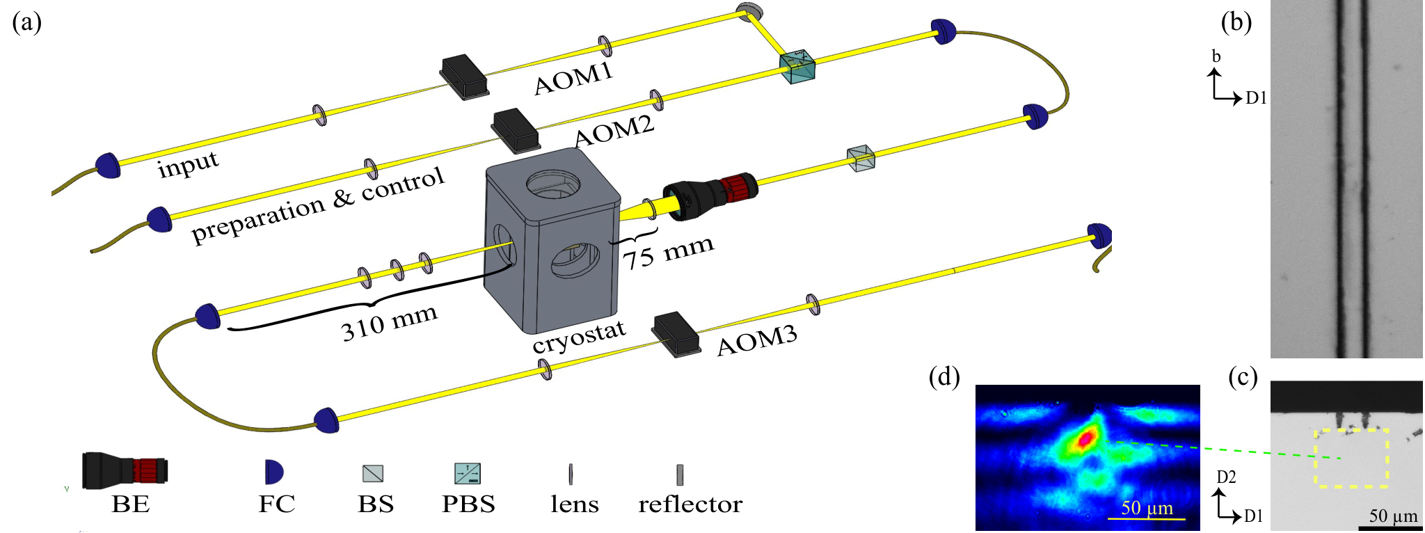
The waveguides fabricated by FLM are classified according to the refractive index changes in the laser-written area, geometric shape and waveguide position of the sample Chen and de Aldana 2014. The type-IV waveguide consists of two deep laser-irradiated scores and is located on the surface of the crystal; it is also called as the ridge waveguide. The laser beam can be constrained between the two gaps and propagates through the waveguide.
We use the FLM system from WOPhotonics (Altechna RD Ltd, Lithuania) to fabricate the type-IV waveguide on a : crystal, which has a doping level of 0.1% and a dimension of 10 mm 3.25 mm3.25 mm (). Many parameters affect the results of the fabrication processes, for instance, the wavelength, the pulse duration, the polarization, the repetition frequency, the waist size of the focus spot, and the energy of per pulse of the femtosecond laser Corrielli et al. 2016; Seri et al. 2018. Considering the anisotropy of the : crystal, the injection direction of the laser beam also influences the results of FLM Seri et al. 2018; Liu et al. 2020. In our experiment, the femtosecond laser beam is focused on the surface of the crystal by a objective whose numerical aperture is 0.4. The laser beam injects along the axis of the crystal and moves along the b axis with a speed of 1 mm/s. The distance between the two parallel damage tracks is set as 20 m. By optimizing the single-mode coupling efficiency of the 580-nm laser polarized along the axis in type-IV waveguides fabricated with various conditions, we obtain the following parameters: 1030 nm laser wavelength with 300 fs pulse duration, 20 kHz repetition rate, 1.7 J per-pulse energy and the polarization of the laser along the axis. The guided mode is bound by two ridges and the upper surface of the crystal. Since the defects on the crystal also affect the performance of FLM Liu et al. 2020, we fabricate several type-IV waveguides in the : crystal, in order to find a high-quality waveguide to conduct the experiments. The direct transmission (include coupling mode mismatch, waveguide propagation loss and Fresnel losses) of the waveguide is 19.4%. The coupling efficiency of the waveguide output into the single-mode fiber is 54%. The full width at half maximum (FWHM) of the guided mode is about 33 m 30 m (horizontal vertical) at the exit surface of the crystal, as shown in Fig. 1(d).

III EXPERIMENT SETUP
The laser source is a frequency-doubled semiconductor laser at 580 nm (TA-SHG, Toptica). The laser is locked to a stabilized Fabry-Perot (FP) cavity using the Pound-Drever-Hall technique Black 2001. The FP cavity is constructed from ultra-low expansion glasses and has a linewidth of 50 kHz. The locked laser has a linewidth of the order of 0.1 kHz. We use the AOMs and an arbitrary waveform generator to modulate and control the laser beam. As shown in Fig. 1, AOM1 and AOM2 are used to modulate the input mode and preparation and control mode, respectively. The sample is assembled on a cryostat (Montana Instruments) that can provide an environment of low vibration and a base temperature of approximately 3.2 K. Besides, a piezo-actuated three-axis stage is installed on the cryostat and its accuracy is of the order of 10 nm, which makes it convenient to couple the laser beam into the waveguides.
IV RESULT
IV.1 Characterization of the type-IV waveguide
To check whether the optical properties of the type-IV waveguide are modified as compared to those of the bulk area, we first measure the optical inhomogeneous broadening of the optical transition () of ions in different sections of the crystal. We choose three representative positions of the crystal, including the type-IV waveguide region, the bulk section at the same depth (13 m) beneath the upper surface of the crystal as the waveguide region (marked as bulk 1), and the bulk section at the center region, which is 1.6 mm beneath the top surface of the crystal (marked as bulk 2). We scan the frequency of incident light to obtain the absorption spectrum of the sample. The measured peak absorption frequency of bulk 1 is GHz and its FWHM is GHz; the peak absorption frequency of bulk 2 is GHz and its FWHM is GHz. These results indicate that the near-surface section of the crystal has the same optical inhomogeneous broadening as the center section of the crystal. The peak absorption frequency of the waveguide region is GHz and its FWHM length is GHz. The maximum absorption frequency of the waveguide has a red shift of 400 MHz compared to that of the two bulk sections and the linewidth is slightly broadened by 500 MHz.
The optical coherence time () is another important parameter to characterize the coherent properties of the type-IV waveguide. Two-pulse photon echo Tittel et al. 2010 experiments are implemented in the three representative regions (the type-IV waveguide area, bulk-1 area and bulk-2 area) of the sample. In Fig. 2 we shows the two-pulse photon echo amplitude as a function of the two-pulse spacing; the optical coherence time () is extracted from the inverse of the slope of the fitted curve. In the type-IV waveguide, we get of s when the peak power of the input pulse is 1.8 mW. The is s in the bulk 1 area and s in the bulk 2 area, with the peak power of the input pulse 4.7 and 4.6 mW, respectively. When testing in the bulk-1 and the bulk-2 areas, the input mode is the same as the optical mode coupling into the waveguide and has a FWHM of 7 m in the input surface of the crystal. The obtained for the waveguide region is essentially the same as that measured in the bulk regions. Therefore, we conclude that the fabrication process of the type-IV waveguide has negligible effects on the optical coherent properties of the sample, and this on-chip waveguide is ready for use as an optical quantum memory. The value reported here is partially limited by the “instantaneous spectral diffusion” because of the nonvanishing excitation Könz et al. 2003. Furthermore, the sample temperature may be slightly higher than expected since the sample is loosely connected to the cold finger to avoid any damage to the surface waveguide.
IV.2 Optical storage based on the type-IV waveguide
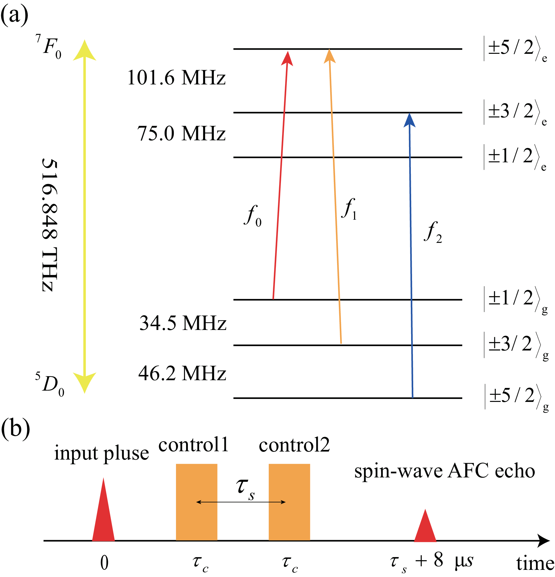
The AFC scheme is a widely employed quantum memory scheme in the solid-state system with the advantages of large bandwidth Usmani et al. 2010; Saglamyurek et al. 2011; Saglamyurek et al. 2016; Zhong et al. 2017a, high multimode capacity De Riedmatten et al. 2008; Usmani et al. 2010; Sinclair et al. 2014; Tang et al. 2015; Seri et al. 2017; Yang et al. 2018; Seri et al. 2019, long-lived coherence Zhong et al. 2015; Laplane et al. 2017; Rančić et al. 2018, and high storage fidelity De Riedmatten et al. 2008; Zhou et al. 2012; Jin et al. 2015; Zhou et al. 2015; Zhong et al. 2017a. Taking advantage of the large inhomogeneous broadening of the optical transition () of ions, a comb structure can be shaped on the spectrum by utilizing a spectral-hole burning technique Timoney et al. 2013. The periodicity of the comb is denoted by . When an optical pulse is absorbed by ions in the AFC at the initial moment, those ions with a detuning of will be collectively excited where is an integer. During the dephasing of the excited ions, a coherent AFC photon echo emits at time Afzelius et al. 2009. Long storage time and on-demand retrieval can be achieved by further utilizing the spin-wave AFC scheme Timoney et al. 2013. The core of this method is utilizing a control pulse to transfer the ions from the excited state into the extra empty ground state that freezes the AFC evolution and suppresses the two-level AFC echo. Then, another control pulse is applied to bring back the excitation. The rephasing process of the AFC scheme will continue and emit an echo (the so-called spin-wave AFC echo). The total storage time of the spin-wave AFC memory is with the time spacing between the two control pulses.
The level structure of the ions in the crystal is shown in Fig. 3. We utilize the spectral hole-burning process Liu et al. 2020; Lauritzen et al. 2012; Jobez et al. 2016 to prepare an AFC comb structure inside the waveguide, including class cleaning, population polarization, and creating the AFC structure at while keeping empty. The details of the preparation process can be found in our recent work Liu et al. 2020. As shown in Fig. 4, the prepared AFC has a bandwidth of 2 MHz and the measured internal efficiency of the AFC echo is 2.4% at a storage time of 8 s, which is calculated as the ratio between the intensity of the AFC echo and the input pulse. The theoretical AFC storage efficiency De Riedmatten et al. 2008 as estimated from the AFC structure shown in Fig. 4(b) is 2.4% which agrees with the measured value. The storage efficiency is primarily limited by the low absorption of the sample since the dopant has two natural isotopes ( and ) and only is employed here. At time , an input pulse with a frequency of and FWHM of 750 ns is injected into the type-IV waveguide and its AFC echo appears after 8 s. Next, two control pulses with a center frequency of and a chirp bandwidth of 2 MHz are applied to implement the spin-wave AFC scheme. The peak power of the control pulses is 58 mW before the cryostat and they each have a duration () of 2.5 s. The required power of the control pulses is approximately 10 times lower than that required in the bulk material Jobez et al. 2015. The estimated transfer efficiency of a single control pulse is approximately 50%. The spin-wave echo appears at s. The peak power of the input pulse is 5.8 mW before the cryostat in spin-wave storage and the internal efficiency of the 10.5 s spin-wave AFC storage is 0.5% inside the waveguide.

Because of the spin dephasing, the spin-wave AFC echo decays when increases. As shown in Fig. 4(c), the spin-wave AFC echo amplitude can be linear fitted with storage time in the spin state () on a log scale, which indicates a Lorentzian profile of the spin inhomogeneous broadening for Beavan 2012; Serrano et al. 2018. The echo amplitude () can be represented by
| (1) |
where is the inhomogeneous linewidth of the spin transition and is the spin-wave AFC echo amplitude with . The is fitted as kHz in our type-IV waveguide. The spin inhomogeneous broadening of ions inside the type-IV waveguide is approximately unchanged as compared to what is usually measured in the bulk region of a similar crystal Jobez et al. 2015, showing that the spin transition is also well protected in the waveguide fabrication process.
To characterize the fidelity of the entire storage process, we implement an interference test between the spin-wave AFC echo and a coherent reference pulse. The reference pulse is tuned precisely to overlap with the readout echo in the time domain Lovrić et al. 2013; Liu et al. 2020. Meanwhile, the relative phase between the signal pulse and the reference pulse is modulated to obtain the interference curve. The interference between them is detected using a calibrated photomultiplier tube Liu et al. 2020. We used the same AFC preparation sequence, input pulse and control pulse as the previous experiment. We set s and record the signal when increasing the relative phase with a step of 30 degrees. The results are shown in Fig. 5 with a fitted interference visibility of . This high visibility demonstrates the reliability of the on-chip optical memory in coherent phase storage. The remaining imperfection is mainly attributed to the imperfection of waveform overlap between the signal and reference pulses and the detector noise.

V CONCLUSION
A laser-written on-chip type-IV waveguide is fabricated on a : crystal. Coherent optical storage based on the spin-wave AFC scheme is implemented with high fidelity. The fabrication of the type-IV waveguide slightly shifts the absorption center and expands the optical inhomogeneous broadening, while the optical coherence time is unchanged during the fabrication. The spin inhomogeneous broadening of ions inside the type-IV waveguide is approximately unchanged as compared to what is usually measured in the bulk region of a similar crystal Jobez et al. 2015. This is in contrast to the type-II waveguide fabricated in : that introduces a significant broadening of both the optical transition and the spin transition Liu et al. 2020. This can be explained by the fact that the fabrication process of the type-IV waveguide is less damaging to the crystal than that of the type-II waveguide.
Because of its on-chip structure, the type-IV waveguide has unique benefits for future practical applications. Nevertheless, several extensions of the current work can be considered. First, the coupling efficiency is currently limited by the rough edges of the ridges, which can be improved by using a higher magnification objective to increase the accuracy of FLM, constructing the new ridges by multiple micromachinings at different depths under low per-pulse energy, or using ion-beam sputtering to reduce the roughness of the edges Chen and de Aldana 2014. Second, the spin-wave AFC scheme can be combined with dynamic decoupling to extend the storage lifetime Fraval et al. 2005; Jobez et al. 2015. By combining the type-IV waveguide with coplanar electrical waveguides, it is possible to achieve high-efficiency dynamical decoupling control with reduced radio-frequency power requirements. The efficient interface between such on-chip photonic memory and other on-chip photonic circuits should lead to versatile applications in large-scale quantum networks.
VI acknowledgments
This work is supported by the National Key R&D Program of China (Grant No. 2017YFA0304100), the National Natural Science Foundation of China (Grants No. 11774331, 11774335, No. 11504362, No. 11821404, and No. 11654002), the Anhui Initiative in Quantum Information Technologies (Grant No. AHY020100), the Key Research Program of Frontier Sciences, CAS (Grant No. QYZDY-SSW-SLH003), the Science Foundation of the CAS (Grant No. ZDRW-XH-2019-1), the Fundamental Research Funds for the Central Universities (Grants No. WK2470000026 and No. WK2470000029), and the Youth Innovation Promotion Association CAS.
References
- Lvovsky et al. (2009) A. I. Lvovsky, B. C. Sanders, and W. Tittel, Optical quantum memory, Nat. photonics 3, 706 (2009).
- Nunn et al. (2008) J. Nunn, K. Reim, K. C. Lee, V. O. Lorenz, B. J. Sussman, I. A. Walmsley, and D. Jaksch, Multimode memories in atomic ensembles, Phys. Rev. Lett. 101, 260502 (2008).
- Kok et al. (2007) P. Kok, W. J. Munro, K. Nemoto, T. C. Ralph, J. P. Dowling, and G. J. Milburn, Linear optical quantum computing with photonic qubits, Rev. Mod. Phys. 79, 135 (2007).
- Briegel et al. (1998) H.-J. Briegel, W. Dür, J. I. Cirac, and P. Zoller, Quantum repeaters: The role of imperfect local operations in quantum communication, Phys. Rev. Lett. 81, 5932 (1998).
- Sangouard et al. (2011) N. Sangouard, C. Simon, H. de Riedmatten, and N. Gisin, Quantum repeaters based on atomic ensembles and linear optics, Rev. Mod. Phys. 83, 33 (2011).
- De Riedmatten et al. (2008) H. De Riedmatten, M. Afzelius, M. U. Staudt, C. Simon, and N. Gisin, A solid-state light–matter interface at the single-photon level, Nature 456, 773 (2008).
- Wang et al. (2019) Y. Wang, J. Li, S. Zhang, K. Su, Y. Zhou, K. Liao, S. Du, H. Yan, and S.-L. Zhu, Efficient quantum memory for single-photon polarization qubits, Nat. Photonics 13, 346 (2019).
- Ritter et al. (2012) S. Ritter, C. Nölleke, C. Hahn, A. Reiserer, A. Neuzner, M. Uphoff, M. Mücke, E. Figueroa, J. Bochmann, and G. Rempe, An elementary quantum network of single atoms in optical cavities, Nature 484, 195 (2012).
- Chrapkiewicz et al. (2017) R. Chrapkiewicz, M. Dąbrowski, and W. Wasilewski, High-capacity angularly multiplexed holographic memory operating at the single-photon level, Phys. Rev. Lett. 118, 063603 (2017).
- Wallucks et al. (2020) A. Wallucks, I. Marinković, B. Hensen, R. Stockill, and S. Gröblacher, A quantum memory at telecom wavelengths, Nat. Phys. 16, 772 (2020).
- Usmani et al. (2010) I. Usmani, M. Afzelius, H. De Riedmatten, and N. Gisin, Mapping multiple photonic qubits into and out of one solid-state atomic ensemble, Nat. Commun. 1, 12 (2010).
- Saglamyurek et al. (2011) E. Saglamyurek, N. Sinclair, J. Jin, J. A. Slater, D. Oblak, F. Bussieres, M. George, R. Ricken, W. Sohler, and W. Tittel, Broadband waveguide quantum memory for entangled photons, Nature 469, 512 (2011).
- Saglamyurek et al. (2016) E. Saglamyurek, M. G. Puigibert, Q. Zhou, L. Giner, F. Marsili, V. B. Verma, S. W. Nam, L. Oesterling, D. Nippa, D. Oblak, et al., A multiplexed light-matter interface for fibre-based quantum networks, Nat. Commun. 7, 11202 (2016).
- Zhong et al. (2017a) T. Zhong, J. M. Kindem, J. Rochman, and A. Faraon, Interfacing broadband photonic qubits to on-chip cavity-protected rare-earth ensembles, Nat. Commun. 8, 14107 (2017a).
- Sinclair et al. (2014) N. Sinclair, E. Saglamyurek, H. Mallahzadeh, J. A. Slater, M. George, R. Ricken, M. P. Hedges, D. Oblak, C. Simon, W. Sohler, et al., Spectral multiplexing for scalable quantum photonics using an atomic frequency comb quantum memory and feed-forward control, Phys. Rev. Lett. 113, 053603 (2014).
- Tang et al. (2015) J.-S. Tang, Z.-Q. Zhou, Y.-T. Wang, Y.-L. Li, X. Liu, Y.-L. Hua, Y. Zou, S. Wang, D.-Y. He, G. Chen, et al., Storage of multiple single-photon pulses emitted from a quantum dot in a solid-state quantum memory, Nat. Commun. 6, 8652 (2015).
- Laplane et al. (2017) C. Laplane, P. Jobez, J. Etesse, N. Gisin, and M. Afzelius, Multimode and long-lived quantum correlations between photons and spins in a crystal, Phys. Rev. Lett. 118, 210501 (2017).
- Kutluer et al. (2017) K. Kutluer, M. Mazzera, and H. de Riedmatten, Solid-state source of nonclassical photon pairs with embedded multimode quantum memory, Phys. Rev. Lett. 118, 210502 (2017).
- Seri et al. (2017) A. Seri, A. Lenhard, D. Rieländer, M. Gündoğan, P. M. Ledingham, M. Mazzera, and H. de Riedmatten, Quantum correlations between single telecom photons and a multimode on-demand solid-state quantum memory, Physical Review X 7, 021028 (2017).
- Yang et al. (2018) T.-S. Yang, Z.-Q. Zhou, Y.-L. Hua, X. Liu, Z.-F. Li, P.-Y. Li, Y. Ma, C. Liu, P.-J. Liang, X. Li, et al., Multiplexed storage and real-time manipulation based on a multiple degree-of-freedom quantum memory, Nat. Commun. 9, 3407 (2018).
- Seri et al. (2019) A. Seri, D. Lago-Rivera, A. Lenhard, G. Corrielli, R. Osellame, M. Mazzera, and H. de Riedmatten, Quantum storage of frequency-multiplexed heralded single photons, Phys. Rev. Lett. 123, 080502 (2019).
- Zhong et al. (2015) M. Zhong, M. P. Hedges, R. L. Ahlefeldt, J. G. Bartholomew, S. E. Beavan, S. M. Wittig, J. J. Longdell, and M. J. Sellars, Optically addressable nuclear spins in a solid with a six-hour coherence time, Nature 517, 177 (2015).
- Rančić et al. (2018) M. Rančić, M. P. Hedges, R. L. Ahlefeldt, and M. J. Sellars, Coherence time of over a second in a telecom-compatible quantum memory storage material, Nat. Phys. 14, 50 (2018).
- Zhou et al. (2012) Z.-Q. Zhou, W.-B. Lin, M. Yang, C.-F. Li, and G.-C. Guo, Realization of reliable solid-state quantum memory for photonic polarization qubit, Phys. Rev. Lett. 108, 190505 (2012).
- Jin et al. (2015) J. Jin, E. Saglamyurek, M. l. G. Puigibert, V. Verma, F. Marsili, S. W. Nam, D. Oblak, and W. Tittel, Telecom-wavelength atomic quantum memory in optical fiber for heralded polarization qubits, Phys. Rev. Lett. 115, 140501 (2015).
- Zhou et al. (2015) Z.-Q. Zhou, Y.-L. Hua, X. Liu, G. Chen, J.-S. Xu, Y.-J. Han, C.-F. Li, and G.-C. Guo, Quantum storage of three-dimensional orbital-angular-momentum entanglement in a crystal, Phys. Rev. Lett. 115, 070502 (2015).
- Sinclair et al. (2010) N. Sinclair, E. Saglamyurek, M. George, R. Ricken, C. La Mela, W. Sohler, and W. Tittel, Spectroscopic investigations of a ti: Tm: Linbo3 waveguide for photon-echo quantum memory, J. Lumin. 130, 1586 (2010).
- Thiel et al. (2012) C. Thiel, Y. Sun, R. Macfarlane, T. Böttger, and R. Cone, Rare-earth-doped linbo3 and ktiopo4 (ktp) for waveguide quantum memories, J. Phys. B: At. Mol. Opt. Phys. 45, 124013 (2012).
- Liu et al. (2012) H. Liu, Y. Jia, J. R. V. de Aldana, D. Jaque, and F. Chen, Femtosecond laser inscribed cladding waveguides in nd:yag ceramics: Fabrication, fluorescence imaging and laser performance, Opt. Express 20, 18620 (2012).
- Corrielli et al. (2016) G. Corrielli, A. Seri, M. Mazzera, R. Osellame, and H. de Riedmatten, Integrated optical memory based on laser-written waveguides, Phys. Rev. Appl. 5, 054013 (2016).
- Seri et al. (2018) A. Seri, G. Corrielli, D. Lago-Rivera, A. Lenhard, H. de Riedmatten, R. Osellame, and M. Mazzera, Laser-written integrated platform for quantum storage of heralded single photons, Optica 5, 934 (2018).
- Liu et al. (2020) C. Liu, Z.-Q. Zhou, T.-X. Zhu, L. Zheng, M. Jin, X. Liu, P.-Y. Li, J.-Y. Huang, Y. Ma, T. Tu, et al., Reliable coherent optical memory based on a laser-written waveguide, Optica 7, 192 (2020).
- Marzban et al. (2015) S. Marzban, J. G. Bartholomew, S. Madden, K. Vu, and M. J. Sellars, Observation of photon echoes from evanescently coupled rare-earth ions in a planar waveguide, Phys. Rev. Lett. 115, 013601 (2015).
- Zhong et al. (2017b) T. Zhong, J. M. Kindem, J. G. Bartholomew, J. Rochman, I. Craiciu, E. Miyazono, M. Bettinelli, E. Cavalli, V. Verma, S. W. Nam, et al., Nanophotonic rare-earth quantum memory with optically controlled retrieval, Science 357, 1392 (2017b).
- Perry et al. (1999) M. Perry, B. Stuart, P. Banks, M. Feit, V. Yanovsky, and A. Rubenchik, Ultrashort-pulse laser machining of dielectric materials, Journal of applied physics 85, 6803 (1999).
- Gattass and Mazur (2008) R. R. Gattass and E. Mazur, Femtosecond laser micromachining in transparent materials, Nat. Photonics 2, 219 (2008).
- Skryabin et al. (2020) N. Skryabin, A. Kalinkin, I. Dyakonov, and S. Kulik, Femtosecond laser written depressed-cladding waveguide 2 2, 1 2 and 3 3 directional couplers in : crystal, Micromachines 11, 1 (2020).
- Chen and de Aldana (2014) F. Chen and J. V. de Aldana, Optical waveguides in crystalline dielectric materials produced by femtosecond-laser micromachining, Laser Photonics Rev. 8, 251 (2014).
- Kindem et al. (2020) J. M. Kindem, A. Ruskuc, J. G. Bartholomew, J. Rochman, Y. Q. Huan, and A. Faraon, Control and single-shot readout of an ion embedded in a nanophotonic cavity, Nature 580, 201 (2020).
- Turduev et al. (2018) M. Turduev, E. Bor, C. Latifoglu, I. H. Giden, Y. S. Hanay, and H. Kurt, Ultracompact photonic structure design for strong light confinement and coupling into nanowaveguide, J. Light. Technol. 36, 2812 (2018).
- Black (2001) E. D. Black, An introduction to pound–drever–hall laser frequency stabilization, Am. j. phys. 69, 79 (2001).
- Tittel et al. (2010) W. Tittel, M. Afzelius, T. Chaneliere, R. L. Cone, S. Kröll, S. A. Moiseev, and M. Sellars, Photon-echo quantum memory in solid state systems, Laser Photonics Rev. 4, 244 (2010).
- Könz et al. (2003) F. Könz, Y. Sun, C. W. Thiel, R. L. Cone, R. W. Equall, R. L. Hutcheson, and R. M. Macfarlane, Temperature and concentration dependence of optical dephasing, spectral-hole lifetime, and anisotropic absorption in :, Phys. Rev. B 68, 085109 (2003).
- Timoney et al. (2013) N. Timoney, I. Usmani, P. Jobez, M. Afzelius, and N. Gisin, Single-photon-level optical storage in a solid-state spin-wave memory, Phys. Rev. A 88, 022324 (2013).
- Afzelius et al. (2009) M. Afzelius, C. Simon, H. de Riedmatten, and N. Gisin, Multimode quantum memory based on atomic frequency combs, Phys. Rev. A 79, 052329 (2009).
- Lauritzen et al. (2012) B. Lauritzen, N. Timoney, N. Gisin, M. Afzelius, H. de Riedmatten, Y. Sun, R. M. Macfarlane, and R. L. Cone, Spectroscopic investigations of : for quantum memory applications, Phys. Rev. B 85, 115111 (2012).
- Jobez et al. (2016) P. Jobez, N. Timoney, C. Laplane, J. Etesse, A. Ferrier, P. Goldner, N. Gisin, and M. Afzelius, Towards highly multimode optical quantum memory for quantum repeaters, Phys. Rev. A 93, 032327 (2016).
- Jobez et al. (2015) P. Jobez, C. Laplane, N. Timoney, N. Gisin, A. Ferrier, P. Goldner, and M. Afzelius, Coherent spin control at the quantum level in an ensemble-based optical memory, Phys. Rev. Lett. 114, 230502 (2015).
- Beavan (2012) S. Beavan, Photon-echo rephasing of spontaneous emission from an ensemble of rare-earth ions, Ph.D. thesis, Laser Physics Centre, Research School of Physics and Engineering, The Australian National University (2012).
- Serrano et al. (2018) D. Serrano, J. Karlsson, A. Fossati, A. Ferrier, and P. Goldner, All-optical control of long-lived nuclear spins in rare-earth doped nanoparticles, Nat. Commun. 9, 2127 (2018).
- Lovrić et al. (2013) M. Lovrić, D. Suter, A. Ferrier, and P. Goldner, Faithful solid state optical memory with dynamically decoupled spin wave storage, Phys. Rev. Lett. 111, 020503 (2013).
- Fraval et al. (2005) E. Fraval, M. J. Sellars, and J. J. Longdell, Dynamic decoherence control of a solid-state nuclear-quadrupole qubit, Phys. Rev. Lett. 95, 030506 (2005).