Ultrathin perpendicular free layers for lowering the switching current in STT-MRAM
Abstract
The critical current density required for switching the magnetization of the free layer (FL) in a spin-transfer torque magnetic random access memory (STT-MRAM) cell is proportional to the product of the damping parameter, saturation magnetization and thickness of the free layer, . Conventional FLs have the structure CoFeB/nonmagnetic spacer/CoFeB. By reducing the spacer thickness, W in our case, and also splitting the single W layer into two layers of sub-monolayer thickness, we have reduced while minimizing and maximizing , ultimately leading to lower while maintaining high thermal stability. Bottom-pinned MRAM cells with device diameter in the range of 55–130 nm were fabricated, and is lowest for the thinnest (1.2 nm) FLs, down to 4 MA/cm2 for 65 nm devices, 30% lower than 1.7 nm FLs. The thermal stability factor , as high as 150 for the smallest device size, was determined using a domain wall reversal model from field switching probability measurements. With high and lowest , the thinnest FLs have the highest spin-transfer torque efficiency.
I Introduction
A leading challenge for the realization of a high-density STT-MRAM product is to have a low critical current required for switching the magnetization of the free layer, while maintaining high thermal stability for data retention. One route to reducing is to lower .Sun 2000 However, reducing is known to increase the temperature dependence of the magnetic anisotropy and thermal stability factor,Iwata-Harms et al. 2018 which leads to poor retention at elevated operating temperature. Rather than reducing , the approach taken in this study is to reduce while maximizing . Conventional free layers have the structure CoFeB/nonmagnetic spacer/CoFeB with a total thickness close to 2 nm. The role of the nonmagnetic spacer—typically metals such as Ta,W or Mo—is to absorb the boron atoms during the anneal step needed for solid-phase epitaxy of the MgO barrier and the CoFeB electrodes, which is critical for achieving high tunnel magnetoresistance (TMR)Butler et al. 2001; Mathon and Umerski 2001 and high interfacial perpendicular anisotropy.Sato et al. 2012a; Kim et al. 2015; Naik et al. 2012 The drawbacks for inserting these boron-sink materials are that they increase the damping constant of the FL, which is disadvantageous for lowering , and they create regions of low or zero moment in the free layer, referred to as a dead layer, which reduce volume-averaged .
In this study the strategy for increasing was to reduce the spacer thickness (and thus the dead layer) as much as possible, while still maintaining perpendicular anisotropy. Thicker CoFeB films need thicker spacer layers to stabilize perpendicular anisotropy. Hence, continuous reduction in spacer thickness necessitated a reduction in FL thickness. We found that thinner FLs with thinner spacer layers have higher . Our film characterization shows that FL properties improved by reducing down to 1.2 nm and splitting the single spacer layer into two thinner spacer layers. Our ultrathin FLs have reaching above 1700 emu/cm3 with no dead layer and with of only 0.003. We tested devices with in the range of 1.2–1.7 nm and device size down to 55 nm. Our device testing shows that is lower for the thinner FLs while the thermal stability factor for domain wall reversal remains high, so that overall there is an increase in spin-transfer torque efficiency, defined as where is the critical switching current.
II Experimental Method
The STT-MRAM stacks in this study consist of the following layer structure: bottom electrode/seed layer/CoFeB reference layer/MgO tunnel barrier/free layer/MgO cap/Ru/Ta/Ru top electrode. In these bottom-pinned stacks, a Co/Pt-based synthetic antiferromagnet (SAF) was used to pin the magnetization of the reference layer. These stacks were sputtered at room temperature using an Anelva-7100 system and then postannealed at 335∘C for 1 hour. The MgO layers were RF-sputtered from a MgO target.
In order to study the magnetic properties of the FL without any additional magnetic signal from the SAF or reference layer in the full STT-MRAM stack, the following FL-only stacks were prepared on oxidized Si substrates (thickness in nm): bottom electrode/3 Ta/5 Ru/0.3 W/0.5 CoFeB/1 MgO/FL/0.7 MgO/Ru. The 0.5 nm CoFeB seed layer is nonmagnetic at room temperature. The magnetic properties of the FL in the FL-only stack closely match those of the identical FL deposited in the bottom-pinned MRAM stack.
A FL thickness ladder of the following thicknesses were prepared: 1.2, 1.3, and 1.7 nm. For each thickness, two FL designs were compared: one with a single tungsten spacer (referred to as single-W) and the other with two tungsten spacers (referred to as split-W). For a given FL thickness, the combined W thickness of the two W layers in the split-W FL is equivalent to the thickness of the single W spacer in the single-W FL. The total W thickness is designated as . The single-W FLs have the following layer structure, listed in order as sputtered on top of the MgO barrier: CoFeB/CoFe/Mg/W/CoFe. The split-W FLs have the following layer structure: CoFeB/CoFe/Mg/W/CoFe/Mg/W/CoFe. Refer to Table 1 for the nominal thickness of every layer for each FL in this study. The Mg layers are sacrificial layers that protect the previously sputtered CoFe film from damage caused by the impinging W atoms during deposition of the W spacer, as described in Ref. Swerts et al. 2015. In agreement with Ref. Swerts et al. 2015, we have found that no Mg remains in the FL.11 1 As determined in a separate study of similar film stacks using cross-section transmission electron microscopy with elemental analysis using electron energy loss spectroscopy, in both the as-sputtered and post-annealed state The Mg thickness used here was determined by optimizing for highest of the free layer. and anisotropy field were determined from hard-axis magnetization versus magnetic field loops of unpatterned films measured by vibrating sample magnetometry (VSM).
| single-W | split-W | |||||||||||||
|---|---|---|---|---|---|---|---|---|---|---|---|---|---|---|
| CoFeB | CoFe | Mg | W | CoFe | CoFeB | CoFe | Mg | W | CoFe | Mg | W | CoFe | ||
| 1.22 | 0.04 | 0.47 | 0.31 | 1.00 | 0.04 | 0.40 | 0.47 | 0.11 | 0.60 | 0.02 | 0.26 | 0.60 | 0.02 | 0.34 |
| 1.20 | 0.015 | 0.47 | 0.31 | 1.00 | 0.015 | 0.40 | 0.47 | 0.11 | 0.60 | 0.008 | 0.26 | 0.60 | 0.007 | 0.34 |
| 1.30 | 0.04 | 0.52 | 0.32 | 1.00 | 0.04 | 0.42 | 0.52 | 0.10 | 0.60 | 0.02 | 0.32 | 0.60 | 0.02 | 0.32 |
| 1.70 | 0.12 | 0.73 | 0.32 | 1.00 | 0.12 | 0.53 | 0.73 | 0.11 | 0.60 | 0.06 | 0.37 | 0.60 | 0.06 | 0.37 |
The reported here is the nominal film thickness and includes the thickness of all the CoFeB, CoFe and W components. The nominal film thickness was determined using sputter time, and the sputter rate (i.e. nm/s) was calibrated for thick films using x-ray reflectivity. Thus, as the nominal W layer thickness is well below the thickness of a W atom, the W layer thickness refers to a partial monolayer of W atoms. As shown in the plot of saturation moment per area versus in Fig. 1a for our split-W free layer design with =0.04 nm, the linear fit line intersects the x-axis at 0 nm, indicating that there is no dead layer. A cross-section transmission electron micrograph (TEM) of the split-W FL-only film with =1.3 nm is shown in Fig. 1b. The 1.0 nm thick MgO barrier and the 0.7 nm MgO cap are easily identified, with the 1.3 nm free layer in between the MgO layers.

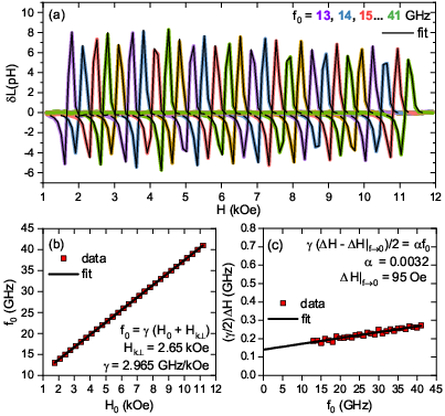
Vector network analyzer ferromagnetic resonance (VNA-FMR) measurements were performed on the unpatterned, FL-only films to determine the effective anisotropy field , the damping parameter , and inhomogeneous linewidth broadening . The applied field perpendicular to the film plane was swept once from 12 kOe to 1 kOe while transmission coefficients were simultaneously measured at 29 discrete frequencies in the range =13–41 GHz. See Fig. 2 for an example. Inhomogeneous broadening originates from non-uniformities of the anisotropy, and thus it is an indicator of film uniformity. Lower indicates better film uniformity.
Device performance was compared for the FLs in the thickness ladder, specifically the six free layers described in rows 2-4 of Table 1. Bottom-pinned STT-MRAM test devices were fabricated using 193 nm deep UV optical lithography, followed by reactive ion etching of a hard mask, ion milling of the MRAM film, SiO2 refill and then chemical mechanical planarization. Four different device sizes were fabricated for each FL, resulting in median electrical diameters in the range of 55 to 130 nm. Device diameter was determined from the measured device resistance in the parallel state and the resistance-area product , as . The product, along with TMR ratio, was measured using the current-in-plane-tunneling (CIPT) techniqueWorledge and Trouilloud 2003 on identical, unpatterned film stacks sputtered within the same batch as the device wafers.

To determine for the FLs in the devices, we measured empirical field-switching probability distributions , whereby 100 resistance versus field transfer loops were measured at low bias (10mV, to eliminate spin-transfer torque effects) using a staircase ramp with a field step of 5 Oe and a dwell time of 0.2 ms. An example is shown in Fig. 3a for a device with diameter 63 nm and split-W FL with =1.3 nm. Because the reversal mechanism for the FL magnetization in devices with diameters larger than 50 nm that we have studied here is by domain wall nucleation and propagation,Thomas et al. 2015; Chaves-O’Flynn et al. 2015 was fit using a domain wall reversal model.Mihajlović et al. An example of the fit is shown as black lines in Fig. 3b. The fit parameters are domain wall energy density and domain wall width , and is given as , where is the Boltzmann constant and is temperature. Using the following relations between and , we calculate exchange constant :
| (1) | |||
| (2) | |||
| (3) |
The was obtained by fitting the pulse width () dependence of switching voltage , measured in the range of 5 s - 5 ms as described in Ref. Mihajlović et al. 2020, to the thermal activation model for spin-transfer torque switching.Koch et al. 2004; Li and Zhang 2004 The switching voltage (defined at zero temperature and infinitely long time) is the intercept of the linear fit for versus , and .
III Results and Discussion
III.1 Film properties

We first compare the magnetic properties for a single-W FL and a split-W FL with the same nominal nm and nm. Figures 4a and 4e display the easy axis and hard axis loops, respectively, for the FLs described in the first row of Table 1. The split-W FL has a slightly higher and sharper switching (more square loop), as seen in the easy axis , and higher anistropy field, as seen in the hard axis . The and FMR results are listed in Table 2. Splitting the W spacer from a single 0.04 nm layer to two 0.02 nm layers resulted in an sizeable increase of from 3.02 kOe to 4.07 kOe and more than 3-fold reduction of , signifying a more uniform film. The low damping constant was maintained at .
It has been our observation that measured at the film level has a negative correlation to the coercive field at the device level; higher typically results in low , regardless of . Therefore, it is desireable to minimize as much as possible. In order to lower even further, we reduced the thickness of the W spacer. Figures 4b and 4f display the M(H) loops for the single-W and split-W FLs for which was reduced to 0.015 nm (refer to the second row in Table 1). As is typical when reducing the W spacer thickness, we observed higher , lower and lower , compared to the nm FLs. Importantly, there was another significant reduction of when going from single- to split-W spacers, dropping to 100 Oe which is promising for high at the device level.
| No. of | |||||||
|---|---|---|---|---|---|---|---|
| (nm) | (nm) | W layers | (emu/cm3) | (kOe) | (Oe) | (erg/cm) | |
| 1.22 | 0.04 | 1 | 1572 | 3.02 | 0.0040 | 420 | |
| 1.22 | 0.04 | 2 | 1644 | 4.07 | 0.0037 | 125 | |
| 1.20 | 0.015 | 1 | 1714 | 1.44 | 0.0036 | 210 | 1.7 |
| 1.20 | 0.015 | 2 | 1783 | 1.72 | 0.0031 | 80 | 2.01 |
| 1.30 | 0.04 | 1 | 1634 | 2.55 | 0.0037 | 180 | 1.77 |
| 1.30 | 0.04 | 2 | 1651 | 2.65 | 0.0032 | 95 | 1.85 |
| 1.70 | 0.12 | 1 | 1435 | 1.98 | 0.0044 | 95 | 1.49 |
| 1.70 | 0.12 | 2 | 1400 | 2.05 | 0.0044 | 85 | 1.47 |
For the =1.3 nm and 1.7 nm films in the FL thickness ladder of this study, the loops are displayed in Figures 4c,g and 4d,h, respectively, and the magnetic properties are listed in Table 2. Thicker FLs require more W in order to maintain perpendicular anisotropy, which results in lower . Therefore, is highest for the thinnest FLs. As demonstrated above, can be tuned by the W amount. The W amount used here is the minimum amount necessary to maintain perpendicular anisotropy. is significantly lower for the split-W FLs compared to the single-W FLs, with the exception of the 1.7 nm FLs, for which there appears to be no advantage to having two spacers as all parameters are nearly the same for the two designs. Noteably, contrary to the common observation that and increase for thin CoFeB,Liu et al. 2011; Sabino et al. 2014; Enobio et al. 2015 is very low for all of these ultrathin FLs, which is advantageous for achieving lower switching current.
III.2 Device Performance
The TMR for the six FLs is shown versus electrical diameter in Fig. 5a. This TMR measured for the devices closely matches the TMR values measured by CIPT (not shown). TMR is lower for the thinner FLs. In addition, TMR is lower for the split-W FLs. In general, lower TMR is observed for thinner free layers.Sato et al. 2012b; Cuchet et al. 2014 More specifically in our FLs, in the single-W FL stack as becomes thinner, the amount of CoFeB and CoFe between the MgO barrier and the W spacer becomes thinner, which means that the W atoms are closer to the MgO barrier. Any W atoms near the MgO/CoFeB interface are expected to disrupt the solid-phase epitaxy across this interface and thus disturb the coherent tunneling that otherwise generates high TMR.Butler et al. 2001 The W atoms are even closer to the MgO/CoFe interface in the case of the split-W FLs, which is thought to cause the TMR to be even lower.
The device coercivity (see Fig. 5b) is in the range of 2.2–2.6 kOe for the smallest device size for all FL designs, with the exception of the 1.2 nm single-W FL, which has the lowest film-level and highest .

The results of the field switching probability test with data fit to a domain wall reversal model is displayed in Figure 6a-c. The for all FLs is the range of 12–17 nm. The 1.2 nm and 1.3 nm split-W FLs have the highest . When multiplied by free layer volume to calculate , we find that all FLs, with the exception of the single-W 1.2 nm FL (having low ), have similarly high in the range of 130–150 for the smallest device size. Noteably, for the split-W FLs, we have reduced from 1.7 nm to 1.2 nm without significant loss of , while drops by a third with this reduction, as shown in Fig. 6d. Indeed, is lowest for the thinnest FLs with the split-W design, which have the lowest (refer to Table 2). Spin-transfer torque efficiency, defined as and shown in Fig. 6e, is highest for the thinnest FLs with the split-W design.
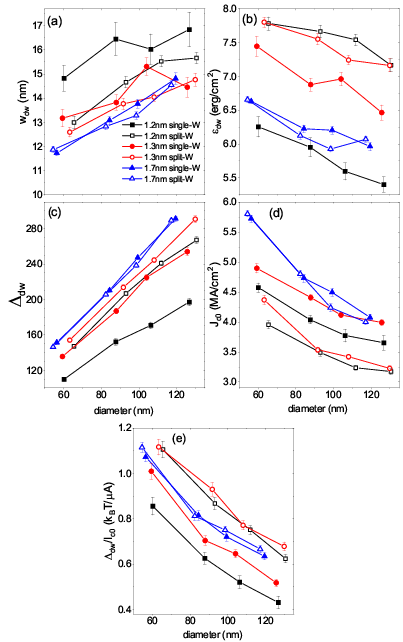
The for each FL calculated using Equation 3 is listed in Table 2. Overall, these values are high, approaching the values for bulk Fe (2.0 erg/cm) and confirming the high quality of the FLs, in agreement with the film-level characterization. These values are similar to deduced from spin-wave spectroscopy for perpendicular CoFeB free layers in nanopillar magnetic tunnel junctions.Helmer et al. 2010; Devolder et al. 2016 For the 1.2 nm and 1.3 nm FL thicknesses, is higher for the split-W FL compared to the single-W FL, consistent with the superior properties observed at the film level for the split-W design (refer to Table 2). Whereas for the two 1.7 nm FLs, the values are nearly the same, consistent with the other parameters for these films listed in Table 2. When comparing across the thickness ladder for the split-W FLs, we observe higher for thinner W spacer, in agreement with the trend observed with the film-level magnetometry measurements of Ref. Mohammadi et al. 2019 and magneto-optical Kerr microscopy studies of Ref. Buford et al. 2016.
As the film and device results for the 1.7 nm single-W and split-W FLs are the same, one may conclude that there is no advantage to splitting the single W spacer into two spacers for this FL thickness, and that this split-W approach is only beneficial for thinner FLs. However, only one 1.7 nm split-W FL was explored in this study. By varying the thickness of the CoFeB and CoFe layers below, between, and above the two W spacers, it may be possible to tune and to achieve a 1.7 nm split-W FL design with superior performance. This would suggest some sensitivity to the proximity of the two W spacers to the MgO interfaces and to each other. Of course, thicker CoFeB between the MgO barrier and W spacer is desireable for higher TMR.
Lastly, we did attempt to extend our multi-spacer design beyond two W spacers, but any higher number of spacers resulted in a steep degradation of film properties. It becomes more challenging to control the thickness of even thinner W layers and to optimize more Mg sacrificial layers. The extreme end of the multi-spacer approach is a CoFeBW alloy free layer, though this is likely to result in lower and lower Curie temperature.
IV Conclusions
In summary, by minimizing the W spacer thickness in the FL, we have eliminated the dead layer, thereby maximizing . We obtained optimal magnetic properties by splitting the W spacer layer into two thinner layers. For the FL thickness ladder in this study, from 1.2 nm to 1.7 nm, highest was obtained for the thinnest FLs, while maintaining low damping constant and low inhomogenous broadening of the FMR linewidth, signifying a more uniform and better quality film.
From device measurements, was highest for the thinnest FLs with split-W spacer, and thus high was maintained. We observed a thickness dependence of : the 1.2 nm FL has 30% lower than the 1.7 nm FL. The thinnest FLs with split-W spacer have the lowest and highest spin-transfer-torque efficiency.
Data Availability
The data that supports the findings of this study are available within the article.
Acknowledgements.
The authors acknowledge Michael Gribelyuk, Loc Vinh and Xiaoyu Xu at the Western Digital Materials Laboratory for providing the high-resolution TEM analysis.References
- Sun (2000) J. Z. Sun, Phys. Rev. B 62, 570 (2000).
- Iwata-Harms et al. (2018) J. M. Iwata-Harms, G. Jan, H. Liu, S. Serrano-Guisan, J. Zhu, L. Thomas, R.-Y. Tong, V. Sundar, and P.-K. Wang, Sci. Rep. 8, 14409 (2018).
- Butler et al. (2001) W. H. Butler, X.-G. Zhang, T. C. Schulthess, and J. M. MacLaren, Phys. Rev. B 63, 054416 (2001).
- Mathon and Umerski (2001) J. Mathon and A. Umerski, Phys. Rev. B 63, 220403(R) (2001).
- Sato et al. (2012a) H. Sato, M. Yamanouchi, S. Ikeda, S. Fukami, F. Matsukura, and H. Ohno, Appl. Phys. Lett. 101, 022414 (2012a).
- Kim et al. (2015) J.-H. Kim, J.-B. Lee, G.-G. An, S.-M. Yang, W.-S. Chung, H.-S. Park, and J.-P. Hong, Sci. Rep. 5, 16903 (2015).
- Naik et al. (2012) V. B. Naik, H. Meng, and R. Sbiaa, AIP Advances 2, 042182 (2012).
- Swerts et al. (2015) J. Swerts, S. Mertens, T. Lin, S. Couet, Y. Tomczak, K. Sankaran, G. Pourtois, W. Kim, J. Meersschaut, L. Souriau, D. Radisic, S. Van Elshocht, G. Kar, and A. Furnemont, Appl. Phys. Lett. 106, 262407 (2015).
- (9) As determined in a separate study of similar film stacks using cross-section transmission electron microscopy with elemental analysis using electron energy loss spectroscopy, in both the as-sputtered and post-annealed state.
- (10) N. Smith, unpublished .
- Worledge and Trouilloud (2003) D. C. Worledge and P. L. Trouilloud, App. Phys. Lett. 83, 84 (2003).
- (12) G. Mihajlović, N. Smith, T. Santos, J. Li, B. D. Terris, and J. A. Katine, arXiv:2008.00412 .
- Thomas et al. (2015) L. Thomas, G. Jan, S. Le, Y.-J. Lee, H. Liu, S. Zhu, J. Serrano-Guisan, R.-Y. Tong, K. Pi, D. Shen, R. He, J. Haq, Z. Teng, A. Rao, V. Lam, Y.-J. Wang, T. Zhong, T. Torng, and P.-K. Wang, 2015 IEEE International Electron Devices Meeting (IEDM) , 26.4.1 (2015).
- Chaves-O’Flynn et al. (2015) G. D. Chaves-O’Flynn, G. Wolf, J. Z. Sun, and A. D. Kent, Phys. Rev. Appl. 4, 024010 (2015).
- Mihajlović et al. (2020) G. Mihajlović, N. Smith, T. Santos, J. Li, M. Tran, M. Carey, B. Terris, and J. Katine, Phys. Rev. Appl. 13, 024004 (2020).
- Koch et al. (2004) R. H. Koch, J. A. Katine, and J. Z. Sun, Phys. Rev. Lett. 92, 088302 (2004).
- Li and Zhang (2004) Z. Li and S. Zhang, Phys. Rev. B 69, 134416 (2004).
- Liu et al. (2011) X. Liu, W. Zhang, M. J. Carter, and G. Xiao, J. Appl. Phys. 110, 033910 (2011).
- Sabino et al. (2014) M. P. R. Sabino, S. T. Lim, and M. Tran, IEEE Trans. Magn. 50, 6101404 (2014).
- Enobio et al. (2015) E. C. I. Enobio, H. Sato, S. Fukami, F. Matsukura, and H. Ohno, IEEE Mag. Lett. 6, 5700303 (2015).
- Sato et al. (2012b) H. Sato, M. Yamanouchi, K. Miura, S. Ikeda, R. Koizumi, F. Matsukura, and H. Ohno, IEEE Magn. Lett. 3, 3000204 (2012b).
- Cuchet et al. (2014) L. Cuchet, B. Rodmacq, S. Auffret, R. Sousa, and B. Dieny, Appl. Phys. Lett. 105, 052408 (2014).
- Helmer et al. (2010) A. Helmer, S. Cornelissen, T. Devolder, J.-V. Kim, W. van Roy, L. Lagae, and C. Chappert, Phys. Rev. B 81, 094416 (2010).
- Devolder et al. (2016) T. Devolder, J.-V. Kim, L. Nistor, R. Sousa, B. Rodmacq, and B. Diény, J. Appl. Phys. 120, 183902 (2016).
- Mohammadi et al. (2019) J. B. Mohammadi, B. Kardasz, G. Wolf, Y. Chen, M. Pinarbasi, and A. D. Kent, ACS Appl. Electron. Mater. 1, 2025 (2019).
- Buford et al. (2016) B. Buford, P. Dhagat, and A. Jander, IEEE Magn. Lett. 7, 3107903 (2016).