Fullwave Maxwell inverse design of axisymmetric, tunable, and multi-scale multi-wavelength metalenses
Abstract
We demonstrate new axisymmetric inverse-design techniques that can solve problems radically different from traditional lenses, including reconfigurable lenses (that shift a multi-frequency focal spot in response to refractive-index changes) and widely separated multi-wavelength lenses (m and m). We also present experimental validation for an axisymmetric inverse-designed monochrome lens in the near-infrared fabricated via two-photon polymerization. Axisymmetry allows fullwave Maxwell solvers to be scaled up to structures hundreds or even thousands of wavelengths in diameter before requiring domain-decomposition approximations, while multilayer topology optimization with degrees of freedom can tackle challenging design problems even when restricted to axisymmetric structures.
I Introduction
In this paper, we demonstrate that axisymmetric metalenses can be designed with fullwave Maxwell simulations (as opposed to the scalar-diffraction meem2020large or domain-decomposition approximations pestourie2018inverse used in prior metasurface designs), for wavelengths () in diameters, combined with multilayer variable-height topology optimization (TO) with degrees of freedom ( per per layer) as shown in Fig. 1. The capability and flexibility of our design approach is demonstrated by solving two challenging new design problems with 10-layer metalenses. First (in Sec. III), we design a multi-scale metalens that simultaneously focuses m and m at the same diffraction-limited focal point (numerical aperature NA , Strehl ratios of and and efficiencies of % and %, respectively). Second (in Sec. IV), we design an active metalens that shifts its achromatic multi-wavelength (three s over a 6% bandwidth) focal spot from NA to as the index of the material (GSS4T1 ZHANG_ET_AL_2019) is changed from to (thermally or optically), in contrast to previous work that showed only monochromatic reconfigurability shalaginov2019reconfigurable. As a proof of concept, we also show (in Sec. V) an experimental realization of single-layer axisymmetric TO-designed metalens for nm, fabricated by two-photon polymerization 3D-printing (Nanoscribe Professional GT), demonstrating that such variable-height surfaces are manufacturable. As discussed in Sec. VI, our approach could easily be scaled to much larger diameters and number of layers, and the vast number of design degrees of freedom coupled with the lack of approximations makes it a uniquely attractive method for the most difficult metasurface inverse designs.
Flat-optics metalenses have received widespread attention due to their potential for achieving multiple functionalities within an ultra-compact form factor yu2014flat; khorasaninejad2016metalenses; khorasaninejad2017metalenses; aieta2015multiwavelength; chen2018broadband. Prior work on metalens design has largely focused on exploiting local resonant conditions yu2014flat under locally periodic approximation (LPA), using rather small unit cells () pestourie2018inverse; lin2019topology. Recently, it has been shown that the unit-cell approach with LPA can lead to fundamental limitations on metalens performance chung2020high; presutti2020focusing, whereas some of these limitations may be mitigated by using overlapping boundaries, perfectly matched layers or larger domains lin2019overlapping; phan2019high some may not. Meanwhile, axisymmetric multi-level diffractive lenses (MDL) have been proposed as an alternative to metalenses for achieving enhanced functionalities BANERJI_ET_AL_2019; meem2020imaging; however, MDL designs utilize scalar diffraction theory subject to locally uniform approximation, neglecting multiple scatterings or resonant phenomena, and, thus, have limited design complexity and physical behavior engelberg2020advantages. In contrast to previous works, our approach considers axisymmetric multilayered freeform metalenses which can be modelled by rigorous fullwave Maxwell equations without any uncontrolled approximations.
The prospect of fabricating single-layer metasurfaces with traditional single-step lithography processes is very promising for large-scale high-throughput integration khorasaninejad2016metalenses; khorasaninejad2017metalenses. However, single-layer metasurfaces have been limited in their functionality to narrow angular and spectral bandwidths of operation, with some progress towards chromatic chen2018broadband and geometrical aberration correction groever2017meta. Achieving truly multifunctional metasurfaces requires more advanced designs, such as closely-packed multilayer structures lin2018topology; lin2019topology; lin2019overlapping; chung2020high. Recently, there has been a surge in interest in fabricating multilayer metasurfaces mansouree2020multifunctional; zhou2018multilayer, bolstered by advances in inverse-designed nanophotonics. However, these designs can only be fabricated with more advanced fabrication techniques, such as multi-step lithography, or multi-photon lithography. Multi-photon lithography/polymerization is a technique that enables the fabrication of sub-micron (down to 150 nm) arbitrary three-dimensional structures. Two-photon polymerization enabled the demonstration of three-dimensional chiral/helical structures gansel2009gold; wu20193d and was more recently applied to the fabrication of supercritical lenses fang2020multilevel; coompson20183d and to the demonstration of full three dimensional control of optical fields using a metasurface ZHAN_ET_AL_2019. Nonetheless, the possibility of 3D printing inverse-designed metasurfaces with two-photon lithography processes remains largely unexplored. In this work, we realize a proof-of-concept experiment with an inverse-designed, freeform, single-layer metalens working at nm fabricated via two-photon polymerization.
The use of TO as a tool for inverse design in nanophotonics has increased steadily over the last two decades JENSEN_SIGMUND_2011; MOLESKY_2018 with a recent application to metalens design lin2018topology. Our proposed multilayer metalens design framework utilizes density-based topology optimization BOOK_TOPOPT_BENDSOE as the inverse design tool. Rather than allowing fully free-form 3D designs, not amenable to nano-scale fabrication, we propose using TO to control the radial height-variation of the -layers constituting the lens. In addition, we propose using a filtering technique BOURDIN_2001; LAZAROV_2011 combined with a threshold operation to limit the gradient of the height variations, making it possible to ensure that they comply with fabrication constraints.

II Model and design problem
The design problem is modelled in an axisymmetric domain, , sketched in Fig. 1A(right). The model domain contains a designable region, (gray), where the metalens is placed on a solid material surface (dark gray). The sketch also indicates the plane, (magenta line), used for computing the far-field transformation in Eq. 1, the focal plane(s), (blue and red lines), and the focal spot(s), (black dots), of the lens. Finally, the model domain is truncated using a perfectly matching layer in BERENGER_1994; CHEW_1997. The lens-design itself consists of layers of material (Fig. 1A(left)), each with a variable height controlled by the design field, . Each designable layer is separated from the next by a layer of air (light gray) and a layer of solid material (dark gray) of fixed thicknesses.
The physics is modelled in using the Maxwell Equations BOOK_EM_GRIFFITHS assuming time-harmonic behavior. Doing so, we capture the full-wave behavior of the electromagnetic field without simplifying assumptions, thus enabling the exploitation of the full-wave behavior to design metalenses exerting precise control of the electromagnetic field. To make the model problem numerically tractable for large design domains, we assume an axisymmetric geometry. This enables the reduction of the full 3D Maxwell Equations to their 2D axisymmetric counterparts BOOK_FEM_EM_JIN, therefore significantly reducing the computational effort required to solve the model problem at the cost of a geometric restriction on the design.
The model problem is solved using the scattered-field formulation, , where the background field, , is taken to be a planewave propagating along the z-axis (decomposed into two counter-rotating circularly polarized waves). The model problem is discretized using the Finite Element Method (FEM) BOOK_FEM_EM_JIN and solved using COMSOL Multiphysics v5.5 COMSOL55.
A far-field transformation taflove2005computational may be used to compute the electric field at any point in space given knowledge of the field in the plane above the lens, see Fig. 1. The use of this transformation removes the need for simulating the spatial domain between the lens and focal point, hereby significantly reducing computational cost. The far field transformation may be written as,
| (1) |
Here denotes the electric far field at the point r, and denotes the electric and magnetic field Green’s functions, respectively. Finally and denote the equivalent magnetic and electric surface currents computed from the electric and magnetic near field obtained by solving the model problem.
The figure of merit (FOM) used in the design process is the electric field-intensity at the focal point, . The design problem is formulated as the following continuous constrained optimization problem,
| (2) | |||||
| (3) |
Here denotes a radially-varying design field, which controls the thickness of the ’th layer of the metalens. The electric field at the focal point, , is computed using the solution to the physical model problem and Eq. 1.
We propose using a standard PDE-filter LAZAROV_2011 to limit the layer-thickness gradient, by applying it to through the choice of filter radius, . After filtering we propose using to control the layer height through the smoothed threshold operation WANG_ET_AL_2011 as,
| (4) |
Here denotes the spatial position inside each designable layer. The value corresponds to the bottom of the designable region in the ’th layer, and the value corresponds to the top of the designable region in the ’th layer. The threshold sharpness is controlled by . In the limit of the field takes the value 0 when and the value 1 when . A continuation approach may be used to gradually increase during the inverse design process to enforce a 0/1 final design.
The field is used to interpolate the relative permittivity, , in space between the background material and the material constituting the metalens using a linear scheme,
| (5) |
Here (resp. ) denotes the relative permittivity of the background (resp. lens).
The design problem, Eqs. (2-3), is solved using the Method of Moving Asymptotes SVANBERG_2002, for which the sensitivites of the FOM are computed using adjoint sensitivity analysis TORTORELLI_ET_AL_1994. Details regarding the modelling and optimization process as well as the parameter choices for each example are found in Appendix A and Appendix B, respectively.
The final designs are all evaluated numerically using a high resolution model by exciting the lens using a linearly polarized planewave decomposed into two counter-rotating circularly polarized waves introduced in the model using a first order scattering boundary condition. An example of a reconfigurable metalens operating at m for two different refractive indices is shown in Fig. 1B.
III Multi-scale multi-wavelength multilayer metalens
As the first example of our framework we tailor a 10-layer silicon () in air metalens to focus m light (Fig. 2A) and m light (Fig. 2B) simultaneously at the same focal spot (NA). The lens is 100 m in diameter and has a thickness of 10 m. The inverse-designed lens is presented in Fig. 2E with the insert showing an example of the layer-height variations.

From Fig. 2A-2B it is clear that the lens exhibits the desired numerical aperture (green line). The focusing capability of the lens is found to reach the diffraction-limit for both wavelengths, when measured in terms of the Full Width at Half Maximum (FWHM) of the main lobe in the focal plane (Fig. 2C-2D). The Strehl ratio (SR) at the two targeted wavelengths, m and m, is computed to be SR and SR , respectively. The SR is computed based on the power flow through the focal plane (blue lines) and the corresponding Airy discs (dashed red lines), shown in Fig. 2C-2D. The absolute power transmission from the substrate of silicon through the lens is computed to be and , relative to the incident power in the silicon substrate within the lens diameter. Appendix C includes an additional design example targeting NA rather than NA= while keeping all other parameters fixed, demonstrating the methods versatility. For that second example we also achieve diffraction-limited focusing and attain Strehl ratios of SR and SR for m and m, respectively.
To illustrate the benefit of the proposed multi-layer metalens over a single-layer lens we consider a simple single-layer reference design (Fig. 2F). The single-layer design is optimized using our proposed approach, with all parameters used in the example held constant, except for the number of layers. For this single-layer reference design we obtain a Strehl Ratio of and and an absolute transmission efficiency of and at and , respectively. Comparing the Strehl ratios and absolute transmission efficiencies to those obtained for the ten layer metalens design, the benefit of multi-layer metalens designs over single-layer designs for this example is clear.
IV Tunable multi-wavelength multilayer metalens
As a second example of our framework, we design of a 10-layer tunable three-wavelength metalens (see Fig. 1C) capable of shifting the numerical aperture of the lens from NA (see Fig. 3[Left Column]) to NA (see Fig. 3[Right Column]) by changing the refractive index of the active material (GST41T1 ZHANG_ET_AL_2019) from to .

The lens is 625 m in diameter and has a thickness of 25 m. The lens is designed to operate in the mid-infrared region at wavelengths, m (Fig. 3[Row 1]), m (Fig. 3[Row 2]) and m (Fig. 3[Row 3]). From Fig. 3 it is observed that the lens exhibits the desired numerical aperture at all three wavelengths for both values of the refractive index. The Strehl ratio, absolute power transmission and FWHM of the main lobe at the focal point for the three targeted wavelengths and two refractive indices are presented in Tab. 1. In brief, a Strehl ratio of approximately is achieved across all six cases with the spatial focusing being at most from the diffraction limit. Finally, a of for and of for is achieved.
| 9.7 m | 10.0 m | 10.3 m | |
|---|---|---|---|
| , Strehl ratio | |||
| , Strehl ratio | |||
| , FWHM main lobe | |||
| , FWHM main lobe | |||
| , | |||
| , |
V Experimental validation of single-layer variable-height metalens
Finally, as a proof of concept, we demonstrate experimentally that the proposed method can be used to design variable-height metasurfaces for given fabrication specifications (details about the fabrication and experiment are given in Appendix D and Appendix E). Figure 4G shows a 3D rendering of the designed single-layer varying-height metalens. The metalens is fabricated via 3D two-photon polymerization in IP-Dip, a low-refractive-index polymer gissibl2017refractive that can be printed in voxel sizes with in-plane feature sizes nm and fixed voxel aspect ratio of to 3. This example is not aimed at designing the largest area lens possible nor at achieving the highest possible numerical performance, but at designing a metalens that complies with fabrication constraints. In this respect, the design is restricted to a diameter of 200 m with a 300 nm radial pixel size and a varying height with a maximum height of 900 nm, restricted to height-variations in 100 nm increments. The height of the individual radial pixel is allowed to vary independently of its neighbors (i.e. no filtering is applied to ).
The lens is designed to focus nm light at normal incidence with a numerical aperture of . The numerically computed electric-field intensity at 1550 nm for planewave illumination of the lens at normal incidence is shown in Fig. 4A, clearly showing that the targeted numerical aperture (green line) is achieved. Numerically the lens achieves near diffraction-limited focusing in terms of the FWHM of main lobe of the power flow in the z-direction through the focal plane. A FWHM of nm is computed numerically, corresponding to above the diffraction limit (Using the theoretical limit nm).
The absolute power transmission from the substrate of IP-Dip through the lens is computed at , relative to the incident power in the IP-Dip substrate within the lens diameter. A Strehl ratio of is computed by numerical integration of the power flow over the focal plane. This SR value reveals that a significant fraction of the power is not flowing through the focal point. From a design point of view, the Strehl ratio is easy to improve using our framework by increasing the design freedom, either by changing the metasurface material; by decreasing the radial pixel size; by increasing the number of height increments; by increasing the total height of the lens and/or by introducing multiple-layers in the lens. All of these were demonstrated in the two previous examples.

Experimentally the Strehl ratio is estimated to be by integrating the power flow over an region centered at the focal spot. Computing the SR numerically using the same integration area we obtain showing that a majority of the power transmitted through the lens is not focused at the focal spot but flows through the focal plane outside this area. The discrepancy between the experimentally measured and numerically computed SR suggests that the experiment overestimates the SR, due to the camera’s limited field of view. This is supported by the relatively low measured absolute focusing efficiency of . The measured focal spot (Fig. 4D-4F) exhibits FWHMs of (resp. ) along the horizontal (resp. vertical) direction, corresponding to (resp. ) above the diffraction limit. These experimental results validate the feasability of freeform axisymmetric metasurfaces experimentally. While this proof-of-concept experiment was limited to a single-layer metasurface, the radially-varying height of the structure can, to the authors knowledge, only be implemented with fabrication techniques such as 2.5D lithography or multi-photon polymerization. This is a first step towards realizing the full potential of the freeform axisymmetric inverse design technique presented in this work.
Achieving true multi-layer closely-packed metasurfaces presents additional challenges, such as the accurate positioning and alignment of each layer. Yet another challenge – which is specific to two-photon polymerization – is to design structures that allow unpolymerized material to be extracted, a constraint that could be included in further refinements of our theory.
VI Conclusion
In this paper, we demonstrated that fullwave Maxwell Equation based inverse design of axisymmetric structures can tackle challenging new design problems involving radically different wavelengths or active materials. We believe that the proposed design framework opens the way to many new applications whose functionality goes far beyond traditional lenses, such as end-to-end design lin2020end, hyperspectral imaging kristina2020spectral, depth sensing guo2019compact and nonlinear imaging schlickriede2020nonlinear. While we expect a small-angle paraxial regime to be valid for our lens designs, which may be used for imaging over a narrow field of view, we will consider, in a future work, thorough corrections of off-axis as well as chromatic aberrations in a single-piece axisymmetric metalens design.
An example of the significant performance benefits that can be attained by designing multi-layer metalenses, compared to single-layer metalenses, was given in Sec. III. The relationship between the targeted number of layers and the performance of the lens has not been investigated in detail and such a study for different metalens applications is likely to provide valuable information and is thus interesting to pursue.
Computationally, there are several ways to scale our algorithm to much larger designs. The simplest would be to utilize near-to-farfield transformations taflove2005computational to omit simulation of the homogeneous region above the lens from the computation, which would allow us to increase the radial size by a factor of . Approximate domain-decomposition could be used to partition a larger lens into overlapping subdomains solved in parallel (but optimized together) lin2019overlapping. To increase design freedom, the axisymmetry could be relaxed to various forms of -fold or other rotational symmetries. One could also explore fully free-form topology optimization for 3D-printed structures with manufacturability constraints CHRISTIANSEN_SMO_2015; ZHOU_SMO_2015; WANG_ET_AL_2018; Li2016.
When employing the proposed approach for materials with a large non-zero extinction coefficient, , i.e. a complex refractive index , it is possible that one needs to consider a different material interpolation scheme, to achieve high quality results from the inverse design process CHRISTIANSEN_2019.
Experimentally, we have shown a proof-of-concept fabricated structure using a two-photon 3D-lithography process. The inverse-designed metasurface achieved focusing at the telecommunication wavelength of 1550 nm, close to the diffraction limit, with a numerical aperture of 0.4. In the future, we will develop multilayer fabrication of these structures, in order to realize the full potential of the design technique developed in this work. A key challenge is to realize mechanically stable multilayered structures from which unpolymerized resist can be extracted. Application-specific two-photon polymerization setups fang2020multilevel can achieve more height levels and some control over the voxel aspect ratio. For devices operating at shorter wavelengths, thus requiring proportionately smaller feature sizes, the design process would shift to multilayer structures with piecewise-constant cross-section lin2019topology; piggott2017fabrication. Conversely, at longer wavelengths such as for microwave wavefront shaping, multilayer structures could be straightforwardly fabricated, for instance, by stacking multiple stacks of 3D-printed resins or drilled materials camayd2020multifunctional.
Funding
This work was supported in part by Villum Fonden through the NATEC (NAnophotonics for TErabit Communications) Centre (grant no. 8692); the Danish National Research Foundation through NanoPhoton Center for Nanophotonics (grant no. DNRF147); the U. S. Army Research Office through the Institute for Soldier Nanotechnologies (award no. W911NF-18-2-0048); and the MIT-IBM Watson AI Laboratory (challenge no. 2415).
Acknowledgements
Y.S. acknowledges the Swiss National Science Foundation (SNSF) through Project No. P2EZP2_188091.
Disclosures
The authors declare that there are no conflicts of interest related to this article.
References
- (1) M. Meem, S. Banerji, C. Pies, T. Oberbiermann, A. Majumder, B. Sensale-Rodriguez, and R. Menon, “Large-area, high-numerical-aperture multi-level diffractive lens via inverse design,” Optica, vol. 7, no. 3, pp. 252–253, 2020.
- (2) R. Pestourie, C. Pérez-Arancibia, Z. Lin, W. Shin, F. Capasso, and S. G. Johnson, “Inverse design of large-area metasurfaces,” Optics Express, vol. 26, no. 26, pp. 33732–33747, 2018.
- (3) Y. Zhang, J. B. Chou, J. Li, H. Li, Q. Du, A. Yadav, S. Zhou, M. Y. Shalaginov, Z. Fang, H. Zhong, C. Roberts, P. Robinson, B. Bohlin, C. Ríos, H. Lin, M. Kang, T. Gu, J. Warner, V. Liberman, K. Richardson, and J. Hu, “Broadband transparent optical phase change materials for high-performance nonvolatile photonics,” Nature Communications, vol. 10, p. 4279, 2019.
- (4) M. Y. Shalaginov, S. An, Y. Zhang, F. Yang, P. Su, V. Liberman, J. B. Chou, C. M. Roberts, M. Kang, C. Rios, et al., “Reconfigurable all-dielectric metalens with diffraction limited performance,” arXiv preprint arXiv:1911.12970, 2019.
- (5) N. Yu and F. Capasso, “Flat optics with designer metasurfaces,” Nature Materials, vol. 13, no. 2, p. 139, 2014.
- (6) M. Khorasaninejad, W. T. Chen, R. C. Devlin, J. Oh, A. Y. Zhu, and F. Capasso, “Metalenses at visible wavelengths: Diffraction-limited focusing and subwavelength resolution imaging,” Science, vol. 352, no. 6290, pp. 1190–1194, 2016.
- (7) M. Khorasaninejad and F. Capasso, “Metalenses: Versatile multifunctional photonic components,” Science, vol. 358, no. 6367, p. eaam8100, 2017.
- (8) F. Aieta, M. A. Kats, P. Genevet, and F. Capasso, “Multiwavelength achromatic metasurfaces by dispersive phase compensation,” Science, vol. 347, no. 6228, pp. 1342–1345, 2015.
- (9) W. T. Chen, A. Y. Zhu, V. Sanjeev, M. Khorasaninejad, Z. Shi, E. Lee, and F. Capasso, “A broadband achromatic metalens for focusing and imaging in the visible,” Nature nanotechnology, vol. 13, no. 3, pp. 220–226, 2018.
- (10) Z. Lin, V. Liu, R. Pestourie, and S. G. Johnson, “Topology optimization of freeform large-area metasurfaces,” Optics Express, vol. 27, no. 11, pp. 15765–15775, 2019.
- (11) H. Chung and O. D. Miller, “High-NA achromatic metalenses by inverse design,” Optics Express, vol. 28, no. 5, pp. 6945–6965, 2020.
- (12) F. Presutti and F. Monticone, “Focusing on bandwidth: achromatic metalens limits,” Optica, vol. 7, no. 6, pp. 624–631, 2020.
- (13) Z. Lin and S. G. Johnson, “Overlapping domains for topology optimization of large-area metasurfaces,” Optics Express, vol. 27, no. 22, pp. 32445–32453, 2019.
- (14) T. Phan, D. Sell, E. W. Wang, S. Doshay, K. Edee, J. Yang, and J. A. Fan, “High-efficiency, large-area, topology-optimized metasurfaces,” Light: Science & Applications, vol. 8, no. 1, pp. 1–9, 2019.
- (15) S. Banerji, M. Meem, A. Majumder, F. G. Vasquez, B. Sensale-Rodriguez, and R. Menon, “Imaging with flat optics: metalenses or diffractive lenses?,” Optica, vol. 6, pp. 805–810, 2019.
- (16) M. Meem, S. Banerji, A. Majumder, J. C. Garcia, P. W. Hon, B. Sensale-Rodriguez, and R. Menon, “Imaging from the visible to the longwave infrared wavelengths via an inverse-designed flat lens,” arXiv preprint arXiv:2001.03684, 2020.
- (17) J. Engelberg and U. Levy, “The advantages of metalenses over diffractive lenses,” Nature Communications, vol. 11, no. 1, pp. 1–4, 2020.
- (18) B. Groever, W. T. Chen, and F. Capasso, “Meta-lens doublet in the visible region,” Nano letters, vol. 17, no. 8, pp. 4902–4907, 2017.
- (19) Z. Lin, B. Groever, F. Capasso, A. W. Rodriguez, and M. Lončar, “Topology-optimized multilayered metaoptics,” Physical Review Applied, vol. 9, no. 4, p. 044030, 2018.
- (20) M. Mansouree, H. Kwon, E. Arbabi, A. McClung, A. Faraon, and A. Arbabi, “Multifunctional 2.5 d metastructures enabled by adjoint optimization,” Optica, vol. 7, no. 1, pp. 77–84, 2020.
- (21) Y. Zhou, I. I. Kravchenko, H. Wang, J. R. Nolen, G. Gu, and J. Valentine, “Multilayer noninteracting dielectric metasurfaces for multiwavelength metaoptics,” Nano letters, vol. 18, no. 12, pp. 7529–7537, 2018.
- (22) J. K. Gansel, M. Thiel, M. S. Rill, M. Decker, K. Bade, V. Saile, G. von Freymann, S. Linden, and M. Wegener, “Gold helix photonic metamaterial as broadband circular polarizer,” Science, vol. 325, no. 5947, pp. 1513–1515, 2009.
- (23) S. Wu, S. Xu, T. L. Zinenko, V. V. Yachin, S. L. Prosvirnin, and V. R. Tuz, “3d-printed chiral metasurface as a dichroic dual-band polarization converter,” Optics letters, vol. 44, no. 4, pp. 1056–1059, 2019.
- (24) W. Fang, J. Lei, P. Zhang, F. Qin, M. Jiang, X. Zhu, D. Hu, Y. Cao, and X. Li, “Multilevel phase supercritical lens fabricated by synergistic optical lithography,” Nanophotonics, vol. 1, no. ahead-of-print, 2020.
- (25) J. Coompson, M. Liang, C. Auginash, A. Gin, M. Yang, Z. Qu, I. B. Djordjevic, and H. Xin, “3d-printed phase controlled focusing metalens at 1550 nm wavelength,” in 2018 IEEE International Symposium on Antennas and Propagation & USNC/URSI National Radio Science Meeting, pp. 1685–1686, IEEE, 2018.
- (26) J. W. E. S. J. R. H. Alan Zhan, Ricky Gibson and A. Majumdar, “Controlling three-dimensional optical fields via inverse mie scattering,” Science Advances, vol. 5, no. 10, pp. 1–5, 2019.
- (27) J. S. Jensen and O. Sigmund, “Topology optimization for nano-photonics,” Laser & Photonics Reviews, vol. 5, pp. 308–321, 2011.
- (28) S. Molesky, Z. Lin, A. Y. Piggott, W. Jin, J. Vuckovic, and A. W. Rodriguez, “Inverse design in nanophotonics,” Nature Photonics, vol. 12, pp. 659–670, 2018.
- (29) M. P. Bendsøe and O. Sigmund, Topology Optimization. Springer, 2003.
- (30) B. B, “Filters in topology optimization,” International Journal for Numerical Methods in Engineering, vol. 50, pp. 2143–2158, 2001.
- (31) B. S. Lazarov and O. Sigmund, “Filters in topology optimization based on helmholtz-type differential equations,” International Journal for Numerical Methods in Engineering, vol. 86, pp. 765–781, 2011.
- (32) J.-P. Berenger, “A perfectly matched layer for the absorption of electromagnetic waves,” Journal of Computational Physics, vol. 114, pp. 185–200, 1994.
- (33) W. C. Chew, J. M. Jin, and E. Michielssen, “Complex coordinate stretching as a generalized absorping boundary condition,” Microwave and Optical Technology Letters, vol. 15(6), p. 363, 1997.
- (34) D. J. Griffiths, Introduction to Electrodymanics - Fourth Edition. Pearson Education Limited, 2014.
- (35) J.-M. Jin, The Finite Element Method in Electromagnetics - Third Edition. Wiley-IEEE, 2014.
- (36) “Comsol multiphysics® v. 5.5. www.comsol.com.”
- (37) A. Taflove and S. C. Hagness, Computational Electrodynamics: the Finite-Difference Time-Domain Method. Artech house, 2005.
- (38) F. Wang, B. S. Lazarov, and O. Sigmund, “On projection methods, convergence and robust formulations in topology optimization,” Structural Multidiciplinary Optimization, vol. 43, pp. 767–784, 2011.
- (39) K. Svanberg, “A class of globally convergent optimization methods based on conservative convex separable approximations,” Siam Journal on Optimization, vol. 12, pp. 555–573, 2002.
- (40) D. A. Tortorelli and P. Michaleris, “Design sensitivity analysis: Overview and review,” Inverse Problems in Engineering, vol. 1, pp. 71–105, 1994.
- (41) T. Gissibl, S. Wagner, J. Sykora, M. Schmid, and H. Giessen, “Refractive index measurements of photo-resists for three-dimensional direct laser writing,” Optical Materials Express, vol. 7, no. 7, pp. 2293–2298, 2017.
- (42) Z. Lin, C. Roques-Carmes, R. Pestourie, M. Soljačić, A. Majumdar, and S. G. Johnson, “End-to-end inverse design for inverse scattering via freeform metastructures,” arXiv preprint arXiv:2006.09145, 2020.
- (43) K. Monakhova, K. Yanny, N. Aggarwal, and L. Waller, “Spectral DiffuserCam: Lensless snapshot hyperspectral imaging with a spectral filter array,” arXiv preprint arXiv:2006.08565, 2020.
- (44) Q. Guo, Z. Shi, Y.-W. Huang, E. Alexander, C.-W. Qiu, F. Capasso, and T. Zickler, “Compact single-shot metalens depth sensors inspired by eyes of jumping spiders,” Proceedings of the National Academy of Sciences, vol. 116, no. 46, pp. 22959–22965, 2019.
- (45) C. Schlickriede, S. S. Kruk, L. Wang, B. Sain, Y. Kivshar, and T. Zentgraf, “Nonlinear imaging with all-dielectric metasurfaces,” Nano Letters, 2020.
- (46) R. E. Christiansen, B. S. Lazarov, J. S. Jensen, and O. Sigmund, “Creating geometrically robust designs for highly sensitive problems using topology optimization - acoustic cavity design,” Structural and Multidisciplinary Optimization, vol. 52, pp. 737–754, 2015.
- (47) M. Zhou, B. S. Lazarov, F. Wang, and O. Sigmund, “Minimum length scale in topology optimization by geometric constraints,” Computer Methods in Applied Mechanics and Engineering, vol. 293, pp. 266–282, 2015.
- (48) F. Wang, R. E. Christiansen, Y. Yu, J. Mørk, and O. Sigmund, “Maximizing the quality factor to mode volume ratio for ultra-small photonic crystal cavities,” Applied Physics Letters, vol. 113, p. 241101, 2018.
- (49) Q. Li, W. Chen, S. Liu, and L. Tong, “Structural topology optimization considering connectivity constraint,” Structural and Multidisciplinary Optimization, vol. 54, pp. 971–984, May 2016.
- (50) R. E. Christiansen, J. Vester-Petersen, S. P. Madsen, and O. Sigmund, “A non-linear material interpolation for design of metallic nano-particles using topology optimization,” Computer Methods in Applied Mechanics and Engineering, vol. 343, pp. 23–39, 2019.
- (51) A. Y. Piggott, J. Petykiewicz, L. Su, and J. Vučković, “Fabrication-constrained nanophotonic inverse design,” Scientific reports, vol. 7, no. 1, pp. 1–7, 2017.
- (52) P. Camayd-Muñoz, C. Ballew, G. Roberts, and A. Faraon, “Multifunctional volumetric meta-optics for color and polarization image sensors,” Optica, vol. 7, no. 4, pp. 280–283, 2020.
Appendices
Appendix A. Optimization and Numerical Modelling
The physics is modelled in COMSOL Multiphysics COMSOL55 and the optimization problem is solved using the Globally Convergent Method of Moving Asymptotes (GCMMA) SVANBERG_2002.
In the design process and the solid material regions in are discretized using a structured quadrilateral mesh, while the surrounding air regions are discretized using an unstructured triangular mesh, both of which uses elements per . The finite element method with a linear Lagrangian basis is used to discretize the physics BOOK_FEM_EM_JIN.
The following stopping criterion is used to terminate the iterative solution of the optimization problem:
Here denotes the current optimization iteration, denotes the minimum number of design iterations taken. denotes the objective function value at the ’th iteration and .
Appendix B. Study parameters
The parameters used in setting up the models and associated optimization problems for the three examples follow here.
B. 1. Multi-scale multi-wavelength multilayer metalens
For the problem treated in Sec. III the following parameter values are used:
The axisymmetric model domain has a width of 57 m in the r-direction and a height of 82 m in the z-direction. is surrounded on three of four sides by a perfectly matched layer with a depth of 1500 nm (Fig. 1). The metalens design domain is taken to have a radius of 50 m and a height of 10 m and is separated into ten layers of equal height. Each layer has a total height of 1 m with the designable region having a height of 600 nm and the fixed air and silicon regions each having heights of 200 nm. It is placed on a slab of material of 2 m thickness placed at the bottom edge of the model domain.
The radial design pixel size is restricted to a minimum of 200 nm and the height-variation is restricted to 25 nm increments.
The two wavelengths of the incident field are taken to be m and m. The lens is taken to be made of silicon in an air background. The refractive index of air are taken to be . The refractive index of silicon is taken to be at both operating wavelengths. The speed of light is taken to be m/s. The numerical aperture is taken to be NA.
The initial guess for the design field is for all 10 layers. A filter radius of nm is used to limit the gradient of the heigh variation in each layer to avoid rapid pixel-by-pixel oscillations in the design. The value of the thresholding sharpness parameters is .
B. 2. Tunable multi-wavelength multilayer metalens
For the problem treated in Sec. IV the following parameter values are used:
The axisymmetric model domain has a width of 342.5 m in the r-direction and a height of 380 m in the z-direction. is surrounded on three of four sides by a perfectly matched layer with a depth of 15 m (Fig. 1). The metalens design domain is taken to have a radius of 312.5 m and a height of 25 m and is separated into ten layers of equal height with a 2000 nm designable region and 250 nm fixed air region and 250 nm fixed solid region. It is placed on a slab of material of 5 m thickness placed at the bottom edge of the model domain.
The radial design pixel size is restricted to a minimum of 600 nm and the height-variation is restricted to 100 nm increments.
The three wavelengths of the incident field are taken to be m, m and m. The lens is taken to be made of GST41T1 in an air background. The refractive index of air are taken to be . The refractive index of the active material is taken to be in the first configuration and in the second at all operating wavelengths. The speed of light is taken to be m/s. The numerical aperture of the lens is taken to be NA in the first configuration and NA in the second.
The initial guess for the design field is for all 10 layers. A filter radius of m is used to limit the gradient of the height-variation in each layer (see the insert in Fig. 1C). The value of the thresholding sharpness parameters is .
B. 3. Single-layer variable-height metalens
For the problem treated in Sec. V the following parameter values are used:
The axisymmetric model domain has a width of 106 m in the r-direction and a height of 301.8 m in the z-direction. is surrounded on three of four sides by a perfectly matched layer with a depth of 3 m (Fig. 1). The metalens design domain is taken to have a radius of 100 m and a height of 900 nm and comprises a single layer constituting the designable region. The design domain is placed on a slab of material of 500 nm thickness placed at the bottom edge of the model domain.
The design is discretized into 300 nm radial increments and 100 nm height increments.
The wavelength of the incident field is taken to be nm. The lens is taken to be made of IP-Dip in an air background. The refractive index of air are taken to be . The refractive index of IP-Dip is taken to be at both operating wavelengths. The speed of light is taken to be m/s. The numerical aperture is taken to be NA.
The initial guess for the design field is . No smoothing filter is applied. The value of the thresholding sharpness parameters is .
Appendix C. Second example of a multi-scale multi-wavelength multilayer metalens design
We tailor a 10-layer silicon () in air metalens to focus m light (Fig. 2A) and m light (Fig. 2B) simultaneously at the same focal spot (NA). The lens has identical dimensions and design resolution as the lens in Sec. III. The final lens design is presented in Fig. 5E with the insert showing an example of the layer-height variations.
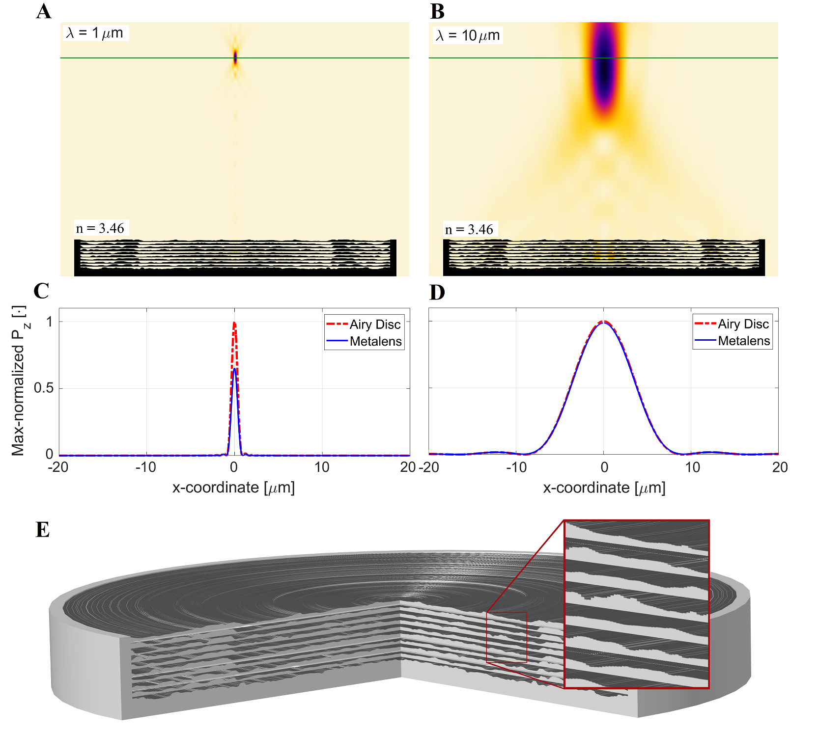
Figures 2A-2B show that the lens exhibits the desired numerical aperture at both wavelengths (green line). Further, the focusing capability of the lens is diffraction-limited for both wavelengths. The Strehl ratio (SR) at the two targeted wavelengths, m and m, is computed to SR and SR , respectively, from the data in Fig. 2C-2D.
Appendix D. Fabrication
The metalens was fabricated using a commercial two-photon polymerization system (Nanoscribe Photonic Professional GT) on a -micron-thick fused silica substrate, where the structures are written in circles with height increments of . For this purpose, piezo actuators move the sample in the out-of-plane direction after fabricating each layer. Geometrical parameters and dose (scanning speed and laser power) are optimized with a dose test on this specific machine. In the in-plane direction the laser beam is guided by galvanometric mirrors parallel to the substrate. After printing, the structures are put in a developer bath (PGMEA 5 min) and dried in IPA with a critical point dryer Auto Samdri 815 Series A.
Appendix E. Experiment
For the proof-of-concept experimental results presented in Fig. 4, we used the imaging setup shown in Fig. 6(a). A Ando AQ4321D Tunable Laser Source produces a fiber-coupled output at 1550 nm. The fiber output is collimated with a set of lenses. In the measuring configuration Fig. 6, the collimated beam is focused by the metasurface, and the focal spot is imaged by an objective - tube lens - IR imaging camera system. For this measurement, we used a 100X Mitutoyo Plan Apo NIR HR Infinity Corrected Objective, a ThorLabs mm tube lens, and a EC MicronViewer 7290A. The imaging setup was first calibrated using the configuration shown in Fig. 6(b), where the equivalent pixel size on the detector is evaluated by imaging a USAF1951 target. To evaluate the efficiency of the metasurface, we measured the equivalent power going through a m diameter pinhole with the configuration shown in Fig. 6(c).

To estimate the metasurface efficiency, we use the intensity-voltage relation of the NIR camera provided by the vendor. It has the form , where is the incident optical power on a pixel, the generated voltage at that pixel, and the characteristic nonlinear slope of the intensity-voltage relation, which is given to be . We first calibrate the proportionality constant by measuring the signal produced by the camera of a known beam power. This allows us to translate the measured voltage on a pixel to an incident power (in W). We also measure the incident intensity on the metasurface area with the experimental configuration shown in Fig. 6(c). The efficiency is then calculated as
where is the estimated optical loss through the objective and tube lens, which is 0.55 (objective) 0.88 (tube lens). We typically remove the background from the measured focal spot in order to estimate the metasurface efficiency.