Design of a -Ga2O3 Schottky Barrier Diode With p-type III-Nitride Guard Ring for Enhanced Breakdown
Abstract
This work presents the electrostatic analysis of a novel Ga2O3 vertical Schottky diode with three different guard ring configurations to reduce the peak electric field at the metal edges. Highly doped p-type GaN, p-type nonpolar AlGaN and polarization doped graded p-AlGaN is simulated and analyzed as the guard ring material, which forms a heterojunction with the Ga2O3 drift layer. Guard ring with non-polar graded p-AlGaN with band gap larger than Ga2O3 is found to show best performance in terms of screening the electric field at the metal edges. The proposed guard ring configuration is also compared with a reported Ga2O3 Schottky diode with no guard ring and a structure with high resistive Nitrogen doped guard ring. The optimized design is predicted to have breakdown voltage as high as 5.3 kV and a specific on resistance of 3.55 m-cm2 which leads to an excellent power figure of merit of 7.91 GW/cm2.
Index Terms:
Ga2O3, Schottky barrier diode, guard ring, GaN, AlGaN, Polarization doping, TCAD simulation.I Introduction
Gallium Oxide (Ga2O3) has a huge potential for power device applications due to its high breakdown field. -Ga2O3 has a band gap (4.6 eV) larger than GaN and SiC, with an estimated critical breakdown field as high as 8 MV/cm. Due to the large critical electric field, the Baliga Figure of Merit (BFOM) relevant to power switching could be 2000–3400 times that of Si, which is several times larger than that of SiC or GaN. Low doped drift layers in conjunction with large band gap materials can enable very high breakdown voltage. Various power devices using -Ga2O3 have been demonstrated recently with high breakdown voltage in the vertical geometry. [1, 2, 3, 4, 5, 6, 7, 8, 9, 10, 11, 12].
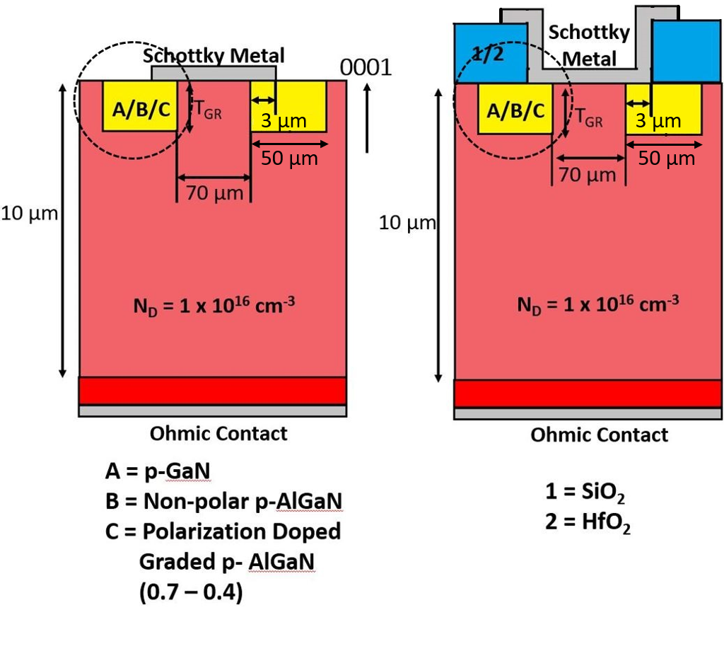
Several field management techniques have been explored for Schottky diodes over the years that includes edge terminations, superjunctions etc. Guard ring is one such edge termination technique where the anode metal edge is surrounded by a doped region with opposite polarity to that of the drift region to screen the high electric field generated at the metal edge. Lin et. al. [13] recently demonstrated a Schottky barrier diode (SBD) with nitrogen ion implanted guard ring (GR) with a maximum breakdown voltage of 1.43 kV. Zhou et. al. [14] also demonstrated a Ga2O3 SBD using Mg ion implanted guard ring with a breakdown voltage of 1.65 kV. A similar design with Argon implanted edge termination have also been reported by Gao et. al. [15]. Although these devices can achieve a breakdown improvement compared to the case with no guard rings, the lack of electric field screening due to the absence of carriers in the guard ring limits the breakdown voltage. A high resistive guard ring, as demonstrated in the previous devices can spread the depletion region and can reduce the field crowding at the metal edges. However, a guard ring with mobile holes can be very effective in screening the electric field at the metal edges due to the presence of a quasi neutral region and can dramatically shift the high field region from the metal edge to deep inside the device, thereby eliminating the effect of surface states which causes premature breakdown. Because of the difficulty in having hole concentration in -Ga2O3 due to the absence of a shallow acceptor and hole self trapping, p-doped III-Nitrides would be a viable option to get a reasonably high hole concentration. The idea of heterostructure guard rings have been proposed on Silicon Carbide substrate previously [16]. Muhammed et. al. [17] have reported the growth of c-plane n-GaN epilayer on ( 0 1) -Ga2O3 substrate using MOCVD. Vertical blue LEDs have also been demonstrated on ( 0 1) -Ga2O3 substrates [18]. Shimamura et. al. [19] reported growth of c-plane GaN on (1 0 0) oriented -Ga2O3 substrate using MOCVD. On the other hand Cao et. al. [20] reported the growth of non-polar a-plane GaN on (0 1 0) oriented -Ga2O3 substrate by MOCVD. All these reports confirm the viability of growing electronic grade polar and non-polar GaN on -Ga2O3 substrates depending on the choice of orientation of the substrate.
| Material | Ga2O3 | GaN | AlN |
|---|---|---|---|
| Bandgap (eV) | 4.85 [21] | 3.3 [22] | 6.2 [22] |
| Electron affinity (eV) | 3.9 [21] | 3.9 [22] | 0.6 [22] |
| Relative permittivity | 10 [21] | 8.9 [23] | 8.5 [23] |
| Electron Effective mass | 0.28m0 | 0.22m0 | 0.4m0 |
| Hole Effective mass | - | 1m0 | 4m0 |
| Critical Electric Field (MV/cm) | 8 [21] | 3.3 [23] | 15 [23] |
| Sn Activation energy (eV) | 0.13 [21] | - | - |
| Mg Activation energy (eV) | - | 0.2 [23] | 0.6 [23] |
| Spontaneous Polarization (C/m2) | - | -0.034 | -0.09 |


In this paper, we propose and design a Ga2O3 SBD with a p-doped III-Nitride guard ring using electric field simulations. We have explored three guard ring configurations including (i) p-Gallium Nitride (p-GaN) GR, (ii) Non-polar graded p-Aluminum Gallium Nitride (p-AlGaN) GR and a (ii) polar graded p-AlGaN GR. In this work we perform detailed electrostatic simulations to capture and manage high in III-nitride/-Ga2O3 heterostructures. The design is optimized to extract the optimum device parameters which efficiently reduces the electric field. We have also explored the additional use of field plate in the aforementioned optimum design to further minimize the peak electric field in the device structure.
II Simulation Methodology
The schottky barrier diode device structure (Fig. 1) with varied guard ring thickness of TGR, a 10 thick drift layer (ND = cm-3), Ni/Au Schottky metal with a barrier height of 1.4 eV [24], and a Schottky metal guard ring overlap of 3 m is simulated using Sentaurus [25] 2D TCAD device simulator. Width of the guard ring is considered to be 50 m. In the simulation, adequate numerical convergence was reached by an optimized meshing, with subnanometer grid spacing for the key electrical layers and their interfaces and larger spacings for drift region. Spontaneous polarization model is used to include polarization effect in the case of graded polar p-AlGaN.The sponataneous polarization values of -0.034 and -0.09 C/m2 is considered for GaN and AlN [23]. For p-type doping in GaN and AlGaN, incomplete ionization model is also used to reflect the accurate hole concentration. In order to capture the accurate results for high doping case, Fermi-Dirac model is included for device operating biases. The device simulation setup uses well calibrated mobility model and thermodynamic transport model to match the recent experimental results [13]. The device breakdown voltage can be extracted from E-field simulation when the peak E-field reaches the GaN (3.3 MV/cm) or Ga2O3 (8 MV/cm) critical E-field. Band offsets were determined using electron affinity rule. The GaN/Ga2O3 band offset estimated using electron affinity rule matches well with the experimentally determined band offsets [26]. The ionization integrals for avalanche breakdown were not evaluated in order to avoid excessive computation time. Furthermore, accurate ionization rate parameters are currently unknown for Ga2O3. Hence it should be noted that the breakdown is not directly calculated, but can be estimated based on the generated electric field distributions [27, 28, 29]. It should also be noted that in real devices field crowding can also occur in the device corners. However those fields are always lower than the field crowding at the electrode edges which is the primary cause of device breakdown. Hence our comparison of device breakdown for the various configurations based on 2-D simulation is considerably reliable and was also demonstrated by other works [27] .All the material parameters for - Ga2O3, GaN and AlN assumed in the device simulation are presented in Table I. All the other material parameters for intermediate Al compositions in AlxGa1-xN have been calculated based on GaN and AlN parameters using Vegard’s law.
III Results and Discussions
The SBD with nitrogen doped GR and the one with no GR is simulated for comparison and the electric field profiles are shown in Fig. 2(a) (i) and (ii) respectively. The circled cross-section in Fig. 1 is magnified and shown for all the electric field contours. The bias voltage is taken to be 1500 V. Ionization energy of Nitrogen in -Ga2O3 is considered to be 2 eV [30]. The maximum electric field is at the metal edge in both the cases and we can see that the field is reduced in the guard ring structure in Fig. 2(b) as expected and also experimentally reported [13].


We now explore the use of p-GaN as the guard ring material (Fig. 3(a)). The use a of magnesium-doped GaN guard ring, enables screening of the electric field at the metal edges due to the presence of mobile holes. The activation energy for Mg in case of p-GaN is considered to be 0.2 eV [31]. The doping concentration is taken to be (hole concentration = 8.2 1018 ) and the guard ring thickness is 0.5 and the anode voltage is 2000 V. The peak electric field has now moved to the p-GaN/n-Ga2O3 heterojunction as can be seen in the electric field contour shown in Fig. 3(a). Fig. 3(b) shows the equilibrium energy band diagram of p-GaN/n-Ga2O3 heterojunction. At the anode bias of 2000 V, the peak electric field at the p-GaN/n-Ga2O3 heterojunction exceeds the critical field of GaN (3.3 MV/cm). We simulated the p-GaN guard ring configuration as a function of anode voltage and the results are presented in Fig 5. The breakdown voltage of the p-GaN guard ring configuration presented here is 750 V.
To be able to leverage the high critical E-field of -Ga2O3, a better design would be to use a guard ring material with an enhanced critical field as compared to -Ga2O3 . So, we now study a graded p-AlGaN guard ring with aluminum composition graded from 70 at the AlGaN/Ga2O3 interface to 40 at the SBD surface. Lower Aluminum content is employed closer to the surface so as to achieve higher mobile hole concentration. Fig. 3(c) shows the electric field distribution using graded AlGaN for a doping concentration of . However since the ionization energy of Mg is very high for AlGaN with high Al composition, it is very difficult to realize a high hole concentration. In fact for Mg concentration below , the peak electric field is always at the metal edge because of the depletion of the entire GR. But if we grow c-axis oriented AlGaN with graded Al composition with decreasing Al composition from heterointerface to the surface, we can realize a 3-D slab of holes (3DHS) [32] due to the polarization doping effect. This is expected to significantly increase the hole concentration even with low Mg doping due to field ionization of dopants. Fig. 3(e) shows the electric field distribution in the polarization doped p-AlxGa(1-x)N (where x = 70 at the heterojunction to 40 at the SBD surface) GR. The hole concentration in this guard ring structure increased from the non-polar case by a significant amount (2 1017 to 6 1018 ). Band diagram of the polarization-doped polar graded p-AlGaN guard ring configuration is shown in Fig. 3(f). It can be observed that the peak electric field is now at the heterojunction mainly due to the positive polarization sheet charge at the p-Al0.7Ga0.3N/n-Ga2O3 heterojunction. The energy bands fall rapidly at the polar p-AlGaN/n-Ga2O3 interface, thus increasing the electric field compared to the non-polar p-AlGaN/n-Ga2O3 interface as shown in Fig. 3(g). Even for the low doped case, the bands fall rapidly at the p-AlGaN/n-Ga2O3 heterointerface as shown in Fig. 4. So, a polarization doped p-AlGaN GR would serve no benefit in reducing the peak electric field.


Fig. 5 shows the peak electric field vs applied bias for SBD with the five different guard ring structures. The doping concentration for p-type guard ring is taken to be of and for Nitrogen-doped case it is taken to be of and the GR thickness is taken to be 0.5 m. The non-polar graded p-AlGaN, ungraded p-AlGaN, and p-GaN guard ring shows best performance in terms of reducing the peak electric field. However the SBD with GaN guard ring crosses it’s critical electric field of 3.3 MV at 750 V. The non polar p-AlxGa1-xN GR with uniform Al composition (x = 60) has a critical electric field as high as gallium oxide and hence the breakdown voltage can be as high as 2000 V as shown in the Fig. 5. The electric field is very high in case of the SBD with polarization doped AlGaN GR because of the high field at the heterointerface.


Doping and thickness of the guard ring are critical parameters that would determine the amount of electric field screening and location of the peak electric field. We simulated the three guard ring configurations excluding the SBD with no GR and nitrogen-doped GR, as a function of Mg doping for a fixed thickness of 0.5 m at a bias of 2000 V. Doping in the guard ring is found to determine the location of the peak electric field as shown in Fig. 6. For the polar p-AlGaN guard ring, the peak electric field is always at the heterojunction irrespective of the doping. In the case of p-GaN and non-polar p-AlGaN guard ring, the peak field is at the metal edge for doping concentrations lower than . Since a high GR doping is not necessary to minimize the peak field at the metal edge and since non polar graded and ungraded p-AlGaN GR shows similar performance, compositional grading in the GR is not required, which will mitigate the challenge involving growth of graded epitaxial layer of AlGaN inside the pocket of Ga2O3.
The electric field simulations clearly establish the comparably superior performance of non-polar p-AlGaN guard ring configuration. We now further focus on this particular configuration and study the effect of thickness of the guard ring. In the case of low-doped guard rings, in order to take advantage of holes, it is essential that the the thickness must be sufficiently large to realize an undepleted region close to the metal. Equilibrium energy band diagram of non-polar graded p-AlGaN GR with low doping ( ) with two different thicknesses is shown in Fig. 7(a) and Fig. 7(b). Presence of a quasi neutral region near the metal by employing a thick low doped guard ring (Fig. 7(b)) is expected to be beneficial for electric field screening. The quasi neutral region near the metal edge provides room for the growth of the depletion region at high reverse bias. The effect of guard ring thickness as a function of Mg doping is summarized in Fig. 7(c). The peak electric field at a bias of 2000 V can be reduced from 9 MV/cm to 7.5 MV/cm at a guard ring doping of . The peak electric field reduces as the doping increases for doping concentration less than . As the GR thickness increases, the peak electric field reduces till a doping concentration of . Above this concentration the peak electric field shifts to the pn-heterojunction and the GR thickness has no effect on the peak electric field. In this regime, there is no advantage of using a field plate, since the peak field region is buried.

To further improve electric field management, we choose guard ring configuration B with a thickness of 1 m and doping concentration of 1016 cm-3. In this case, the peak electric field is at the metal edge. Now we analyze the potential for further improvement in breakdown voltage with a field plate. Fig. 8(a) shows the electric field distribution in the SBD for a GR thickness of 1 m and at a bias voltage of 3600 V (i) without and (ii) with a field plate respectively. An SiO2 layer of 200 nm is used as the field plate oxide. We also compared our design with a field plated SBD without GR as shown in 8(b). The field plating has more impact on the reduction of the peak electric field compared to the SBD with only GR. However, SBD having a field plate combined with a thick p-AlGaN GR dramatically reduces the peak electric field at the metal edge. Here again the peak electric field reduces as the doping increases till doping concentration reaches . So, the best design would be a thick low doped p-AlGaN GR with a field plate.
The Fig. 9 shows the effect of field plating on reducing the peak electric field for the SBD with non-polar p-AlGaN GR. In Fig. 9, we can see that for doping concentration less than , in the case of non-polar p-AlGaN GR, field plating significantly reduces the electric field at the metal edge and the electric field crosses the -Ga2O3 critical electric field of 8 MV/cm at a bias voltage of around 3600 V. For doping concentration above , the field plating has no effect on reducing the electric field because of shifting of the peak electric field from metal edge to the pn-heterojunction. We can also see that use of a high-k dielectric (HfO2, in this case with relative permittivity of 22) with same dimension as the previous case as field plate oxide in conjunction with the guard ring reduces the peak electric field dramatically and the device reaches the -Ga2O3 critical electric field of 8 MV/cm at a reverse bias voltage of 5200 V, which is significantly higher than the highest reported breakdown voltage for any vertical SBD with 10 drift layer [33]. The high permittivity difference between the semiconductor and the dielectric generates polarization bound charge inside the dielectric which balances the depletion charge at the semiconductor interface [29, 34, 35]. This charge balance results in flattening of the electric field profile at the dielectric/semiconductor interface reducing its peak magnitude. We have also simulated a field plated SBD with HfO2 as field plated oxide without a GR and it achieves a breakdown voltage of 4300 V. So, the use of a GR in conjunction with a field plate increases the breakdown voltage by 900 V compared to the field plated SBD with no GR. We have also analyzed other extreme high-k material such as BaTiO3 (relative permittivity of 300) as field plate oxide and the breakdown voltage was found to reach 7800 V when used in conjunction with GR. Since BaTiO3 has no conduction band offset with -Ga2O3, use of BaTiO3 underneath the metal might cause charge trapping at the dielectric/semiconductor interface. To mitigate the charge trapping, we have analyzed a stacked dielectric of HfO2 (5 nm)+BaTiO3 (295 nm). Here the large thickness ratio is used to maintain the high dielectric constant for the series configuration which results in an effective dielectric constant of 248. Using this structure in conjunction with the thick guard ring we are able to get a breakdown voltage of 6200 V.
Among all the devices described the SBD with non-polar p-AlGaN GR added with field plate and a high-k field plate oxide is found out to be best choice to reduce the electric field. The thick -Ga2O3 epilayers (10m) on (010) -Ga2O3 substrates used in this design can be grown using HVPE and has already been demonstrated [36, 37]. Selective area epitaxy of AlGaN GRs inside Ga2O3 trench pockets can be done using MOCVD [38, 39]. We understand AlGaN heteroepitaxy on Ga2O3 could lead to compromised material quality and will require extensive growth and process optimizations. Experimentally, trench Ga2O3 SBDs with field plate structures, were able to achieve FOM as high as 0.95 GW/cm2 [33]. Using the concepts explored in this work, if Ga2O3 SBDs with GR in conjunction with field plates are implemented, we expect this design to surpass the already high FOM achieved with Ga2O3 power SBDs. For instance, with a breakdown voltage of 6200 V and an estimated RON,SP of 3.55 m-cm2, assuming a mobility of 176 cm2/V.s [40], we should be able to achieve extremely high FOM of 10.8 GW/cm2.
IV Conclusion
A novel approach to reduce the electric field and thus increasing the breakdown voltage for schottky barrier diode by using p-doped III-nitride guard ring is proposed and shown through a detailed device simulation. This approach circumvents the issue of lack of p-type doping in gallium oxide. The SBD with thick low doped non-polar p-AlGaN GR in conjunction with a field plate and a high-k dielectric can serve best in terms of reducing the peak electric field. The inclusion of field plate and a high permittivity field plate oxide in case of low doped GR is shown to further reduce the electric field at the metal edges. Further research into the interface properties of the AlGaN/Ga2O3 heterointerface will lead to better understanding and use of such heterojunction-based structures for high performance power electronic devices.
Acknowledgement
This material is based upon work supported by the Air Force Office of Scientific Research under award number FA9550-18-1-0507 (Program Manager: Dr. Ali Sayir). Any opinions, finding, and conclusions or recommendations expressed in this material are those of the author(s) and do not necessarily reflect the views of the United States Air Force.
References
- [1] M. Higashiwaki, K. Sasaki, A. Kuramata, T. Masui, and S. Yamakoshi, “Gallium oxide (Ga2O3) metal-semiconductor field-effect transistors on single-crystal -Ga2O3 (010) substrates,” Applied Physics Letters, vol. 100, no. 1, p. 013504, 2012.
- [2] K. Sasaki, A. Kuramata, T. Masui, E. G. Villora, K. Shimamura, and S. Yamakoshi, “Device-quality -Ga2O3 epitaxial films fabricated by ozone molecular beam epitaxy,” Applied Physics Express, vol. 5, no. 3, p. 035502, 2012.
- [3] K. Sasaki, M. Higashiwaki, A. Kuramata, T. Masui, and S. Yamakoshi, “Ga2O3 Schottky Barrier Diodes Fabricated by Using Single-Crystal -Ga2O3 (010) Substrates,” IEEE electron device letters, vol. 34, no. 4, pp. 493–495, 2013.
- [4] M. Higashiwaki, K. Sasaki, K. Goto, K. Nomura, Q. T. Thieu, R. Togashi, H. Murakami, Y. Kumagai, B. Monemar, A. Koukitu et al., “Ga2O3 Schottky barrier diodes with n-Ga2O3 drift layers grown by HVPE,” in 2015 73rd Annual Device Research Conference (DRC). IEEE, 2015, pp. 29–30.
- [5] K. Konishi, K. Goto, H. Murakami, Y. Kumagai, A. Kuramata, S. Yamakoshi, and M. Higashiwaki, “1-kV vertical Ga2O3 field-plated Schottky barrier diodes,” Applied Physics Letters, vol. 110, no. 10, p. 103506, 2017.
- [6] J. Yang, S. Ahn, F. Ren, S. Pearton, S. Jang, J. Kim, and A. Kuramata, “High reverse breakdown voltage Schottky rectifiers without edge termination on Ga2O3,” Applied Physics Letters, vol. 110, no. 19, p. 192101, 2017.
- [7] K. Sasaki, D. Wakimoto, Q. T. Thieu, Y. Koishikawa, A. Kuramata, M. Higashiwaki, and S. Yamakoshi, “First demonstration of Ga2O3 trench MOS-type Schottky barrier diodes,” IEEE Electron Device Letters, vol. 38, no. 6, pp. 783–785, 2017.
- [8] J. Yang, S. Ahn, F. Ren, S. Pearton, S. Jang, and A. Kuramata, “High Breakdown Voltage (-201) -Ga2O3 Schottky Rectifiers,” IEEE Electron Device Letters, vol. 38, no. 7, pp. 906–909, 2017.
- [9] J. Yang, F. Ren, M. Tadjer, S. Pearton, and A. Kuramata, “2300 V reverse breakdown voltage Ga2O3 schottky rectifiers,” ECS Journal of Solid State Science and Technology, vol. 7, no. 5, p. Q92, 2018.
- [10] W. Li, Z. Hu, K. Nomoto, Z. Zhang, J.-Y. Hsu, Q. T. Thieu, K. Sasaki, A. Kuramata, D. Jena, and H. G. Xing, “1230 V -Ga2O3 trench Schottky barrier diodes with an ultra-low leakage current of 1 A/cm2,” Applied Physics Letters, vol. 113, no. 20, p. 202101, 2018.
- [11] W. Li, Z. Hu, K. Nomoto, R. Jinno, Z. Zhang, T. Q. Tu, K. Sasaki, A. Kuramata, D. Jena, and H. G. Xing, “2.44 kV Ga2O3 vertical trench Schottky barrier diodes with very low reverse leakage current,” in 2018 IEEE International Electron Devices Meeting (IEDM). IEEE, 2018, pp. 8–5.
- [12] Y. Wang, Y. Lv, S. Long, X. Zhou, X. Song, S. Liang, T. Han, X. Tan, Z. Feng, S. Cai et al., “High-Voltage (2 0 1) -Ga2O3 Vertical Schottky Barrier Diode With Thermally-Oxidized Termination,” IEEE Electron Device Letters, vol. 41, no. 1, pp. 131–134, 2019.
- [13] C.-H. Lin, Y. Yuda, M. H. Wong, M. Sato, N. Takekawa, K. Konishi, T. Watahiki, M. Yamamuka, H. Murakami, Y. Kumagai et al., “Vertical Ga2O3 Schottky barrier diodes with guard ring formed by nitrogen-Ion implantation,” IEEE Electron Device Letters, vol. 40, no. 9, pp. 1487–1490, 2019.
- [14] H. Zhou, Q. Yan, J. Zhang, Y. Lv, Z. Liu, Y. Zhang, K. Dang, P. Dong, Z. Feng, Q. Feng et al., “High-Performance Vertical Ga2O3 Schottky Barrier Diode With Implanted Edge Termination,” IEEE Electron Device Letters, vol. 40, no. 11, pp. 1788–1791, 2019.
- [15] Y. Gao, A. Li, Q. Feng, Z. Hu, Z. Feng, K. Zhang, X. Lu, C. Zhang, H. Zhou, W. Mu et al., “High-Voltage Ga2O3 Schottky Diode with Argon-Implanted Edge Termination,” Nanoscale research letters, vol. 14, no. 1, p. 8, 2019.
- [16] Q. Zhang, “Semiconductor devices with heterojunction barrier regions and methods of fabricating same,” Aug. 25 2015, US Patent 9,117,739.
- [17] M. Muhammed, M. Roldan, Y. Yamashita, S.-L. Sahonta, I. A. Ajia, K. Iizuka, A. Kuramata, C. Humphreys, and I. Roqan, “High-quality III-nitride films on conductive, transparent (-201) oriented Ga2O3 using a GaN buffer layer,” Scientific reports, vol. 6, p. 29747, 2016.
- [18] M. M. Muhammed, N. Alwadai, S. Lopatin, A. Kuramata, and I. S. Roqan, “High-Efficiency InGaN/GaN Quantum Well-Based Vertical Light-Emitting Diodes Fabricated on -Ga2O3 Substrate,” ACS applied materials & interfaces, vol. 9, no. 39, pp. 34 057–34 063, 2017.
- [19] K. Shimamura, E. G. Víllora, K. Domen, K. Yui, K. Aoki, and N. Ichinose, “Epitaxial growth of GaN on (1 0 0) -Ga2O3 substrates by metalorganic vapor phase epitaxy,” Japanese Journal of Applied Physics, vol. 44, no. 1L, p. L7, 2004.
- [20] Y. Cao, R. Li, A. J. Williams, R. Chu, A. L. Corrion, and R. Chang, “Non-polar GaN film growth on (0 1 0) gallium oxide substrate by metal organic chemical vapor deposition,” Journal of Materials Research, vol. 32, no. 9, pp. 1611–1617, 2017.
- [21] S. Pearton, J. Yang, P. H. Cary IV, F. Ren, J. Kim, M. J. Tadjer, and M. A. Mastro, “A review of Ga2O3 materials, processing, and devices,” Applied Physics Reviews, vol. 5, no. 1, p. 011301, 2018.
- [22] I. Vurgaftman, J. á. Meyer, and L. á. Ram-Mohan, “Band parameters for III-V compound semiconductors and their alloys,” Journal of applied physics, vol. 89, no. 11, pp. 5815–5875, 2001.
- [23] M. E. Levinshtein, S. L. Rumyantsev, and M. S. Shur, “Properties of advanced semiconductor materials : GaN, AlN, InN, BN, SiC, SiGe,” 2001.
- [24] A. Bhattacharyya, P. Ranga, M. Saleh, S. Roy, M. A. Scarpulla, K. G. Lynn, and S. Krishnamoorthy, “Schottky Barrier Height Engineering In -Ga2O3 Using SiO2 Interlayer Dielectric,” IEEE Journal of the Electron Devices Society, pp. 1–1, 2020.
- [25] Sentaurus Device User Manual, (Version N-2017.09, March 2017).
- [26] W. Wei, Z. Qin, S. Fan, Z. Li, K. Shi, Q. Zhu, and G. Zhang, “Valence band offset of Ga2O3/wurtzite GaN heterostructure measured by X-ray photoelectron spectroscopy,” Nanoscale research letters, vol. 7, no. 1, p. 562, 2012.
- [27] M. Xiao, R. Zhang, D. Dong, H. Wang, and Y. Zhang, “Design and Simulation of GaN Superjunction Transistors With 2-DEG Channels and Fin Channels,” IEEE Journal of Emerging and Selected Topics in Power Electronics, vol. 7, no. 3, pp. 1475–1484, Sep. 2019.
- [28] Y. Zhang, M. Sun, Z. Liu, D. Piedra, H.-S. Lee, F. Gao, T. Fujishima, and T. Palacios, “Electrothermal simulation and thermal performance study of GaN vertical and lateral power transistors,” IEEE Transactions on Electron Devices, vol. 60, no. 7, pp. 2224–2230, 2013.
- [29] Z. Xia, C. Wang, N. K. Kalarickal, S. Stemmer, and S. Rajan, “Design of Transistors Using High-Permittivity Materials,” IEEE Transactions on Electron Devices, vol. 66, no. 2, pp. 896–900, 2019.
- [30] M. J. Tadjer, J. L. Lyons, N. Nepal, J. A. Freitas, A. D. Koehler, and G. M. Foster, “Review—Theory and Characterization of Doping and Defects in -Ga2O3,” ECS Journal of Solid State Science and Technology, vol. 8, no. 7, pp. Q3187–Q3194, 2019.
- [31] M. A. Reshchikov, P. Ghimire, and D. O. Demchenko, “Magnesium acceptor in gallium nitride. I. Photoluminescence from Mg-doped GaN,” Phys. Rev. B, vol. 97, p. 205204, May 2018.
- [32] J. Simon, V. Protasenko, C. Lian, H. Xing, and D. Jena, “Polarization-induced hole doping in wide–band-gap uniaxial semiconductor heterostructures,” Science, vol. 327, no. 5961, pp. 60–64, 2010.
- [33] W. Li, K. Nomoto, Z. Hu, D. Jena, and H. G. Xing, “Field-Plated Ga2O3 Trench Schottky Barrier Diodes With a BV2/ R of up to 0.95 GW/cm2,” IEEE Electron Device Letters, vol. 41, no. 1, pp. 107–110, Jan 2020.
- [34] S. Rajan, Z. Xia, and C. Wang, “Dielectric passivation for electronic devices,” Jan. 2 2020, US Patent App. 16/455,736.
- [35] T. Kabemura, S. Ueda, Y. Kawada, and K. Horio, “Enhancement of Breakdown Voltage in AlGaN/GaN HEMTs: Field Plate Plus High- Passivation Layer and High Acceptor Density in Buffer Layer,” IEEE Transactions on Electron Devices, vol. 65, no. 9, pp. 3848–3854, 2018.
- [36] H. Murakami, K. Nomura, K. Goto, K. Sasaki, K. Kawara, Q. T. Thieu, R. Togashi, Y. Kumagai, M. Higashiwaki, A. Kuramata et al., “Homoepitaxial growth of -Ga2O3 layers by halide vapor phase epitaxy,” Applied Physics Express, vol. 8, no. 1, p. 015503, 2014.
- [37] J. Leach, K. Udwary, J. Rumsey, G. Dodson, H. Splawn, and K. Evans, “Halide vapor phase epitaxial growth of -Ga2O3 and -Ga2O3 films,” APL Materials, vol. 7, no. 2, p. 022504, 2019.
- [38] D. Kapolnek, S. Keller, R. Vetury, R. Underwood, P. Kozodoy, S. Den Baars, and U. Mishra, “Anisotropic epitaxial lateral growth in GaN selective area epitaxy,” Applied Physics Letters, vol. 71, no. 9, pp. 1204–1206, 1997.
- [39] Y. Kawaguchi, Y. Honda, H. Matsushima, M. Yamaguchi, K. Hiramatsu, and N. Sawaki, “Selective Area Growth of GaN on Si Substrate Using SiO2 Mask by Metalorganic Vapor Phase Epitaxy,” Japanese journal of applied physics, vol. 37, no. 8B, p. L966, 1998.
- [40] Y. Zhang, F. Alema, A. Mauze, O. S. Koksaldi, R. Miller, A. Osinsky, and J. S. Speck, “MOCVD grown epitaxial -Ga2O3 thin film with an electron mobility of 176 cm2/V s at room temperature,” APL Materials, vol. 7, no. 2, p. 022506, 2019.