Free-standing silicon nitride nanobeams with efficient fiber-chip interface for cavity QEDPreprint: AIP/123-QED
Abstract
We present the design, fabrication and characterization of high quality factor silicon nitride nanobeam PhC cavities at visible wavelengths for coupling to diamond color centers in a cavity QED system. We demonstrate devices with a quality factor of around the zero-phonon line of the germanium-vacancy center in diamond. We also present an efficient fiber-to-waveguide coupling platform for suspended nanophotonics. By gently changing the corresponding effective indices at the fiber-waveguide interface, we achieve an efficiency of at the cavity resonance.
The recent progress in quantum technologies has increased the demands for a robust scalable platform to realize an efficient quantum interface between light and matter. Building such interface is important for many applications ranging from optical sensing and metrology Simon, Jaeger, and Sergienko 2017 to quantum information and quantum computation Nielsen and Chuang 2002. One of the most promising type of platforms involves an atom coupled to optical resonator to allow a coherent energy exchange in a cavity QED system Cirac et al. 1997; Imamog et al. 1999; Chang et al. 2007. Towards this goal, several micro-cavities have been developed including Fabry-Perot cavities McKeever et al. 2004; Fortier et al. 2007, silica microspheres Vernooy et al. 1998, and microtoroids Armani et al. 2003. Despite the fact that aforementioned cavities possess ultra-high finesses and quality factors, their relatively large volume makes the integration of many devices in one chip very challenging. Instead, photonic crystal (PhC) cavities have recently emerged as a scalable platform for efficient light-matter interactions due to their small mode volumes accompanied with high quality factors Hennessy et al. 2007; Faraon et al. 2012; Sipahigil et al. 2016; Liu et al. 2015; Miura et al. 2014.
In this framework, Silicon nitride offers many advantages over other alternative materials, mostly due to its wide band gap and compatibility with standard CMOS processes. In visible wavelengths, however, the moderately low index of refraction has limited the quality factor of PhC cavities on Si3N4 films to only 3 orders of magnitude in visible wavelengths Trojak, Crane, and Sapienza 2018; Liu et al. 2017; Peyskens et al. 2019; Fryett et al. 2018; Barth et al. 2009. In this report, we demonstrate nanobeam PhC cavities with a quality factor of , that is 1 order of magnitude higher than previously reported.
On the other hand, nanobeam PhC cavities are not inherently suited to free-space optical coupling or fiber coupling due to the mismatch in the mode size and the effective refractive index. Previous work have used either notches Burek et al. 2014 or inverse-designed vertical couplers Dory et al. 2019 for free-space interfaces, and end-fire technique for fiber interfaces Cohen, Meenehan, and Painter 2013. The most efficient technique is based on evanescent coupling from a suspended waveguide to a biconical fiber taper Gröblacher et al. 2013 with an efficiency over 90. Here, we employ the same principle using a single-sided optical fiber tip and demonstrate a coupling efficiency of 96, similar to detached devices reported by Tiecke et al.Tiecke et al. 2015.


For the demonstration detailed here, we employed two designs (device A proposed by Ahn et al. 2010 and device B proposed by Ahn et al.Ahn et al. 2010 and from Alajlan et al.Alajlan, Cojocaru, and Akimov 2019) in which the nanobeam width is tapered smoothly while other parameters remain constant, as depicted in Fig. 1. We note that both devices are designed based on the quadratic tapering method which is meant to generate a Gaussian-like field profile inside the cavity Akahane et al. 2003; Quan and Loncar 2011. In both devices, we focused only on TE modes since the TM bandgap is absent. The corresponding band diagrams, displayed in Fig. 1 (b) and (c), show that adding semicircular holes in device B shifts the resonant frequency slightly towards the light line resulting in extra radiation loss. Nevertheless, this can be mitigated by increasing the width of the cavity or reducing the holes radii. The parameters have been adjusted such that the simulated intrinsic quality factor for both devices reaches . In practice, the spacing between holes needs to be adjusted to the point where the resonant frequency matches the target frequency. In our case, we adjusted the resonant frequency around nm, the zero-phonon line emission of the germanium-vacancy color center in diamond Iwasaki et al. 2015. The cavity transmission and quality factor dependence is shown in Fig. 1. It can be seen that the quality factor in device B exceeds the other one to some extent, similar to the case for gallium phosphide substrate Alajlan, Cojocaru, and Akimov 2019. The trade-off, however, is that device B is more sensitive to the fabrication imperfections which can be mitigated using a standard e-beam lithography (EBL) system explained next.
We carried out the fabrication on 200 nm thick stoichiometric Si3N4 membrane deposited via low-pressure chemical-vapor deposition on a plain Si substrate. Polymethyl methacrylate (PMMA) is first spun directly on top of the silicon nitride membrane without a metallic layer or conductive polymer Li et al. 2013. The resist is then patterned using an EBL system (TESCAN MIRA3) with an accelerating voltage of 30 kV, before developed in MIBK developer mixed with Isopropyl solution 1:3. Following the EBL process, the pattern is transferred to the Si3N4 using CHF3-based dry etching (ICP-RIE, Oxford Instruments). After stripping the resist, KOH solution is used to etch the exposed silicon at 100 °C for 10 minutes. SEM images of the final device is shown in Fig. 2.


For the quality factor measurement, a tunable laser was used and scanned around the TE fundamental mode, see Fig. 3. The experimentally measured quality factors for both devices are in the same order ranging from 10,000 to 24,000. Nevertheless, the dip transmission for device A is always larger as a result of the imperfection tolerance discussed above. It is worth noting that we have also fabricated devices on Si3N4 membrane deposited via plasma-enhanced chemical-vapor deposition and found that quality factors always are always one order magnitude lower than previously mentioned. This is mainly due to the higher hydrogen impurity density which leads to higher optical absorption Yota, Hander, and Saleh 2000. Nevertheless, the hydrogen impurity density can be decreased by annealing the nitride membrane at high temperatures Cai et al. 1996; Karunagaran et al. 2007.


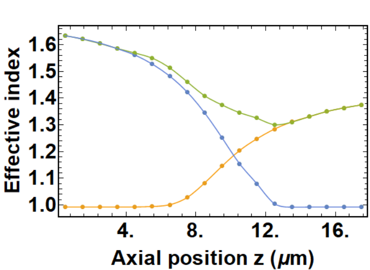
The light couples to the device using a single mode optical fiber tip that is coupled to the waveguide taper, see Fig. 4. This coupling technique is based on adiabatic transfer of an optical power between an optical fiber mode and a waveguide fundamental mode. The key idea is to change the effective refractive index of the target mode gently such that all the optical power are contained in the same mode profile. Therefore, the criterion of an adiabatic transfer is fulfilled if the change in the effective refractive index of the fundamental mode is less than the difference between effective refractive index of the fundamental mode and the nearest mode Gröblacher et al. 2013. This requires the tapering length to be longer than so-called beat length, the length over which the optical power could leak into a another mode. The beat length is given by Love et al. 1991, and it corresponds to 2 m for the geometry shown in Fig. 4. The waveguide is stretched over 10 m to ensure the stability of the optical fiber tip. In order to verify adiabatic mode transfer, FDTD simulations were performed in which a fundamental mode was launched at the beginning of the waveguide and monitored across the contact region, see Fig. 4. Simulation results shows that of the optical power has coupled to TE11 optical fiber mode, while the other leaks over the rectangular mechanical support that is connected to the chip. This result is in agreement to the side coupling approach aimed for detached devices Tiecke et al. 2015.


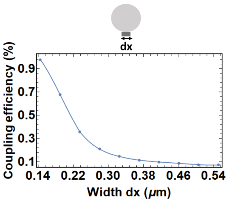
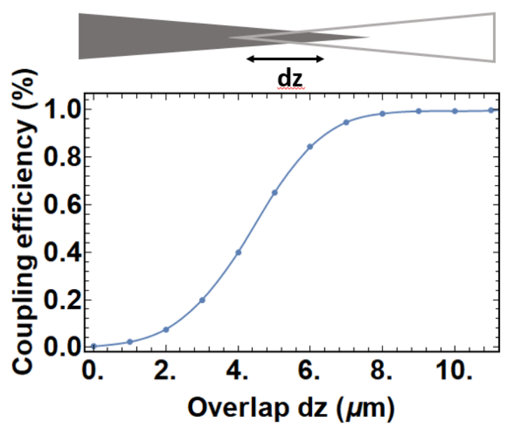
In order to characterize the influence of the rectangular mechanical support, we have calculated the coupling efficiency for various rectangle widths ranging from 1.4 m to 0.5 m. Figure 4 shows that the coupling efficiency drops exponentially as the rectangle width increases. This behavior is expected due to the swift change in the effective refractive index of the super-mode created in contact region. On the other hand, the length of the physical contact region in which an optical fiber tip overlaps with the waveguide taper is another crucial parameter. Figure 4 shows that the coupling efficiency saturates after the overlapping region reaches 7 m. This is relatively short compared to the biconical fiber taper technique previously reported Gröblacher et al. 2013.
The fabrication of an optical fiber tip is based on chemical wet etching approach in which a commercial single mode optical fiber (S405-XP, Thorlabs) is dunked in hydrofluoric acid (HF) covered by an organic solvent (e.g. xylene) to provide a oil-water interface 5. The non-stripped fiber is clamped on a motorized stage (MT1-Z8, Thorlabs) to control the pulling speed via a motor controller (KDC101, Thorlabs). The fiber diameter continues to shrink gradually as it is pulled out of the HF solution. The height of the oil-water interface mainly depends on the fiber diameter and the surface tension difference between the acid and the organic solvent Muramatsu et al. 1999. The key parameter in the fabrication process is the pulling speed that governs the angle of the optical fiber tip. The desired angle is dictated by the criterion of adiabatic transition of the fiber mode over the tapering region, similar to the waveguide taper discussed above. Since the cladding is etched away across the fiber tip, optical fiber cladding modes do not play any role in the coupling mechanism. This eases some restrictions in angles of the fiber tip which is limited to for an alternative technique that keeps the fiber cladding intact during the fabrication process Tiecke et al. 2015.
The fabricated optical fiber tips were characterized by several measurements. We first measure the power transmission of an optical fiber tip using a custom setup where an objective of 0.6 numerical aperture is used to collect the power from the end of the optical fiber tip. The collected power is then normalized to the power obtained from a similar optical fiber with a clean core/cladding cross section. We routinely obtain high power transmission () even for optical fiber tips with relatively large angles (). This measurement is necessary to ensure the adiabatic transition of the fiber mode all over the optical fiber tip. However, we sometimes observe low power transmission due to the fabrication imperfections such as insufficient acid etching and inaccurate fiber adjustment of the clamp, and some remains of polymer coating. These remains can be removed in piranha cleaning prior to the acid etching.


In the next measurement, we measure the coupling efficiency () between optical fibers and suspended Si3N4 cavities. The experiment is carried out as illustrated in Fig. 5. A supercontinuum laser (SuperK EVo, NKT Photonics) is launched into a dichroic mirror and then polarized before coupled into the fiber network where two photodetectors (PD1 and PD2) are used to record the ratio between the incoming and reflected optical power (). The optical fiber is placed on top of a 3-axis stage controlled precisely by a piezo controller (MDT693B, Thorlabs). Next, we connect a retroreflector device to the incoming beam instead of the optical fiber. The resulting ratio of obtained from two photodetectors () is used to calculate the coupling efficiency given by , where is the reflection of the cavity Bragg mirror which is assumed to be unity. For optical fibers with high power transmission, we routinely achieve a coupling efficiency . The maximum coupling efficiency we have achieved is . The error bar reflects the fluctuations in the data collected by photodetectors which is averaged over a long period. It is worth noting that the coupling between an optical fiber and device B is always lower than device A. The underlying reason is attributed to the back reflection at the mirror-waveguide interface Sauvan et al. 2005. Though we have appended transition holes to reduce the impedance mismatch in both devices, semicircular holes add more complexity at the transition region and require advanced tools for more precise adjustment. Nevertheless, we were able to achieved a coupling efficiency of for device B. In qualitatively analysis, we compare broadband reflection spectrum obtained from the cavity and that obtained from retroreflector device. Figure 5 shows that the ratio between the broadband reflection spectra approaches unity, confirming the efficient fiber-waveguide coupling discussed above.
In summary, we have presented the design, fabrication, and characterization of nanobeam PhC cavities based on silicon nitride at visible wavelengths. We were able to demonstrate devices with quality factors higher than by scanning laser around the cavity resonance. The device offers promising a platform for strong coupling in solid-state cavity QED experiments. Specifically, we aim to integrate diamond color centers with silicon nitride photonics platform to realize an efficient light-matter interface. In addition to diamond color centers, our device can be used for other single photon emitters such as quantum dots Park et al. 2015 and layered 2D materials Grosso et al. 2017. Moreover, we have developed a technique for coupling light from an optical fiber to on-chip suspended Si3N4 nanobeam PhC cavities. Utilizing the coupling technique presented here, we demonstrated a coupling efficiency of between an optical fiber mode and a cavity mode. This work is useful for quantum optics applications, including long-distance quantum networking Kimble 2008 and optical quantum computing O’brien 2007.
The authors would like to thank Denis Sukachev for valuable discussions. Financial support was provided by National Science Foundation (NSF) (PHY-1820930). Device fabrication is performed in part at the AggieFab Nanofabrication Facility at Texas A&M University. The authors acknowledge the Texas A&M University Brazos HPC cluster that contributed to the research reported here. The data that support the findings of this study is available from the corresponding author upon a reasonable request.
References
- Simon, Jaeger, and Sergienko (2017) D. S. Simon, G. Jaeger, and A. V. Sergienko, Quantum Metrology, Imaging, and Communication (Springer, 2017).
- Nielsen and Chuang (2002) M. A. Nielsen and I. Chuang, Quantum computation and quantum information (Cambridge University Press, 2002).
- Cirac et al. (1997) J. I. Cirac, P. Zoller, H. J. Kimble, and H. Mabuchi, “Quantum state transfer and entanglement distribution among distant nodes in a quantum network,” Physical Review Letters 78, 3221 (1997).
- Imamog et al. (1999) A. Imamog, D. D. Awschalom, G. Burkard, D. P. DiVincenzo, D. Loss, M. Sherwin, A. Small, et al., “Quantum information processing using quantum dot spins and cavity qed,” Physical review letters 83, 4204 (1999).
- Chang et al. (2007) D. E. Chang, A. S. Sørensen, E. A. Demler, and M. D. Lukin, “A single-photon transistor using nanoscale surface plasmons,” Nature physics 3, 807–812 (2007).
- McKeever et al. (2004) J. McKeever, A. Boca, A. Boozer, R. Miller, J. Buck, A. Kuzmich, and H. Kimble, “Deterministic generation of single photons from one atom trapped in a cavity,” Science 303, 1992–1994 (2004).
- Fortier et al. (2007) K. M. Fortier, S. Y. Kim, M. J. Gibbons, P. Ahmadi, and M. S. Chapman, “Deterministic loading of individual atoms to a high-finesse optical cavity,” Physical review letters 98, 233601 (2007).
- Vernooy et al. (1998) D. Vernooy, V. S. Ilchenko, H. Mabuchi, E. Streed, and H. Kimble, “High-q measurements of fused-silica microspheres in the near infrared,” Optics letters 23, 247–249 (1998).
- Armani et al. (2003) D. Armani, T. Kippenberg, S. Spillane, and K. Vahala, “Ultra-high-q toroid microcavity on a chip,” Nature 421, 925–928 (2003).
- Hennessy et al. (2007) K. Hennessy, A. Badolato, M. Winger, D. Gerace, M. Atatüre, S. Gulde, S. Fält, E. L. Hu, and A. Imamoğlu, “Quantum nature of a strongly coupled single quantum dot–cavity system,” Nature 445, 896–899 (2007).
- Faraon et al. (2012) A. Faraon, C. Santori, Z. Huang, V. M. Acosta, and R. G. Beausoleil, “Coupling of nitrogen-vacancy centers to photonic crystal cavities in monocrystalline diamond,” Physical review letters 109, 033604 (2012).
- Sipahigil et al. (2016) A. Sipahigil, R. E. Evans, D. D. Sukachev, M. J. Burek, J. Borregaard, M. K. Bhaskar, C. T. Nguyen, J. L. Pacheco, H. A. Atikian, C. Meuwly, et al., “An integrated diamond nanophotonics platform for quantum-optical networks,” Science 354, 847–850 (2016).
- Liu et al. (2015) X. Liu, T. Galfsky, Z. Sun, F. Xia, E.-c. Lin, Y.-H. Lee, S. Kéna-Cohen, and V. M. Menon, “Strong light–matter coupling in two-dimensional atomic crystals,” Nature Photonics 9, 30 (2015).
- Miura et al. (2014) R. Miura, S. Imamura, R. Ohta, A. Ishii, X. Liu, T. Shimada, S. Iwamoto, Y. Arakawa, and Y. Kato, “Ultralow mode-volume photonic crystal nanobeam cavities for high-efficiency coupling to individual carbon nanotube emitters,” Nature communications 5, 1–5 (2014).
- Trojak, Crane, and Sapienza (2018) O. J. Trojak, T. Crane, and L. Sapienza, “High-quality confinement of visible light in disordered photonic crystal waveguides in the anderson-localized regime,” (Optical Society of America, 2018).
- Liu et al. (2017) T. Liu, H. Qiu, T. Yin, C. Huang, G. Liang, B. Qiang, Y. Shen, H. Liang, Y. Zhang, H. Wang, et al., “Enhanced light-matter interaction in atomically thin mos 2 coupled with 1d photonic crystal nanocavity,” Optics express 25, 14691–14696 (2017).
- Peyskens et al. (2019) F. Peyskens, C. Chakraborty, M. Muneeb, D. Van Thourhout, and D. Englund, “Integration of single photon emitters in 2d layered materials with a silicon nitride photonic chip,” Nature communications 10, 1–7 (2019).
- Fryett et al. (2018) T. K. Fryett, Y. Chen, J. Whitehead, Z. M. Peycke, X. Xu, and A. Majumdar, “Encapsulated silicon nitride nanobeam cavity for hybrid nanophotonics,” ACS Photonics 5, 2176–2181 (2018).
- Barth et al. (2009) M. Barth, N. Nüsse, B. Löchel, and O. Benson, “Controlled coupling of a single-diamond nanocrystal to a photonic crystal cavity,” Optics letters 34, 1108–1110 (2009).
- Burek et al. (2014) M. J. Burek, Y. Chu, M. S. Liddy, P. Patel, J. Rochman, S. Meesala, W. Hong, Q. Quan, M. D. Lukin, and M. Lončar, “High quality-factor optical nanocavities in bulk single-crystal diamond,” Nature communications 5, 1–7 (2014).
- Dory et al. (2019) C. Dory, D. Vercruysse, K. Y. Yang, N. V. Sapra, A. E. Rugar, S. Sun, D. M. Lukin, A. Y. Piggott, J. L. Zhang, M. Radulaski, K. G. Lagoudakis, L. Su, and J. Vučković, “Inverse-designed diamond photonics,” Nature communications 10, 1–7 (2019).
- Cohen, Meenehan, and Painter (2013) J. D. Cohen, S. M. Meenehan, and O. Painter, “Optical coupling to nanoscale optomechanical cavities for near quantum-limited motion transduction,” Optics express 21, 11227–11236 (2013).
- Gröblacher et al. (2013) S. Gröblacher, J. T. Hill, A. H. Safavi-Naeini, J. Chan, and O. Painter, “Highly efficient coupling from an optical fiber to a nanoscale silicon optomechanical cavity,” Applied Physics Letters 103, 181104 (2013).
- Tiecke et al. (2015) T. Tiecke, K. Nayak, J. D. Thompson, T. Peyronel, N. P. de Leon, V. Vuletić, and M. Lukin, “Efficient fiber-optical interface for nanophotonic devices,” Optica 2, 70–75 (2015).
- Ahn et al. (2010) B.-H. Ahn, J.-H. Kang, M.-K. Kim, J.-H. Song, B. Min, K.-S. Kim, and Y.-H. Lee, “One-dimensional parabolic-beam photonic crystal laser,” Optics Express 18, 5654–5660 (2010).
- Alajlan, Cojocaru, and Akimov (2019) A. Alajlan, V. Cojocaru, and A. V. Akimov, “Compact design of a gallium phosphide nanobeam cavity for coupling to diamond germanium-vacancy centers,” Optical Materials Express 9, 1678–1688 (2019).
- Akahane et al. (2003) Y. Akahane, T. Asano, B.-S. Song, and S. Noda, “High-q photonic nanocavity in a two-dimensional photonic crystal,” Nature 425, 944–947 (2003).
- Quan and Loncar (2011) Q. Quan and M. Loncar, “Deterministic design of wavelength scale, ultra-high q photonic crystal nanobeam cavities,” Optics express 19, 18529–18542 (2011).
- Iwasaki et al. (2015) T. Iwasaki, F. Ishibashi, Y. Miyamoto, Y. Doi, S. Kobayashi, T. Miyazaki, K. Tahara, K. D. Jahnke, L. J. Rogers, B. Naydenov, et al., “Germanium-vacancy single color centers in diamond,” Scientific reports 5, 12882 (2015).
- Li et al. (2013) Q. Li, A. A. Eftekhar, M. Sodagar, Z. Xia, A. H. Atabaki, and A. Adibi, “Vertical integration of high-q silicon nitride microresonators into silicon-on-insulator platform,” Optics express 21, 18236–18248 (2013).
- Yota, Hander, and Saleh (2000) J. Yota, J. Hander, and A. Saleh, “A comparative study on inductively-coupled plasma high-density plasma, plasma-enhanced, and low pressure chemical vapor deposition silicon nitride films,” Journal of Vacuum Science & Technology A: Vacuum, Surfaces, and Films 18, 372–376 (2000).
- Cai et al. (1996) L. Cai, A. Rohatgi, D. Yang, and M. El-Sayed, “Effects of rapid thermal anneal on refractive index and hydrogen content of plasma-enhanced chemical vapor deposited silicon nitride films,” Journal of applied physics 80, 5384–5388 (1996).
- Karunagaran et al. (2007) B. Karunagaran, S. Chung, S. Velumani, and E.-K. Suh, “Effect of rapid thermal annealing on the properties of pecvd sinx thin films,” Materials Chemistry and Physics 106, 130–133 (2007).
- Love et al. (1991) J. Love, W. Henry, W. Stewart, R. Black, S. Lacroix, and F. Gonthier, “Tapered single-mode fibres and devices. part 1: Adiabaticity criteria,” IEE Proceedings J (Optoelectronics) 138, 343–354 (1991).
- Muramatsu et al. (1999) H. Muramatsu, K. Homma, N. Chiba, N. Yamamoto, and A. Egawa, “Dynamic etching method for fabricating a variety of tip shapes in the optical fibre probe of a scanning near-field optical microscope,” Journal of microscopy 194, 383–387 (1999).
- Sauvan et al. (2005) C. Sauvan, G. Lecamp, P. Lalanne, and J.-P. Hugonin, “Modal-reflectivity enhancement by geometry tuning in photonic crystal microcavities,” Optics Express 13, 245–255 (2005).
- Park et al. (2015) Y.-S. Park, S. Guo, N. S. Makarov, and V. I. Klimov, “Room temperature single-photon emission from individual perovskite quantum dots,” Acs Nano 9, 10386–10393 (2015).
- Grosso et al. (2017) G. Grosso, H. Moon, B. Lienhard, S. Ali, D. K. Efetov, M. M. Furchi, P. Jarillo-Herrero, M. J. Ford, I. Aharonovich, and D. Englund, “Tunable and high-purity room temperature single-photon emission from atomic defects in hexagonal boron nitride,” Nature communications 8, 1–8 (2017).
- Kimble (2008) H. J. Kimble, “The quantum internet,” Nature 453, 1023–1030 (2008).
- O’brien (2007) J. L. O’brien, “Optical quantum computing,” Science 318, 1567–1570 (2007).