Online Test Vector Insertion:
A Concurrent Built-In
Self-Testing (CBIST) Approach for Asynchronous Logic
Abstract
Complementing concurrent checking with online testing is crucial for preventing fault accumulation in fault-tolerant systems with long mission times. While implementing a non-intrusive online test is cumbersome in a synchronous environment, this task becomes even more challenging in asynchronous designs. The latter receive increasing attention, mainly due to their elastic timing behaviour; however the issues related with their testing remain a key obstacle for their wide adoption.
In this paper we present a novel approach for testing of asynchronous circuits that leverages the redundancy present in the conventional 4-phase protocol for implementing a fully transparent and fully concurrent test procedure. The key idea is to use the protocol’s unproductive NULL phase for processing test vectors, thus effectively interleaving the incoming 4-phase data stream with a test data stream in a 2-phase fashion. We present implementation templates for the fundamental building blocks required and give a proof-of-concept by an example application that also serves as a platform for evaluating the overheads of our solution which turn out to be moderate.
© 2014 IEEE. Personal use of this material is permitted. Permission from IEEE must be obtained for all other uses, in any current or future media, including reprinting/republishing this material for advertising or promotional purposes, creating new collective works, for resale or redistribution to servers or lists, or reuse of any copyrighted component of this work in other works.
I Introduction
Throughout the last decades we have witnessed a tremendous shrinking in the feature sizes of VLSI chips, paired with an increase of complexity. While, without doubt, these trends have been the key to the rapidly increasing performance, they also cause an increasing rate of faults per chip. In the face of extremely high transistor counts and small critical charges it is unrealistic to assume that a chip, once tested and put into operation, will perform its operation without further experiencing transient faults or permanent defects. Consequently, fault-tolerance provisions, e.g. based on concurrent checking or replication and masking, have been devised to cope with those faults and defects. However, all these approaches are based on assumptions about the multiplicity of faults – typically the single fault assumption – and they will fail when these are exceeded. While it is often sufficiently improbable that multiple faults coincide, the potential of fault accumulation is sometimes overlooked: A permanent fault that is tolerated within a fault-tolerance concept still uses up its fault-tolerance capacity, thus making the system vulnerable to the next fault that may occur, unless the first fault is properly removed. It is, e.g., well understood that a TMR architecture exhibits lower reliability than a simplex architecture, once one of the replica is affected by a permanent fault. This becomes particularly cumbersome for systems with long mission times. Therefore it is crucial, in addition to masking, to detect the existence of a fault, diagnose and remove it. The identification of faults may be non-trivial, especially when faults in rarely used resources must be considered that may remain undetected by concurrent checking approaches for a long time. This is where on-line testing becomes mandatory [1].
Asynchronous design is receiving increasing attention since it naturally avoids some of the most serious problems currently faced by synchronous designs, such as the need for low-skew clock distribution, insufficient tolerance to process, temperature and voltage (PVT) variations, and high power dissipation. Instead of a global clock it employs local handshaking to coordinate the activities, which makes operation demand driven and timing much more flexible. One of the main reasons why asynchronous design, although being around for several decades, has still not been widely adopted is the difficulty of testing – in the absence of a clock that the tester can use to control the test procedure, even their off-line test requires considerable efforts. In contrast, the approach we propose here naturally leverages the redundancy already present in the asynchronous 4-phase protocol for introducing test patterns into the data stream in a transparent fashion and fully concurrent with the ongoing operation. The key idea is to build components that present a conventional 4-phase interface to the outside, but internally operate with a 2-phase protocol, which allows test vectors to be inserted between any pair of regular data words, namely during the NULL phase of the external protocol. At the component’s output the results pertaining to the regular data stream are presented to the outside, again in a 4-phase fashion, while the test results are internally conveyed to a response analysis block.
The paper is structured as follows: After a review of related work we will present the fundamental concepts of the considered asynchronous design styles in Section III. Section IV will be devoted to presenting our approach in detail. A proof-of-concept implementation will be given and evaluated in Section V. Finally we will conclude the paper in Section VI.
II Requirements and Related Work
Concurrent checking is a well researched field in dependable computing. Its key principle is to employ some form of redundancy (hardware replication [2], coding [3], repeated execution of a calculation, etc.) to allow checking whether the result of a computation is correct. While this approach works fine for transient faults, it is not suitable for detecting permanent faults that may reside in a resource that is not exercised by the ongoing operation. Several of these dormant faults may accumulate over time and, once activated together, exceed the capabilities of the checking scheme. In order to safely unveil these faults one cannot simply rely on the ongoing operation to exercise the resources – a test is needed here that actively applies a well selected set of stimuli, independent of what is seen through normal system operation. This is another heavily researched area, however most approaches were developed for synchronous circuits, which sometimes leads to dissatisfying results when used on asynchronous ones.
We have argued above that actively applying test stimuli is desired and characteristic for testing. At the same time these stimuli deliberately change the state of the system under test, which interferes with the ongoing operation, and hence seems to make testing and regular operation mutually exclusive. Methods for online testing must fulfill two conditions: (value domain) non-interference with the system state perceived by the application and (time domain) no degradation of system performance beyond the point where deadlines are missed. This can be achieved by either interleaving phases of test and normal operation in a carefully controlled way, or by devising special test methods that remain transparent for the ongoing operation [4].
The key quality criteria of an online test are
- •
low performance penalty for the application
- •
high test coverage for a given fault model; this is determined by the quality and amount of test vectors
- •
low error detection latency; this is determined by the period required to apply the whole set of test vectors
We could not find approaches for a truly transparent test of asynchronous logic in the literature. The available methods either interrupt the ongoing operation [5] or simply check the output without actively applying test vectors [6]. An interesting combination of these two models is called input vector monitoring in [7]. Here a list of desired test vectors is determined as a subset of all possible inputs during operation. When one of these vectors is encountered during normal operation, the corresponding output is checked against a known reference, and the vector marked successful in the list. The test cycle completes as soon as all vectors in the list have been marked. Variations of this scheme have been proposed that differ in how strictly the sequence within the list must be kept; some even enter a dedicated test mode to apply vectors that are still missing after a timeout.
The approach we propose here is specifically designed for asynchronous logic. It provides a tight interleaving of test and ongoing operation and exploits specific protocol properties to largely eliminate performance penalties. It can be used with any arbitrary set of test vectors, whose generation can be carried out by standard methods from literature.
III Background
In synchronous systems all activities, specifically data exchange, are coordinated by a global clock. Asynchronous design, in contrast, employs explicit handshaking between communicating partners [8]: The sender indicates the validity of the data provided by means of a request (), while the receiver indicates their reception by means of an acknowledge () signal. This closed-loop principle is the root of the elastic timing behaviour of asynchronous designs. Depending on the specific interpretation associated with the transitions on and two protocols can be distinguished: In the 4-phase protocol (see fig. 1(a)) the sender indicates data validity by activating , to which the receiver responds by activating as soon as it has captured these data. This is followed by a return-to-zero phase, in which sender and receiver deactivate and , respectively. In the 2-phase protocol (see fig. 1(b)) that unproductive return-to-zero (RTZ) phase is avoided, and the falling transitions of and already guide the transfer of the next data item. This halves the number of control transitions per data transfer, which makes the 2-phase protocol the preferred choice when data needs to be transferred in an energy-efficient way. The 4-phase protocol, on the other hand, allows a more efficient implementation of logic functions and registers, and is hence usually employed for computation-centric blocks.
The indication of data validity via faces a fundamental race condition: The activation of must be perceived by the receiver only after data has actually become valid. The two principles used to ensure this pertain to different timing models of the circuit and have substantially different implementation complexity. In the bounded delay model a delay element is artificially inserted into the signal path that is chosen large enough to accommodate for all potential delays, including combinational functions, that the data may experience on its travel from sender to receiver. Obviously this necessitates a timing analysis and worst case assumptions, just like in the synchronous case. We will further refer to this approach as bundled data (BD), since it uses one for the complete bundle of data. In contrast, the delay insensitive11 1 For the sake of simplicity we disregard the notion of quasi-delay insensitivity here, for a more detailed discussion see e.g. [8] approach uses a more elaborate coding for the data that allows the receiver to evaluate, by means of a so-called completion detector, when a received data item is valid. In this way no explicit line is required any more, thus avoiding the race condition. The advantage of this solution is its ability to accommodate arbitrary delays on the data path without the need for worst case assumptions, its drawback is the necessity of data encoding (typically two signal rails per data bit are required). We will refer to this approach as completion detection (CD). In its 4-phase version two successive data items are separated by a so-called NULL spacer that establishes the RTZ phase. In the 2-phase version the coding itself allows a separation of successive data items.
Like in the synchronous case a fundamental structure for a data processing unit is a pipeline, in which register stages separate complex logic operations into smaller ones. The classical pattern in the asynchronous domain is the Muller pipeline shown in fig. 2. Its constituent component is the Muller C-Element, whose function is as follows: When both inputs match, the same value is reflected on the output; otherwise the output retains its last value. In the 4-phase operation that we will consider in the following, the latches in the datapath are transparent when is active, and opaque otherwise.
IV Proposed Approach
When comparing the data streams in fig. 1 one can realise that the 2-phase protocol works like a 4-phase protocol with extra data items being conveyed during the RTZ phase. In the CD case this can be understood as replacing the unproductive NULL spacer by productive data22 2 For the BD approach we assume early data validity [8], which is the most common approach anyway.. So when processing an incoming 4-phase data stream in a 2-phase function module, we obtain the freedom to insert a data items of our choice in place of the NULL spacers, (ideally) without loss of performance. The key idea of our approach is to use this freedom for inserting a stream of test data items into the original user data stream. Notice that, although we obtain an extremely tight interleaving between ongoing operation and test, this approach is completely decoupled from and transparent to the application, and allows choosing the test data freely.
Figure 3(a) illustrates the basic architecture of our proposed approach. At the input of the device under test (DUT) we place a 4-to-2 phase merge element (4-to2 PhM) that joins the 4-phase user data stream () with the 4-phase test data stream () into a single 2-phase data stream (). Of course, a source for the test vectors is required here, which is considered part of the self-testing module. In the following we will, however, not go into detail about which test vectors to actually select, these can be freely derived in accordance with the needs of the given DUT by means of the available test pattern generation techniques [9]. Here we will only be concerned with inserting a given test vector into the data stream and extracting the respective response later on.
The DUT now has to process the 2-phase data stream, so its design has to be converted from the original 4-phase protocol to 2-phase. This renders it more complex, which can somehow be considered the price for the online testing property. The DUT’s 2-phase output stream finally needs to be separated into the test responses and the results pertaining to the application input data, which are both again 4-phase. This task is performed by a 2-to-4 phase split element (2-to-4 PhS). The test responses can be analysed (compressed with a multiple-input shift register, e.g., and compared with a stored reference) inside the self-testing function block, while the application data stream is passed on to the actual output where it naturally appears as the 4-phase stream of results that one would expect in response to the original 4-phase input data stream. So from the outside the self-testing DUT behaves like a regular 4-phase logic block.
Interestingly, the approach allows an arbitrary choice of the DUT size: One extreme case would be to consider every single pipeline stage a separate DUT and equip it with all the required infrastructure at its input and output (fig. 3(b)). The other extreme would be to regard the complete design as the DUT(fig. 3(a)), thus trading controllability and observability for lower implementation overheads.
In the following we will focus on the description of the required merge and split elements, since they are fundamental for our approach, and we could not find suitable implementation patterns in the literature – only 2-phase/4-phase conversion of a single data stream [10] has been considered, or splitting and merging of datastreams following the same protocol [11, 12].
IV-A Merge and split for the bundled data approach
It is possible to compose the merge unit from two nearly independent blocks, one for handling the data bus and one for the control lines. The data handling block boils down to a multiplexer (MUX) that selects between forwarding the user data and the test data. In contrast to other approaches in the literature [11] we have a strict alternation between the two inputs and hence a fixed association between input source and state of in the 2-phase protocol on the output side. This allows to hardwire the MUX’s select input to the output , yielding low circuit complexity. In particular we chose to associate user data with and test data with . According to the bounded delay model an appropriate delay needs to be added before conveying the signal downstream, to compensate the data delay caused by the MUX.
For the output , termed in fig. 4, we want a rising edge when (a) the of the user data () rises, indicating new user data are available, and (b) the of the test data () falls, indicating the test vector generator is in its RTZ phase – whichever happens last. The same is true for the falling edge of , with the input transitions from and inverted. The Muller C-element shown in fig. 4(a) (top) serves exactly this purpose. The signal coming from the 2-phase function unit, termed can be simply conveyed as the to the user input (as ), and after inversion to the test input ().
For the 2-to-4 phase split element the data handling unit becomes trivial, namely just a set of wire forks: Since the data may assume any arbitrary value during the RTZ phase, all incoming data are directly forwarded to both outputs at the same time. It is up to the signals to indicate which of the outputs is intended to receive the respective data word. Recall that the merge unit associated user data with . Therefore we need to activate (and deactivate ) at the split unit output when the is seen at its input, and set (and deactivate ) otherwise. The simple circuit shown in fig. 4(b) (top) does this job and ensures that and are activated in a mutually exclusive fashion. Merging the responses and from the 4-phase outputs to a common 2-phase , namely , follows the same pattern as outlined for the signals in the merge unit. Not surprisingly, a Muller C-element with one inverted input, as shown in fig. 4(b) (bottom), does the job.
IV-B Merge and split for completion detection approach
From the available options for implementing the CD approach we chose NCL as the 4-phase protocol and LEDR as the 2-phase one. As these protocols use different data representations, a bit-level conversion becomes necessary in the merge and split unit. Table I shows the required mapping (per data bit). In the 2-phase protocol we have 2 rails per bit, one value rail () and one phase rail (). On the 4-phase side we have again 2 rails per bit, this time a one-hot code with one rail indicating high () and one low (). For the merge unit we need to convert from 4-phase to 2-phase (right-to-left in the table). Notice that in the 4-phase representation only a single rail is high at a time in each of the four valid states.
The circuit shown in fig. 5(a) identifies these states and maps them to the respective LEDR code. As the two 4-phase inputs (user data and test data) originate in different sources, we cannot avoid invalid intermediate input patterns (i.e. such with 2 rails or no rail at high). This is why we use Muller C-elements to retain the valid previous outputs during those phases. The can be treated in the same way as in the BD merge.
In the split unit the format has to be transformed back to the 4-phase protocol (left-to-right in Table I). Notice in the table how the alternation of test data and user data in the 2-phase stream leads to a natural insertion of the required NULL spacers into the 4-phase data streams. The required circuit can be easily derived and is not shown here. A purely combinational (glitch-free) implementation without Muller C-elements is sufficient here, since the 2-phase input does not exhibit invalid intermediate states.
Finally, the generation of the signal is again realised by connecting the incoming lines to a Muller-C element with the test in its negated form.
| 2-phase UTD | 4-phase UD | 4-phase TD | ||||||
| val | phs | int | hi | lo | int | hi | lo | int |
| 0 | 0 | LO(TD) | 0 | 0 | NULL | 0 | 1 | LO |
| 0 | 1 | LO(UD) | 0 | 1 | LO | 0 | 0 | NULL |
| 1 | 0 | HI(UD) | 1 | 0 | HI | 0 | 0 | NULL |
| 1 | 1 | HI(TD) | 0 | 0 | NULL | 1 | 0 | HI |
IV-C Enhancements
So far we have presented the basic implementations of the blocks handling the control signals. It is possible to increase their speed at the cost of increased complexity and thus increased area overhead. In the case of the merge element it is possible to acknowledge the NULL phase earlier, namely as soon as the data of the other input are propagated, giving the data values more time to travel through the logic. This yields advantages if NULL values are much faster than data values, which is the case when asymmetric delay lines are used. Another possibility is to propagate new data as soon as they show up, no matter if the other input has already delivered its NULL spacer or not, of course only after the was received from the succeeding stage. Furthermore, introducing a latch at the output of the merge unit makes it possible to acknowledge the inputs right away, resulting in a further decoupling of in- and output.
For the split unit it is possible, to start the NULL phase at the output that received the last data as soon as the input gets acknowledged. Another alternative is to acknowledge the input as soon as the output that recently received the data has acknowledged them, without the necessity of the other one having acknowledged its NULL phase. In addition a latch may be implemented at the input making it possible to acknowledge the input stream right away. For a more detailed and generic treatment of this topic see [13].
V Evaluation
We verified our online test approach for a three-stage Muller-pipeline. To keep the focus on the newly designed units, we did not introduce combinational functions between the pipeline registers; that would, however, be easy to add in a next step. More specifically we augmented the pipeline by a test vector generator, a response analyzer, and, most importantly, by our proposed merge and split units.
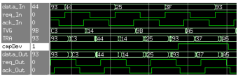
After synthesizing the VHDL design we carried out a post-layout simulation, whose result can be seen in fig. 6. The topmost three traces show the input signals to the DUT and the four traces at the bottom the output signals. represents the output of the test vector generator and the input of the test response analyser. The highlighted signal cmpDev gets high as soon as and mismatch, i.e. a fault is detected. Note how the values from and are processed in an alternating fashion and show up at the output with some delay corresponding to their propagation time through the pipeline.
To validate the self-testing capability of our approach we introduced a stuck-at-0 fault on bit 3 in our design. This fault is activated by the test vector which is transformed to (as well as the data vector being transformed to ). As soon as the TRA recognizes it raises cmpDev, as intended.
The area overhead and performance penalty introduced by our approach depend on many implementation parameters and are hard to estimate in general. We therefore decided to give an analytic estimation here that still allows to judge the influence of some choices, rather than presenting specific quantitative area and timing data from the synthesized design.
For the area overhead we compare the transistor count of the original pipeline with that of the enhancements required for the online testing feature. We do not include the TVG and the TRA in our analysis for two reasons: (1) The need for these units is common to all test approaches, and (2) depending on the specific demands the complexity of these units varies by orders of magnitude. In general, when mapping gates to transistor counts, we did not assume highly optimized cell designs, but we applied simplifications in the overall circuit when they were obvious (like reducing inverter count). The results of our analysis are shown in table II.
The first row analyses the bundled data case. In the first line the transistor count (unit “T” for “transistors”) for a stage (register plus control) of the original pipeline is given; in case the transistor count is proportional to the number of data bits “/DL” indicates “per data line”. Line 2 gives the overheads for the online test. The columns correspond to the individual function blocks (merge and split), with the rightmost column giving the overhead in depending on the number of stages, for large data width and without combinational logic. For the latches the overhead for conversion into a capture/pass latch according to [14] is accounted for as well33 3 In contrast to the implementation proposed in [14] we did not account T per switch but rather T (transmission gate).. In the BD approach the combinational function block (if any) remains unchanged. As there are substantially different ways of implementing the delay required in the BD approach, and furthermore the size largely varies with the required delay value, we did not include it here. This means that the initial size of the pipeline is underestimated here (making the relative overheads seemingly higher), and that the extra delay to compensate for the MUX introduction is not accounted for in the overheads.
The bottom row in table II shows the respective numbers for the CD approach. Here the conversion of the logic is far more complicated because each single gate has to be replaced. Unfortunately no concrete numbers could be found in the literature: That is why we make the pessimistic assumption that the transistor count will duplicate when moving from 4-phase to 2-phase44 4 In a very simple example that we used for a first comparison, we could build an XOR for NCL with about T, while its counterpart in LEDR required T, yielding an overhead of less than .. Furthermore, merge and split blocks need to be added, as well as the completion detector modified.
| merge | comb. | pipel. node | split | n stages (%) | ||
|---|---|---|---|---|---|---|
| BD | native | - | - | - | ||
| test | ||||||
| CD | native | - | - | - | ||
| test | * | |||||
As shown in Table II the overhead for the BD approach is . For a test-per-stage approach () this yields , while for a large number of pipeline stages between a single pair of merge/split elements, this value drops towards . With large logic function blocks this relative overhead, however, quickly approaches : Consider a combinational block of 12T/DL/pipeline stage; just this approximately halves the overhead.
For the CD approach with its more complex native pipeline stages the relative overhead is much lower. However, as, according to our pessimistic estimation, converting the logic function blocks roughly duplicates their transistor count, the situation does not improve with large function blocks.
For estimating the performance penalty we identify the additional delays introduced by the test infrastructure. To attain a generic view we consider gate delays (measured in inverter delays ID of the respective technology) and assume zero wire delays. The results are summarized in table III ( = number of data lines). They show the accumulated values for forward and backward () path. In all cases we assume that TVG and TRA operate fast enough to perform the handshaking without extra delays.
The numbers for the BD approach are shown in the first row, with the first line referring to the native implementation and the second one to the overhead for the online test infrastructure. The introduction of the merge and split units causes a delay of 5 and 2 ID, respectively. Relative to the stage delay this represents a penalty of more than . However, as the number of stages between merge and split, as well as the delays of the logic function blocks (not considered here) grow, the relative penalty quickly approaches . Similarly, the extra 1 ID for the register stage becomes negligible in case of complex combinational function blocks with high delays.
For the CD approach the picture is again initially better (penalty below ), as the native pipeline stage has more delay. The problematic point, however, is, once more, the complexity increase when transforming the combinational logic from 4-phase operation to 2-phase. The related performance penalty strongly depends on the specific circuit; we roughly estimate it as . Unfortunately, this number does not scale down with the number of stages or with the initial complexity of the combinational logic, as in the BD approach.
| merge | comb. | pipel. node | split | n stages (%) | ||
|---|---|---|---|---|---|---|
| BD | native | - | - | - | ||
| test | - | |||||
| CD | native | - | - | - | ||
| test | * | |||||
VI Conclusion
We have proposed to exploit the, normally unproductive, RTZ phase or NULL spacers of the asynchronous 4-phase protocols for conveying test vectors. While this can be done fully transparent and concurrent to the ongoing application, a new test vector can be applied after every single data word, which yields the tightest possible interleaving between test and operation, and hence an excellent detection latency. Test vectors can be freely chosen, independent from the user data, to optimize test coverage versus test period. We have identified the required infrastructure blocks for this approach and illustrated their basic implementation. In a case study we have proven the feasibility of the approach.
For the BD approach the area overheads can, according to our estimations, go up to under the most pessimistic assumptions. Fortunately they approach quickly with increasing number of stages and complexity of the combinational logic. The performance penalty can be close to , with the same favorable trends. So in practical cases the overheads will be very moderate. The CD approach exhibits lower relative overheads in the worst case scenarios, simply because the native implementation is more complex already. However, for the conversion of the combinational logic from 4-phase to 2-phase it is difficult to estimate the incident penalties. Under our pessimistic assumptions the overheads for this conversion dominate, and therefore we cannot attain the favorable scaling as seen with the BD approach.
However, even in the worst cases the observed overheads are still competitive with those of typical fault-tolerance methods like TMR, duplication or time redundancy, given the superior performance: In contrast to these fault-tolerance approaches that are based on concurrent checking, our online test detects permanent faults in the hardware, which are hard to unveil otherwise, with the best attainable (namely cycle-wise) interleaving between application and test.
Future work will be devoted to increasing the concurrency within the merge and split modules, as already sketched in this paper. This should aid in further reducing the performance penalty. Furthermore, it will be interesting to study the properties of the approach in more complex settings.
References
- [1] C. Scherrer and A. Steininger, “Dealing with dormant faults in an embedded fault-tolerant computer system,” IEEE Transactions on Reliability, vol. 52, no. 4, pp. 512–522, 2003.
- [2] T. Verdel and Y. Makris, “Duplication-based concurrent error detection in asynchronous circuits: Shortcomings and remedies,” in DFT. IEEE Computer Society, 2002, pp. 345–353.
- [3] R. W. Hamming, “Error Detecting and Error Correcting Codes,” The Bell System Technical Journal, vol. 29, no. 2, pp. 147–160, April 1950.
- [4] M. Nicolaidis and Y. Zorian, “On-line testing for vlsi - a compendium of approaches,” J. Electron. Test., vol. 12, no. 1-2, pp. 7–20, Feb. 1998. [Online]. Available: http://dx.doi.org/10.1023/A:1008244815697
- [5] D. Koppad and A. Efthymiou, “Bist for strongly-indicating asynchronous circuits,” in Very Large Scale Integration (VLSI-SoC), 2009 17th IFIP International Conference on, Oct 2009, pp. 215–218.
- [6] N. Minas, M. Marshall, G. Russell, and A. Yakovlev, “Fpga implementation of an asynchronous processor with both online and offline testing capabilities,” in Asynchronous Circuits and Systems, 2008. ASYNC ’08. 14th IEEE International Symposium on, April 2008, pp. 128–137.
- [7] K. K. Saluja, R. Sharma, and C. R. Kime, “A concurrent testing technique for digital circuits,” IEEE Trans. on CAD of Integrated Circuits and Systems, vol. 7, no. 12, pp. 1250–1260, 1988.
- [8] J. Sparso, S. B. Furber, Principles of Asynchronous Circuit Design: A Systems Perspective. Springer, 2001.
- [9] M. Bushnell, V. Agrawal, Essentials of Electronic Testing for Digital, Memory and Mixed-Signal VLSI Circuits. Springer, 2000.
- [10] A. Mitra, W. F. McLaughlin, and S. M. Nowick, “Efficient asynchronous protocol converters for two-phase delay-insensitive global communication,” in ASYNC, 2007, pp. 186–195.
- [11] M. Ferringer, “Conversion and interfacing techniques for asynchronous circuits,” in Design and Diagnostics of Electronic Circuits & Systems, 2011, pp. 11–16.
- [12] ——, “Conversion of two- to four-phase delay-insensitive asynchronous circuits,” in EUROCON. IEEE, 2011, pp. 1–4.
- [13] R. Najvirt, S. Naqvi, and A. Steininger, “Classifying virtual channel access control schemes for asynchronous nocs,” in Asynchronous Circuits and Systems (ASYNC), 2013 IEEE 19th International Symposium on, 2013, pp. 115–123.
- [14] I. E. Sutherland, “Micropipelines,” Commun. ACM, vol. 32, no. 6, pp. 720–738, Jun. 1989. [Online]. Available: http://doi.acm.org/10.1145/63526.63532