Analog electronics for beam instrumentation
Abstract
The task of analog front-end electronics in beam instrumentation is to optimize the useful information content of the signal delivered by an instrument. It must suppress signal components that do not contribute to the measured quantity. It must filter to put bounds on bandwidth and possibly dynamic range, to relax the demands made of subsequent processing stages. It must minimize noise, reject interference and match the signal to transmission media and digital acquisition equipment. Since the circuitry must often operate in radio-active areas, the accent is on passive electronics.
0.1 Introduction
It is tempting to just connect a measuring device to an ADC and to rely entirely on digital signal processing to extract useful information. Most often, this would be far from optimal. The signals produced by most transducers are a poor match to any ADC. To make the most of the available signal energy, analog signal conditioning is crucial. No amount of digital processing can recover information that isn’t there anymore. Analog electronics provide rejection of interference, filtering and amplification.
I can’t hope to give an anywhere near complete view of the vast subject of analog electronics. My purpose is rather to give you a taste of some useful subjects, with some hints, references and relevant keywords, so that you can look up more rigorous treatment elsewhere, should you need to do so. For a more comprehensive treatment of many subjects, the primary reference would be the excellent ’Art of Electronics’ [1]. Other useful references on electronics and instrument design are [3] and [2]. In this text, I chose to treat some subjects that I felt are somewhat neglected in most general treatises on electronics, but which are nevertheless significant for beam instrumentation.
Because beam instrumentation must often work in radio-active environments, where active semiconductor electronics may not survive for very long, much of what will follow concerns passive electronics.
0.2 Transmission lines
Transmission lines serve to carry signals from one place to another, of course, but are also used in transformers, splitters and combiners, hybrids and directional couplers, pulse forming networks, filters and resonators, bias and matching networks and more. A few of those applications, relevant to beam instrumentation, will be shown in what follows.

The most common transmission line is the coaxial cable (Fig. 1), a central wire completely enclosed in a conductive shield over its full length. The shield prevents the signal from radiating away and protects it from external fields. Such a cable is characterized by a distributed parallel capacitance and series inductance, determined by the geometry and by the materials used to make the cable. The capacitance, in farad/meter, can be found by applying Gauss’ law in the space between the conductors:
| (1) |
with the electric permittivity of the insulator in the space between the conductors. Similarly we can get the inductance in henry/meter using Ampère’s law:
| (2) |
with the magnetic permeability of the material inside. The resultant impedance seen by a signal source connected to an endless cable is then
| (3) |
is the characteristic impedance of the cable. Note that it’s a real value, a pure resistance. Commonly available coax can be had with impedances ranging from about 10 to 190 , but the most common values are 50 or 75 . For = 50 , typically = 100 pF/m and = 250 nH/m.
Practical cables also have a distributed series resistance and a parallel (leakage) conductance . Incorporating those into the expression for results in
| (4) |
which, unless , is now a complex value dependent on frequency. Often the leakage conductance is negligible, but the series resistance is not. These additional elements are responsible for transmission loss.
Although Eq. (4) doesn’t say so, the values of and are not constant. Both depend on frequency. is modified by the skin effect, the tendency of high-frequency AC currents to flow in a thin surface layer. is affected by dielectric losses. In a certain frequency range, generally from about 100 kHz to several gigahertz, the wire resistance and leakage conductance hardly affect the cable impedance which then converges on the value of Eq. (3). Cable loss expressed in decibels/m increases with the square root of frequency, which is pretty damning if you need to transport high-frequency signals over long distances.
0.2.1 Signal propagation
A signal in a coaxial transmission line can be thought of as an electromagnetic wave propagating through the space between the conductors. The wave is accompanied by co-moving charges in the conductors that compose the cable. The charge on the central conductor is mirrored by an opposite charge flowing along the inner surface of the screen. As a result, there are no magnetic or electric fields outside of the screen. This is the normal or odd mode of signal propagation. The signal propagation velocity in the cable is
| (5) |
In the absence of any dielectric material in the cable, this is equal to . Practical cables of course need some kind of insulating support for the central conductor, so and the signal propagation velocity is then reduced to , usually somewhere in the range of to , depending on the chosen dielectric and its consistency: solid, foam or discrete spacers. Usually, cables do not contain any magnetic materials, so .
It’s also possible to have a current flowing over the outside of the screen. This is the common or even mode. For that mode, the fields are in the space around the cable, with nothing inside. Whereas the odd mode has a well defined characteristic impedance , the even mode impedance is affected by the surroundings of the cable and is hard to predict. Even mode current is undesired and one seeks to reduce it as much as possible. This can be done, for example, by inserting transformers or baluns, sometimes simply by slipping a ferrite ring over the cable. More on this later.
0.2.2 Other forms of transmission lines
A transmission line doesn’t have to be coaxial. Whenever there is a convenient nearby conductor to support an image current, we have a transmission line. Commonly seen forms are twisted pairs, PCB tracks over full copper planes (stripline or microstrip), or parallel wires or PCB tracks (e.g. twin-lead, coplanar waveguide). For some geometries, a closed formula can give the characteristic impedance and for others, empirical approximated expressions exist. Many software tools exist to help, from very simple and free (e.g. atlc), to sophisticated EM field simulators (CST Microwave Studio, HFSS ,…).


0.2.3 Reflection and termination
Any discontinuity encountered by the propagating wave in a transmission line structure will cause a backward travelling reflection. The superposition of forward and backward travelling waves gives rise to standing waves, like vibrations in a taut string. However, if a finite length of transmission line is terminated with a resistance of value , no reflections will occur, since to the incident wave this just looks like the continuation of the transmission line.

It is possible to distinguish forward and backward travelling waves using directional couplers. A simple example of such a coupler is the Wheatstone bridge (Fig. 4). Assume all resistors are the same value. Consider a signal injected into port by source , with source zero. Since , no signal will appear across . Likewise, if we now inject a signal from source into port , with source zero, since , no signal will appear across . So across , we see only signal travelling right due to , and across , we see only signal travelling left due to . A circuit like this is at the heart of radio-frequency network analyzers.
A slightly different view, but which some reflection will show to be equivalent if and were coherent sinusoids, is the situation depicted in figure 6. Instead of an independent source with fixed source impedance , we substitute a variable impedance .


Any value of different from the other resistors will cause a reflection appearing across , in the same way as the backward travelling signal of figure 4.
| (6) |
The bilinear transformation Eq. (6), without the factor , is known as the reflection coefficient and it maps any passive complex impedance Z into a circle, with the perfect termination value in the centre. As is done in figure 6, we can draw new grid lines that allow us to read off the (normalized) value of Z directly from the value of . The grid lines are loci of constant real or imaginary parts of the impedance and are all circles. This is known as a Smith chart [4]. Before the generalized availability of computers, this chart was so useful as a graphical calculation aid that stylized pictures of the chart’s grid became trademarks for many companies involved in radio-frequency signal processing.
0.2.4 Time domain reflectometry
A very useful technique to sound the properties of transmission line structures, cables, connectors, vacuum feedthroughs and more is Time Domain Reflectometry (TDR). A fast step is launched into a transmission line structure, and the reflections, the echos, return information about what’s inside. The technique is eminently useful to locate faults in cables and connectors, yielding information about the location and the nature of the fault.


Figure 8 shows a simple example setup. A step signal is launched into a 1 m piece of coaxial cable. When the step hits the open end, a positive reflection with the same size as the incident step travels back towards the source. Figure 8 shows the measured response, taken with a 50-year old Tektronix sampling scope. The reflection gets back just before the 12 ns mark. The single-trip cable delay is just under 5 ns, half of the distance between the two steps. The T-junction connecting the transmission line to the oscilloscope must be compact.
Another example, figure 9, shows a piece of coax with a capacitor at its end. Initially, the step generator sees just a piece of coax. It has no way yet to know what’s at the far end. When the initial step reaches the end, from the viewpoint of the capacitor, this is just a step of twice the amplitude, applied from a source with impedance . The capacitor is charged according to
| (7) |
where is the open-source magnitude of the applied step voltage. This wave then travels back towards the generator to arrive there after another cable delay.

Side by side comparisons of measured and simulated data can profitably be used to build models of devices sounded by time-domain reflectometry, as illustrated in figure 11 and 11, showing the signals at the node marked ’tdr’ in figure 9.


A practical application of time-domain reflectometry for us beam instrumentalists is the optimization of a coaxial beam pick-up test bench. To test pick-ups or beam transformers in the lab, we string a rod or wire through the pick-up to which we apply test signals to simulate the passage of a beam. We can use TDR techniques to match the ends of the rod and to reduce any discontinuities. A smooth impedance guarantees a well-defined current through the pick-up.

Reflections would clutter the response, so it is good to carefully match both ends of the rod to minimize them. With the 30 ps risetime of the test instrument, it’s pretty hard to reduce reflections to below 3%. Precision geometry and RF-qualified components are needed to do this right.


Figure 14 shows a typical TDR trace of this setup. The vertical scale was normalized to the incident step which is off scale to the left of the plot. We recognize the residual discontinuities of the rod ends (at 0 and 11 ns), the impedance of the gap inside the Wall Current Monitor (at 5 ns) and we can identify the gaps between the vacuum flanges at each end of the WCM (at 4 and 8 ns). Figure 14 shows the response of one of the output ports of the WCM. The risetime is about 70 ps.
Note that a Fourier transform of differentiated time-domain reflection data will yield the frequency-domain reflection coefficient, from which the complex impedance can be found via Eq. 6). The reverse, applying an inverse Fourier transform to frequency-domain reflection data from an RF network analyzer, followed by integration over time will yield a TDR plot. Convolution in the frequency domain instead of integration/differentiation in the time domain will also work. Note that a TDR plot derived from frequency-domain data would show just the reflection, without the incident signal, because of the directional coupler in the network analyzer.
0.2.5 Transmission line transformers
Transmission line transformers are useful in analog signal processing as matching circuits to change voltage, current and impedance levels, as baluns and inverters, combiners, splitters, hybrids and directional couplers. The accessory fact that they are rad-hard is a useful feature for their use in beam instrumentation.
Ordinary transformers are bandwidth-limited by magnetic core losses, by leakage inductance and by parasitic capacitance. The useful frequency range can be extended considerably by arranging the windings to take advantage of transmission line coupling. In the context of RF transformers, it is customary to specify the impedance ratio rather than the turns ratio. The impedance ratio is simply the square of the turns ratio.
A basic example is the 1:4 Ruthroff transformer (Fig. 15, 17) [5]. The low-frequency equivalent circuit is just an autotransformer with a tap in the middle. The windings are laid down as a closely-spaced pair of wires. This ensures that transmission line coupling takes over at frequencies where magnetic coupling through the flux in the core fails, thus extending the useful bandwidth. About three decades of bandwidth are achievable.


These transformers have a null in the frequency response where the wavelength in the transmission line formed by the wire pair is , because the delayed signal from the output end of the transformer is fed back into the input. This implies that the wires must be kept as short as possible to preserve the high frequency performance.
Figure 17 (red curve) shows the measured frequency response of the transformer in figure 15, left. On the input side, a source drives the circuit. The transformer increases the the voltage at its input port by a factor of two, +6 dB. On the output side, the load must be , composed here of a resistor in series with the input resistance of the measurement instrument, an RF Network Analyzer. This forms a resistive divider of 1/4, or -12 dB. Thus the level of the flat portion of the response as seen by the instrument is -6 dB.


The lower cut-off frequency is where the inductive reactance of the winding drops below . The upper cut-off frequency occurs where the length of the winding reaches and there is a null at twice that frequency. The transformer incurs a little loss, usually well below 1 dB in the flat portion of the response. The green curve is the reflection coefficient in decibels, a measure of how closely the transformer’s input impedance matches 50 . (See also Eq. (6)).
It is possible to obtain other transformation ratios by adding or removing one or two turns from one of the windings, or by using three or more wires instead of just two. Even though this stretches the concept of a transmission line a bit, results are often quite acceptable [6].
It is also possible to use coax cable for the windings (Fig. 18). The centre conductor replaces one wire and the screen conductor replaces the other. It may be more practical to thread the coax straight through multiple cores rather than to try to wind it on a single core.


The coax impedance should ideally be the geometrical mean of input and output impedances. It is advisable to select the screen for the conductor with the smallest signal potential, to minimize the effects of parasitic capacitances. The advantage of coax is the possibility to obtain lower leakage inductance, allowing higher frequency operation. Otherwise, the same reasoning as for the wire-wound transformers applies.
The interesting thing about transmission line transformers is that their performance at high frequencies depends but little on the properties of the magnetic cores. The cores serve only to impede common-mode current. The core and windings are dimensioned so that the common-mode inductive reactance at the lower end of the design bandwidth is greater than the combined port impedances. In addition, the core size should be such that it does not saturate at the rated power level and the lowest frequency. The usual core choices are toroids of high-permeability ferrite, or amorphous or nano-crystalline magnetic alloys.
Balun transformers
The word balun is a contraction of balanced-to-unbalanced. The general topology is a transformer turned on its side (Fig. 19). Both windings are wound together on a single core, in a similar way as in figure 17. The idea is that the left and right sides of the transformer are separated by the common-mode inductance of the windings, lending almost complete freedom in choosing the grounding points on either side. This works for frequencies where the common-mode impedance becomes greater than the source and load impedances.


In the examples shown in figure 19, the input source is always single-ended and referenced to ground, but this is entirely optional. The top left diagram is the trivial case, with the bottom side of the load resistance R also connected to ground. The load sees an untransformed signal, albeit delayed by the length of the transmission line. At the bottom left, the load resistance is grounded at the other end. The balun now acts as an inverter. In the top right diagram, the centre of the load resistance is connected to ground. The load now gets driven symmetrically. This is the application from which this class of transformers derives its name. A minor issue is that there is still some current flowing through the common mode impedance of the transformer, which also flows through the top half of the load, but not through the bottom half. As a result, the symmetry is a little off, worse at low frequencies. The extra winding in the bottom right diagram fixes that by providing an alternative path for that current.
Again, the necessary common-mode inductance may be obtained by winding the conductors on a high-permeability toroid cores. Here too, the high-frequency properties of the cores hardly matter. Even though core losses cause the common mode impedance to become resistive –rather than inductive– above a few megahertz, it will usually remain comfortably higher than the winding’s differential mode impedance, which is sufficient (Fig. 21).


Again, coax cable can be used instead of wire. A simple example implements the inverting transformer of figure 19, bottom left: Cross the shield and core conductors near the middle of an ordinary piece of coax 60 cm long and you’d have an excellent inverting transformer (Fig. 21). A 60 cm length of coax –any electronics lab has lots of those– has a common mode inductance of about half a microhenry, the impedance of which exceeds the characteristic impedance of the coax above about 8 MHz. So the useful frequency range starts at 8 MHz and reaches up to over 6 GHz (Fig. 23, red curve).


But it gets better: By slipping a handful of ferrite cores over the cable, it’s easy to raise the common mode inductance to several tens of microhenries. The transformer then also works at much lower frequencies, like the green curve in figure 23. With little effort, we have made an inverting transformer with a bandwidth of 100 kHz to over 6 GHz. Pretty impressive for such a simple thing! Since above 8 Mhz the EM fields are entirely confined inside the coax, the ferrite properties are largely irrelevant there. The core has to ’work’ only from about 100 kHz to 8 MHz.
Equal delay transformers
Baluns can be combined to create equal delay or Guanella transformers [7]. Here, the idea is to effect impedance transformations by connecting transmission line baluns in series(parallel) on one side, and in parallel(series) on the other. If the transmission lines have equal lengths, signals add in phase at the output and the frequency response is flat. Figure 25 shows such a transformer with a 1:4 ratio. The high-end frequency is limited only by the inevitable inductance of the interconnections, by the capacitance to the upper transmission line, which has an RF voltage on its screen, and by length mismatches between the lines.


Implemented with coax, it would have a impedance at the left side and a impedance at the right. It is not unreasonable to expect the bandwidth to stretch from a few tens of kiloherz up to several gigaherz.
The impedance ratio of Guanella transformers is not limited to only the squares of the integers. In principle, any rational transformation ratio can be obtained by various combinations of parallel and series connections of transmission lines, see, for example, figure 25. (The necessary ferrite cores for the top two lines are not shown. The bottom line needs none because there is no common mode voltage across the ends.) Many combinations are detailed in [8]. In practice the range is limited by parasitic inductances and capacitances, and by the difficulty of joining many transmission lines in a compact way.
Combiners, splitters and hybrids
Another class of transmission line transformers combines the signals from two independent sources together on a single output, while preventing any power flow between the inputs.


Figure 27 shows a wire-wound version. The two input signals are added together and appear at the output at half the original source impedance. Resistor is necessary to provide isolation between the inputs and absorbs the difference between the inputs. Its value is twice the original source impedance, because it sees the inputs in series, whereas the sum output sees the inputs in parallel instead. Figure 27 shows a possible implementation of the same thing using coaxial cable. Using either transformer in reverse, exchanging inputs and outputs, they would operate as splitters.


A minor change turns the circuit of figure 27 into a 180∘ combiner, subtracting the inputs rather than adding them (Fig 29). Instead of dumping the difference into a resistor, we use a balun to transform this balanced signal to a single-ended output. We now dump the sum signal into a resistor.
Figure 29 shows a different way to extract a single-ended difference. In addition, this transformer also puts out the sum at the same time, so it’s now a hybrid. The three wires are wound on a single core. If the number of turns is the same for all three windings, the difference signal will also have an impedance of , like the sum. Such hybrids are often used in beam position monitor signal processing.
Combining several of the transformers described above, it’s possible to construct hybrids with impressive bandwidths. Figure 30 shows the simplified schematic of a hybrid covering a bandwidth from 6 kHz to 600 MHz. It uses a Ruthroff-type transformer for the sum output and a cascade of a Guanella balun and a three-wire balun to construct the difference output.

Figure 32 shows the practical construction, using thin coaxial cable and one piece of wire. This hybrid is used for several wide-band beam position monitors in CERN’s PS complex [9]. Figure 32 shows the measured frequency response of the hybrid. For this application, the useful bandwidth is limited at the high end, not so much by signal drop-off, as by the leakage of the sum signal into the difference output.


0.3 Filters
Passive LC filters are indispensable between a transducer and the first stage of active electronics. They protect against out-of-band signals and reduce the bandwidth and dynamic range demanded of amplifiers and ADCs. They improve the signal to noise ratio by rejecting out-of-band noise. Passive filters are also used as reconstruction filters after a DAC, PWM or class-D output stage.
Many passive filters were developed and categorized on some useful properties in the 1940’s. Pre-computed tables of normalized element values exist for filters that are optimized for clean impulse response or steep frequency response, with variants trading some parameters against others [10]. Trade-offs can be made against properties such as steepness, passband ripple, ultimate attenuation, phase linearity and complexity. The calculation of element values ab initio is beyond the scope of this text [11].
Passive filters are designed to provide the intended response with a specified source and load impedance. It’s important to realize that stop band energy is reflected back to the source, which must be able to absorb it. We shall see a few examples of filter designs based on tables of normalized element values. Many commercial software tools exist to assist with filter design.
If the application requires good pulse shape fidelity, we use filters that approximate linear-phase behaviour –constant group delay–, such as the Gaussian, Bessel or equi-ripple phase error filters. Such filters have gently sloping frequency responses. If the application calls for a steep drop-off, Chebyshev or Cauer filters might be chosen, but the phase response will be poor and the impulse response will ring. The Butterworth filter is in between, falling off faster than the Bessel but having better impulse response than a Chebyshev. See the curves in figures 34 and 34.


We use the tabulated values for a normalized low-pass ladder filter as a starting point. (Table 1, figure 35). The filter may start with a series inductor or a shunt capacitor, and other circuit considerations must decide which is most appropriate.

| C1 | L2 | C3 | L4 | C5 | L6 | C7 | |
|---|---|---|---|---|---|---|---|
| L1 | C2 | L3 | C4 | L5 | C6 | L7 | |
| 2 | 0.5755 | 2.1478 | |||||
| 3 | 0.3374 | 0.9705 | 2.2034 | ||||
| 4 | 0.2334 | 0.6725 | 1.0815 | 2.2404 | |||
| 5 | 0.1743 | 0.5072 | 0.8040 | 1.1110 | 2.2582 | ||
| 6 | 0.1365 | 0.4002 | 0.6392 | 0.8538 | 1.1126 | 2.2645 | |
| 7 | 0.1106 | 0.3259 | 0.5249 | 0.7020 | 0.8690 | 1.1052 | 2.2659 |
The element values in table 1 are normalized to unit load resistance and unit cut-off angular frequency. They are to be scaled to the required impedance and frequency. The relations between the normalized and the real values for target cut-off angular frequency and load impedance are
| (8) |
As an example, let’s make an O(6) Bessel filter with a 20 MHz cut-off frequency for source and load impedances. The angular frequency , so we find and . Figure 36 shows both the normalized and the scaled element values for this filter and figure 37 shows its frequency response. Note that the curve goes through -3 dB, its half power point, at 20 MHz, just as intended.


Zverev lists extensive tables of element values for different filter types and a selection of source resistances [10]. These cover the great majority of filtering applications.
0.3.1 Constant input impedance filters
Constant input resistance filters do not reflect unwanted energy. This is useful, for example, if the filter is required to terminate a long cable, or if the source won’t absorb reflected energy. This is often the case in beam instrumentation. An additional feature of such filters is that the shape of the frequency response is independent of the source resistance. These properties make constant input resistance filters very useful in many applications.
The starting point for the design of a filter with constant input resistance is the normalized lowpass prototype for zero source impedance. This is the filter that produces the desired response with a constant input level as a function of frequency.
All such filters start with a large series inductance. Therefore, the input impedance as a function of frequency will tend to rise above cut-off. A shunt impedance across the filter input must be added to maintain constant input resistance. For Butterworth filters this is easy (Table 2). It’s sufficient to add the dual circuit, like the example for an O(5) filter, in the dashed box in figure 38. It has inductors where the normal filter has capacitors and vice-versa, and the component values are the reciprocals of the values in the normal filter.
| L1 | C2 | L3 | C4 | L5 | |
| 5 | 1.5451 | 1.6944 | 1.3820 | 0.8944 | 0.3090 |

| L1 | C2 | L3 | C4 | L5 | C6 | L7 | |
|---|---|---|---|---|---|---|---|
| 3 | 1.4631 | 0.8427 | 0.2926 | ||||
| 4 | 1.5012 | 0.9781 | 0.6127 | 0.2114 | |||
| 5 | 1.5125 | 1.0232 | 0.7531 | 0.4729 | 0.1618 | ||
| 6 | 1.5124 | 1.0329 | 0.8125 | 0.6072 | 0.3785 | 0.1287 | |
| 7 | 1.5087 | 1.0293 | 0.8345 | 0.6752 | 0.5031 | 0.3113 | 0.1054 |
For other filters, this simple recipe doesn’t work, but it is sometimes still possible to derive the perfect matching impedance.

For example, consider the O(5) Bessel filter of figure 39. This filter’s input impedance is
| (9) |
where . To obtain a constant input resistance, we would have to add a matching shunt impedance across the input such that
| (10) |
Solving for , we find
| (11) |
This can then be expanded into a continued fraction from which we can read the component values of a ladder circuit implementing the required shunt impedance
| (12) |
A symbolic math program removes most of the tedium of working this out. So the final (still normalized) constant-impedance filter ends up as shown in figure 40. Matching network values for several more Bessel filters are listed in table 4. Element Z2 is omitted from the table. Its value is always unity.

| Z1 | Z3 | Z4 | Z5 | Z6 | Z7 | Z8 | |
|---|---|---|---|---|---|---|---|
| 3 | 0.913F | 1.755+2.428H | 2.428F | ||||
| 4 | 0.925F | 1.570+2.407H | 2.413//0.5469F | 3.240+1.447H | |||
| 5 | 0.931F | 1.568+2.424H | 3.522//0.5240F | 1.513+1.589H | 1.111//0.303F | ||
| 6 | 0.935F | 1.616+2.446H | 4.276//0.5012F | 1.009+1.679H | 2.514//0.330F | 3.558+0.945H | |
| 7 | 0.936F | 1.669+2.465H | 4.647//0.4838F | 0.777+1.709H | 4.004//0.347F | 1.656+1.110H | 1.131//0.191F |
Although this works for Bessel filters of any order, for orders greater than three, there is a simpler solution which works just as well in practice. A series RC circuit across the filter input can restore the input impedance to unity for very high frequencies, and a series RLC resonator can be positioned over the transition region to minimize the impedance bump (Fig. 41, box).

| Ca | Cb | Lb | Rb | L1 | C2 | L3 | C4 | L5 | C6 | L7 | |
|---|---|---|---|---|---|---|---|---|---|---|---|
| 3 | 0.5804 | 0.3412 | 0.9915 | 2.6161 | 1.4631 | 0.8427 | 0.2926 | ||||
| 4 | 0.6121 | 0.3143 | 1.0646 | 2.7036 | 1.5012 | 0.9781 | 0.6127 | 0.2114 | |||
| 5 | 0.6465 | 0.2834 | 1.1613 | 2.8896 | 1.5125 | 1.0232 | 0.7531 | 0.4729 | 0.1618 | ||
| 6 | 0.6622 | 0.2683 | 1.2094 | 3.0029 | 1.5124 | 1.0329 | 0.8125 | 0.6072 | 0.3785 | 0.1287 | |
| 7 | 0.6876 | 0.2452 | 1.2955 | 3.2070 | 1.5087 | 1.0293 | 0.8345 | 0.6752 | 0.5031 | 0.3113 | 0.1054 |
As can be seen in figure 42, the calculated reflection coefficient is nearly everywhere below dB, meaning that never strays by more than about 0.3% from unity. Although this is not perfect, it is still much better than what can actually be achieved with realistic component tolerances.

Table 5 lists the element values for some Bessel filters with the associated matching circuits. Moreover, this can be done for some other filter types too. Element values for Bessel filters up to O(10), as well as for Gaussian and some equi-ripple phase error filters are given in [12].
To summarize, the exact matching network obtained by solving Eq. (10) is fine for low order Bessel filters, while the simplified matching network of figure 41 is preferred for higher orders, as well as for Gaussian or equi-ripple filters. Either way, the quality of the match is limited by the tolerances of available components.
0.3.2 Band-pass filters
The low-pass prototype filter tables can also be used to design band-pass filters. You start off by calculating a low-pass filter with the target bandwidth as cut-off frequency. You then replace each series branch by a series L-C combination and each shunt branch by a parallel L-C, both tuned to the desired centre frequency. As and example, let’s design an Chebyshev O(5) band-pass with a 2 MHz bandwidth and a 20 MHz centre frequency. Table 6 and figure 43 show the prototype low-pass element values.
| L1 | C2 | L3 | C4 | L5 |
| 0.9766 | 1.6849 | 2.0366 | 1.6849 | 0.9766 |

First we scale the filter to a low-pass with a 2 MHz cut-off frequency (Fig 43). Then we resonate all elements to 20 MHz, that is, we pair up each L with a C and vice-versa, such that (Fig. 44).


The frequency response of the resultant bandpass filter is shown in figure 45. Be warned that this recipe can easily lead to awkward component values. For example, in the filter of figure 44, it may be difficult to find or make an inductor of 8.1 H that is still inductive around 20 MHz. Several circuit transforms exist that may help the situation [13]. For very wide bandpass filters, it may be easier to cascade a low-pass and a high-pass. For very narrow filters, coupled resonator filters are more appropriate. Methods to design those are outlined in [14].
0.3.3 Constant resistance T and L networks
These little networks can be inserted into matched systems, because provided they are terminated into their characteristic impedance , they present a flat input impedance, independent of frequency. They are handy as frequency response tweaks for cables and amplifiers, input impedance correcting elements for out-of-band signals and more. They can be cascaded without interaction. However, you can’t use them reproduce the responses of the L-C filters in the previous sections, because they can’t have complex conjugate pole pairs [15].
and are complex impedances such that . The frequency response of the networks is then
| (13) |


An example application, figure 50, is a test jig simulating the high-pass characteristic of a capacitive beam position pick-up in a pre-amplifier test setup.


0.4 Electronic noise

Noise, the undesirable random variations of voltage or current, is the ultimate limit that prevents us from appreciating signals in infinite detail. We consider noise the random fluctuations of currents and voltages inherent in the circuit components. In this context, noise coming from unspecified outside sources is interference. There are two fundamental sources of noise: Thermal noise and shot noise.
Thermal or Johnson noise is the result of the continuous thermal agitation of the charges in a conductor [17]. Any device that converts electrical power into heat –think ’resistor’– also does the opposite. A purely reactive impedance does not generate noise. The electrical noise power density in W/Hz available at the terminals of a simple resistor is:
| (14) |
with Boltzmann’s constant 13.8 yJ/K and the absolute temperature. The probability distribution of the noise voltage is Gaussian. This noise is ’white’, by which we mean that the power spectral density is constant over frequency. (At least in the frequency and temperature ranges covered by ordinary electronics. At very high frequency or at very low temperature, things change.)
An ordinary resistor can thus be modelled as having a series noise voltage source of value
| (15) |
with R the resistance in Ohms and B the bandwidth in Hertz. As a point of reference, the common 50 termination resistor at room temperature has a built-in noise source of about 1 nV/. It is a small value, but quite often it isn’t small enough! In addition, some resistor types –carbon composite resistors for example– are notorious for producing more noise than that.
Shot noise, also Schottky noise is what happens when an electric current is made to flow across a potential barrier, such as a semiconductor junction or a vacuum gap [18]. It is the consequence of the fact that current is composed of discrete charges. The current then flows in discrete lumps of one fundamental charge . As a result, the current varies with a standard deviation of
| (16) |
This noise is also white and Gaussian (Except for very small currents). In metallic conductors, like wires or even resistors, where long range correlations between charge carriers exist, shot noise is very much less.
0.4.1 Noise factor, noise figure
The noise factor is a figure of merit often specified for amplifiers and individual components like transistors [19]. Basically, it’s the ratio of the total noise of an amplifier to the portion contributed by the source resistance alone. Obviously, its value can never be less than unity.
| (17) |

The value is often expressed in decibels and is then called the noise figure: .
The source impedance is often not specified. Depending on context, it may be the standard 50 of common RF measurement instruments, or it may be some optimum value that makes the amplifier look good.
0.4.2 Measuring noise in amplifiers
Every resistor, every semiconductor contributes some noise to pollute the signal being amplified. Noise is usually measured at the amplifier’s output. However, by convention, the noise level of an amplifier is always specified referred to its input. In practice, that is indeed also where most of the noise usually comes from.
The natural way to find the input-referred noise contribution of an amplifier would be to divide the measured output noise by the gain, giving the quantity in the numerator of Eq. (17), and to then subtract the contribution of the source resistance. This is fraught with pitfalls. First of all, it is hard to measure absolute noise power levels. RF power meters have various ways of detecting signal levels and are often calibrated to display correct power levels only for single-frequency sine wave signals. It’s not always clear how they behave with broadband Gaussian noise. The effective measurement bandwidth is also often uncertain and the response may not be flat over that bandwidth. The amplifier’s gain also needs to be accurately known, and it may not be flat over the measurement device’s bandwidth either. Finally you have to subtract the source noise.
All this severely affects the accuracy of the result. In fact, it’s not at all unusual to end up with negative values for the amplifier’s own noise contribution, which would be, of course, nonsense. Fortunately, there are better ways.
0.4.3 The Y-method
The Y-method consists in connecting two different noise sources with known levels to an amplifier and measuring the resultant change of output noise [19]. The noise sources may be simple resistors kept at different temperatures, for which the noise levels are known from first principles, Eq. (15), or they may be calibrated noise sources sold for that purpose by reputable instrument manufacturers.

The lower the noise contribution of the amplifier under test, the closer the ratio of output power levels will approach the ratio of the input noise levels.
The following argument assumes impedance-matched amplifiers. Let’s suppose we use two equal-valued resistors with at different temperatures. Let be the input noise power density of the amplifier, the power density of the hot source and the power density of the cold source. All noise sources are uncorrelated. The two equations below then give the power density at the output of the amplifier with the hot, respectively cold source connected:
| (18) |
While it’s not easy to accurately measure absolute noise power levels, measuring the ratio of two such powers is rather simple. It requires neither an accurate absolute calibration of the measuring instrument, nor exact knowledge of the DUT gain and frequency response. A spectrum analyzer can easily detect the change in noise level in the amplifier’s output due to a switch from the hot to the cold source, provided the DUT gain is high enough to make the spectrum analyzer’s own noise contribution negligible. Note that spectrum analyzers often have a 20 dB attenuator at the input, so that 30 dB or more of DUT gain may be needed to fulfil that condition.
So let’s define the Y-factor as the ratio of the power values defined in Eq. (18):
| (19) |
The gain of the amplifier drops out right away. Solving for yields
| (20) |
Finally, we can express the amplifier’s noise as an effective temperature or as a voltage noise density in :
| (21) |
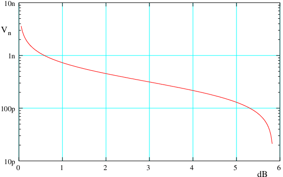
For very quiet amplifiers, we might use one resistor at room temperature and another immersed in liquid , at 77 K (Fig. 53). For a hypothetical noiseless amplifier, the Y-factor would be just the ratio of noise source temperatures, 293/77 = 3.8, corresponding to 5.8 dB, easily seen on a spectrum analyzer display with some averaging. Note that to get reasonably accurate results, the noise levels of the sources should be of a similar magnitude as that of the amplifier under test. This is apparent in figure 54, which plots the equivalent input noise voltage density against the Y-factor for the setup of figure 53 and where the slope of the curve increases at both ends. For higher noise levels, several instrument manufacturers propose calibrated noise sources with apparent noise temperatures in the 10 kK range.
Noise in matched amplifiers
If an amplifier is connected to a passive filter or a coaxial cable, it must have the correct input impedance, usually . If this is done with a simple resistor to ground (Fig. 55), the thermal noise of that resistor may turn out to be the main contributor to the total noise.
| (22) |

It’s possible to do better if we design the amplifier to have a largish negative gain , and to then use a feedback resistor from the output back to the input to set the terminating impedance (Fig. 56).
To keep the value of input impedance the same, must now be much larger: . The input referred noise voltage density due to the termination is now
| (23) |
much less than in Eq. (22). This is how a matched amplifier can have a very low apparent noise temperature, even though the whole circuit is kept at ordinary room temperature.

However, phase shifts and gain errors in the amplifier will affect , possibly to the point of making the input impedance go negative at some frequencies, causing instability with reactive sources. Additional measures must be taken to prevent that, for example by inserting constant-impedance low-pass elements (See §0.3.3).
An example of a low-noise amplifier stage
The design uses a JFET (BF862) input stage (Fig. 57). The voltage noise of the BF862 is specified as nV/. These being JFETs, the noise voltage is largely dominant over the contribution of the current noise at low source impedances, so we trade off one against the other by putting three JFETs in parallel, which brings down to 460 pV/. This also triples the parasitic capacitances, of which especially is troublesome, because its apparent value is multiplied by the gain of the JFETs (Miller effect). The deleterious effects of are limited by cascoding the JFETs with a BFT92 PNP transistor (T1).
The three 1 k resistors in the source leads of the JFETs set the DC current in each to 10 mA, which is the minimum guaranteed for this type. The transfer admittance at this current is about 35 mS per JFET, so 105 mS altogether. The collector load of the BFT92 is essentially the magnetization inductance of L4, about 5 mH. The open loop gain is then .
A final emitter follower NPN transistor T2 provides a sufficiently low output impedance to drive further stages. Gain-setting feedback is through the transformer composed of L1 to L4. This avoids the thermal noise that would have been introduced by feedback resistors. The turns ratio is 10, and so the gain in the feedback path is . The closed-loop gain is then , where is the open-loop gain. With appreciably larger than 10 above 10 kiloherz, the overall amplifier gain . Apart from yielding a flat, well defined gain over a large range of frequency, this feedback also considerably improves the amplifier’s linearity.
The transformer core is a tiny high-permeability amorphous metal toroid core that would saturate with only a few mA-turns of current. The DC bias current in the cascoding PNP transistor has been chosen to cancel the DC magnetization of the core due to the DC current of the JFETs.

The input impedance is set to by feedback through the 2k2 resistor. A 1:4 transmission line transformer brings that down to , doubling the gain and halving the input-referred voltage noise at the same time. A constant resistance bridged-T low-pass section hides the excursions of the input impedance near the high-frequency cut-off, keeping the amplifier stable at the same time.
The final result is an amplifier with 26 dB of gain, a bandwidth of 10 kHz to 75 MHz and a noise level of 260 pV/. This corresponds to an effective noise temperature of the amplifier of about 30 K, despite the fact that the amplifier is at room temperature.
The power supply lines are filtered using capacitance multipliers (T3, T4). Ordinary linear voltage regulators have noise levels of the order of 0.003% of the output voltage in a 10 kHz bandwidth, which seems very good until you realize that this is several thousand times the target noise level of the amplifier, and that this circuit does not by itself have a very good rejection of power supply noise. Capacitance multipliers reduce the noise density of the power supplies to more acceptable levels, of the order of a few nV/.
On the edge between noise and interference
Johnson and Schottky noise are fundamental noise sources. There are several more noise-like phenomena lurking in the dark. It depends on the application requirements if any of these are important. They often aren’t. Here are some things to keep in mind, in no particular order and without going into details. Temperature fluctuations caused by fans or turbulent airflow affect component values through their temperature coefficients. The Seebeck or thermoelectric effect causes small voltages to be developed when different metals are joined and are subjected to thermal gradients. Resistors and capacitors change value under mechanical stress and provide a path for acoustic noise to find its way in. Moreover, high-value ceramic capacitors may be piezo-electric. Carbon and cermet resistors suffer from excess noise, that is, noise over and above the Johnson noise, which manifests itself when a voltage is applied.
Semiconductors have 1/f noise, which becomes increasingly important at low frequency. Low noise transistors and integrated circuits usually have a 1/f corner frequency specification, below which this noise dominates all other sources. Semiconductors are also sensitive to light. Beware of components in translucent packages, such as glass diodes or ceramic-packaged transistors or ICs. Zener diodes above about 5 volts are actually avalanche diodes, which produce lots of noise, neither white nor Gaussian.
0.4.4 Grounding and Shielding, Interference
Interference can really spoil your day. Often it involves circuit elements that are assumed to be negligible such as the resistance of ground connections or cable screens, or the parasitic inductance of wires, resistors and capacitors.
It may be difficult to get a good model of the way interference couples into the signal. Usually, when the relevant coupling mechanism and the associated circuit elements have been identified, the solution to many EMC problems will be relatively straight-forward [20, 21].
Three coupling mechanisms need to be considered for interference mitigation. In no particular order:
- Common impedance coupling. High current paths should not share a conductor with low-level signals. Bear in mind that even a thick short straight wire has resistance and inductance. A sizable voltage can appear across its ends if the current is big enough or varies fast enough.


Consider the simplified power supply schematic of figure 59. The ground reference of the regulator shares a conductor with the rectifier reservoir capacitor. This wire or trace carries large current impulses which cause the regulator reference to jump, and the output voltage with it. Connecting the reference to the supply’s negative output terminal instead will result in a much quieter output voltage (Fig 59).
Star-point wiring, where all connections to a node meet at one point, is a common solution to common impedance coupling problems. However, it works well ony for low frequency. A full conductive plane works much better. Possibly, some slots or a peninsula may keep large currents away from sensitive areas, but you should avoid cutting up ground or power planes unnecessarily. Avoid running wires or PCB traces across slots.
- Inductive coupling. Current flows in closed loops. Minimize the area of loops with high . Keep wires with direct and return current close together. Use local bypass capacitors. Also identify nearby loops involving low-level signals. Keep those small too. Increase the distance between victim and aggressor loops. Magnetic shielding may help if the shield is correctly chosen and oriented. Static and low-frequency magnetic fields can be shielded with soft magnetic materials parallel to the field direction. High frequency fields are better shielded with eddy current shields normal to the magnetic field.
- Capacitive coupling (Fig. 60, left). Look for nodes with high . Keep those nodes small and close to a ground plane, to confine the fields. Put grounded screens around them. Reduce if possible. Also look for high impedance nodes, such as amplifier inputs and the like. Keep those nodes compact and far from the previous kind. Reduce the impedance, if possible. Keep them close to ground. Shield them (Fig. 60, right).

0.4.5 Radiation damage
Radiation affects mostly semiconductors [22]. The passive components are usually plenty radiation hard, except, maybe surprisingly, cables and connectors. Most contain PTFE, which is is a low-loss dielectric and doesn’t melt at soldering temperatures. Unfortunately, halogenated plastics deteriorate rapidly under irradiation and then exude corrosive emanations that attack nearby metal surfaces. Poor electrical contacts result. Paradoxically, it may be preferable to use connectors of the ’cheap and nasty’ variety, using polyethylene or polystyrene dielectrics, which hold up much better under irradiation.
The basic mechanism by which ionizing radiation damages semiconductors is that it dislodges atoms in the crystal structure, creating increased opportunities to scatter charge carriers, leading to an increased probability of recombination. The result is that bipolar transistor current gain is reduced progressively, mostly at low bias current levels.
There is no real substitute for measurement, but some sweeping observations can be made. Some transistors are more affected than others. Gold-doped transistors withstand many kilograys without deteriorating appreciably. General purpose small-signal transistors lose current gain exponentially, with decay constants in the 1 kGy ballpark. Lateral PNP transistors, used inside ICs, fail at low doses, because they already have low current gain to begin with and in addition, a large base region in which to capture damage. Such transistors are still used in a number of popular operational amplifiers and voltage regulators.
JFETs suffer increased leakage current of the gate junction. In MOSFETs, radiation ejects electrons from atoms in gate insulation layers, leaving trapped positive ions behind and causing a downward shift in threshold voltage. All these effects tend to reduce amplifier gain, increase noise and upset bias conditions.
The obvious path to rad-hard equipment design is to install as little as possible of the electronics in the irradiated area and to place what’s left out of harm’s way if at all possible. Other strategies are, of course, a judicious choice of components, to design your circuit to have largish standing currents and to tolerate large ranges of current gain or threshold voltage. An ample gain reserve, combined with the liberal application of feedback, helps to stabilize bias points and gain values.
In this context, note that older ICs are often more resilient because at the time of their conception, semiconductor processes did not allow close control of many circuit parameters, and designs were dimensioned to accommodate that. Newer designs rely on much narrower control of circuit parameters. They still drift under irradiation however, so these designs may have very poor radiation hardness.
Dynamic effects of radiation
Radiation can trigger brief current impulses in semiconductors, which may change the state of flip-flops or memory cells, so-called Single Event Upsets. The lesson is to avoid relying on state held in logic subject to radiation. Some remedial techniques might be to rewrite the logic state regularly from a remote location, or to use redundancy and error correction logic. For analog circuitry, there is really no other solution than to move it away.
Many integrated circuits can suffer from latch-up. This often involves parasitic components that aren’t shown in the device schematics, if such schematics are available at all. Latch-up is often destructive unless the circuit is somehow protected. This protection could take the form of compartmentalized and over-current-protected power distribution, possibly with latch-up detection and remediation circuitry.
Discrete designs are more robust against latch-up, because the parasitic elements that fragilize integrated circuits are absent in discrete components. ICs can be hardened by using semiconductor-on-insulator (SOI) techniques, which eliminate most of the troublesome parasitic circuit elements. Of course, these techniques are more costly.
0.5 Conclusion
Analog electronics has an important role to play in beam instrumentation. An instrument with a well-designed analog front-end will out-perform anything where this issue has been neglected. The problem facing beam instrumentation designers is the optimal extraction of a useful signal, which involves filtering, impedance and noise matching, amplification, transmission of signals over distances from decimeters to hectometers, rejection of interference, signal integrity, and radiation effects. Hopefully I have contributed something useful on these subjects.
References
- [1] P. Horowitz, W. Hill, The Art of Electronics, 3rd ed. Cambridge University Press 2015, ISBN 978-80926-9
- [2] P.C.D.Hobbs, Building Electro-Optical Systems, Making It All Work, Wiley 2009, ISBN 978-0470-40229-0
- [3] J. Williams (ed), Analog Circuit Design, Art, Science and Personalities, Butterworth-Heinemann 1991, ISBN 978-07506-9640-0
- [4] P.H. Smith, Transmission line calculator, Electronics, Vol.12, January 1939, pp29-31
- [5] C.L. Ruthroff, Some broad-band transformers, Proc. IRE, August 1959, pp1337-1342
- [6] J. Sevick, Transmission Line Transformers, Noble Publishing, Atlanta, GA, 2001.
- [7] G. Guanella, Nouveau transformateur d’adaptation pour haute fréquence, Revue Brown Boveri, September 1944, pp327-329
- [8] D.A. McClure, Broadband transmission line transformer family matches a wide range of impedances, RF Design, February 1994, p62-66, RF Design, May 1995, pp40-49
- [9]
J.M. Belleman, A Four-Decade Bandwidth Hybrid Coupler,
CERN-AB-Note-2006-005,
http://cds.cern.ch/record/927407 - [10] A.I. Zverev, Handbook of Filter Synthesis, Wiley 1967, ISBN 0471-98680-1
- [11] R. Saal, E. Ulbrich, On the design of filters by synthesis, IRE Transactions on Circuit Theory, Vol.5, Issue 4, December 1958, pp284–327
- [12] J.M. Belleman, Passive lowpass filters with constant input resistance, PS/BD/ Note 2002-193 (Tech.), http://cern.ch/jeroen/reports/crfilter.pdf
- [13] R.W. Rhea, Transforms aid the design of practical filters, Applied Microwave & Wireless, December 2001, pp36-44
- [14] C. Bowick, RF Circuit Design, Howard W. Sams & Company, ISBN 0672-21868-2
- [15] N. Balabian, T.A. Bickart, Electrical Network Theory, Wiley 1969, ISBN 0471-04567-4
- [16] G. Amsel, R. Bosshard, R. Rausch, C. Zajde, Time domain compensation of cable induced distortions using passive filters for the transmission of fast pulses, Rev. Sci. Instr. Vol. 42, No. 8, August 1971, pp. 1237-1246
- [17] J.B. Johnson, Thermal agitation of electricity in conductors, Physical Review, Vol. 32, July 1928, pp. 97-109
- [18] W. Schottky, Small-shot effect and flicker effect, Physical Review, Vol. 28, July 1926, pp. 74-103.
- [19] A.H. Haus, Description of the noise performance of amplifiers and receiving systems, Proc. IEEE, Vol. 51, March 1963, pp 436-442.
- [20] H. Ott, Noise-Reduction Techniques in Electronic Systems, 2nd ed., Wiley, New York 1988.
- [21] R. Morrison, Grounding and Shielding Techniques, 4th ed., Wiley, New York, 1998.
- [22]
M. Dentan,
Radiation effects on electronics components and circuits,
Part1, http://cern.ch/jeroen/coddampproto/Dentan1.pdf,
Part2, http://cern.ch/jeroen/coddampproto/Dentan2.pdf.