Circuit-model formulas for external-Q factor of resonant cavities
with capacitive and inductive coupling
Abstract
The external-Q factor of a resonant mode of a cavity represents the strength of the electromagnetic coupling between this resonant mode and the transmission mode of a waveguide coupled to the cavity. In this paper, we derive formulas to explicitly give the external Q of the cavities coupled with the waveguide through capacitive and inductive coupling. The derivation is based on the classical method that uses the reflection coefficient to estimate the coupling strength. Although the external Q is evaluated via three-dimensional computer simulations currently, these formulas may be useful for making speculations in the initial stages of cavity design.
I Introduction
The external-Q factor is a fundamental parameter of the cavity resonator; it determines the electromagnetic power radiated from the cavity to the waveguide. In the case of superconducting cavities, the external Q is especially important because the internal loss of rf power is negligible in comparison to the radiated power, and the bandwidth of the rf system is determined by the external Q. Therefore, it is essential to estimate the external Q while designing the cavity and rf system.
The standard method to evaluate the external Q is described in reference wei. This method uses the rf power radiated to the waveguide in addition to the cavity parameters to evaluate the external Q and coupling coefficient. It also provides an equivalent circuit of the cavity coupled with the waveguide. This treatment is widely used for the analysis of the cavity voltage because it precisely describes the electromagnetic field in the cavity.
However, the aforementioned method has the following two problems. First, this method only yields an equivalent circuit coupled with an ideal transformer. Therefore, the properties of the actual circuit, such as the input impedance and reflection coefficient, are not correctly represented. Second, the external Q can be obtained if only the input impedance, observed from the waveguide, is knownkam. In other words, the radiation power is not required to obtain the external Q.
A general method to calculate the external Q using the input impedance is given in reference kam, which, however, requires numerical calculation. Therefore, in this paper, we derive an explicit formulas to determine the external Q by another approach based on the reflection coefficient. We will see that the external Q are expressed in terms of the cavity parameters, through calculations of the refection coefficient for the two commonly used coupling schemes, i.e., capacitive and inductive coupling.
II Reflection coefficient and external Q

Let us suppose a general condition where a resonant cavity is coupled with a waveguide. The reflection coefficient represents a circle in the Smith chart around the resonance frequency, as shown in Fig. 1. We use this circle to obtain the coupling coefficient , which is defined by the ratio of the unloaded Q to the external Q, i.e.,
| (1) |
To this end, let the minimum and maximum absolute values of the reflection coefficient be and , respectively, as shown in Fig. 1. Note that the points corresponding to the minimum and maximum reflection coefficients are at opposite positions across the origin of the complex plane because is a circle. Then, the voltage standing wave ratios corresponding to the minimum and maximum values of are given by
| (2) |
and
| (3) |
respectively. According to reference sla, the coupling coefficient can be given by
Therefore, it is possible to obtain once and are known for a given cavity coupled with a waveguide.
III Capacitive coupling

Consider an LCR parallel resonant circuit coupled with a coaxial waveguide with a characteristic impedance through the coupling capacitance , as shown in Fig. 2. It represents an equivalent circuit of a cavity coupled capacitively with the waveguide. The resonance frequency and unloaded Q of the cavity are related to the circuit parameters as follows, respectively:
| (8) | |||||
| (9) |
In this paper, we assume that
| (10) |
The input impedance of the cavity at point P in Fig. 2 is given by the following equation.
| (11) | |||||
Here, we set
| (12) |
Let us define the second term of the last line of Eq. (11) by
| (13) |
This denotes the impedance of the parallel resonant circuit.
In this paper, the resonant cavities are treated with a very large , such as the superconducting cavities. In this case, it is sufficient to only consider the neighborhood of the resonance frequency; thus, the slowly changing factor in the first term of the right-hand side of Eq. (11) may be replaced with . Therefore, we consider the following equation instead of Eq. (11).
| (14) |
Here, we set
| (15) |
The real and imaginary parts of Eq. (14) are written as follows, respectively:
| (16) | |||||
| (17) | |||||
| (18) | |||||
| (19) |
The implications of these expressions are shown in Fig. 3, which plots and against . It is evident that the real part of coincides with the real part of . In contrast, the imaginary part of is shifted downward from the imaginary part of by .

Here, we assume that is very small in comparison to , i.e.11 1 We will see in the Appendix that this condition is fulfilled when Eq. (10) is valid.,
| (20) |
Under this condition, the equation or its equivalent quadratic equation,
| (21) |
has two roots, and , as schematically shown in Fig. 3, where they are defined as . Therefore, the following relationships are valid.
| (22) | |||||
| (23) |
It should be noted here that the input impedance is real at and . These real values at and are denoted by and , respectively. It is evident that the following relationships are also valid considering Eqs. (16) and (21).
| (24) | |||||
| (25) |
The value of is approximately zero, as shown in Fig. 3. Therefore, from Eqs. (22) and (23), we have
| (26) |
and
| (27) |
correspondingly22 2 We will consider the impedance matching condition in the Appendix.,
| (28) |
and
| (29) |
It is evident from Eq. (28) and assumption (20) that
| (30) |
Moreover, because the orders of and are similar to each other in the usual cavities, the following expression is also valid with a good approximation.
| (31) |

Now, let us consider the reflection coefficient of this circuit as observed from point P in Fig. 2 using the conditions obtained above. First, note that is a straight line in the complex -plane. This straight line is mapped to with two successive linear fractional transformations, namely, and . Therefore, certainly becomes a circle in the complex -plane. Second, by setting the reflection coefficient at as , we obtain the following approximation using Eqs. (29) and (10).
| (32) | |||||
In contrast, Fig. 3 shows that becomes approximately when moves away from to some extent. Thus, using Eq. (31), the approximate value of the corresponding refection coefficient can be given by
| (33) | |||||
In other words, the point with the largest reflection coefficient in this circuit is very close to the point corresponding to , which lies on the real axis, as shown in Fig. 4. Therefore, the following value may be used:
| (34) |
Consequently, the point with the smallest reflection coefficient should be very close to the point corresponding to , which is on the real axis, as shown in Fig. 4. In other words, the following approximation may be used:
| (35) |
This implies that
Thus, owing to the aforementioned results, the following approximated expressions can be obtained for the voltage standing wave ratio,
| (40) | |||||
Finally, we obtain the coupling coefficient by substituting these values in Eq. (II) as follows:
| (45) |
This expression is valid irrespective of the coupling strength. Moreover, owing to Eq. (1), the external Q can be given by
| (46) |
It should be noted is that the coupler tip (point P in Fig. 2) corresponds to the short end at the operating frequency when , as shown in Fig. 4.
IV Inductive coupling
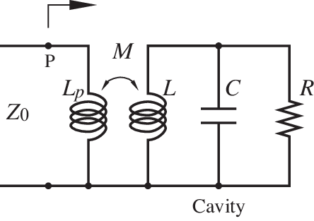
The cavities with inductive coupling can be treated in almost the same manner as those with capacitive coupling. Let us consider an inductively coupled circuit, as shown in Fig. 5, considering Eq. (10). The input impedance obsereved from point P in Fig. 5 leads to the following expression:
| (47) |
Because our consideration is limited in the neighborhood of , similar to the case of capacitively coupled circuit, we consider the following expression, where is replaced with in the first term of the right hand side of Eq. (47):
| (48) |
Note that the term is given by Eq. (15). The real and imaginary parts of in Eq. (48) are respectively given as follows:
| (49) | |||||
| (50) |
Figure 6 illustrates the implications of Eqs. (49) and (50).

Here, we assume that is very small in comparison to , i.e.,
| (51) |
Using the following expression,
| (52) |
this condition can also be written as33 3 This condition will be examined in the Appendix.
| (53) |
Under this condition, the equation has two roots, as shown in Fig. 6. We set the roots as and , where . They denote the solutions of the following quadratic equation:
| (54) |
Therefore, the following relationships are valid.
| (55) |
and
| (56) |
In contrast, the input impedance is real at and . We denote these real values at and by and , respectively. It is evident that the following relationships are also valid when we consider Eqs. (49) and (54):
| (57) | |||||
| (58) |
The value of is approximately zero, as shown in Fig. 6. Therefore, from Eqs. (55) and (56),
| (59) |
and
| (60) |
correspondingly44 4 We will consider the impedance matching condition in the Appendix.,
| (61) |
and
| (62) |
It can be observed from Eq. (62) and assumption (53) that
| (63) |
Moreover, because the orders of and are similar to each other in the usual cavities, the following expression also holds true with a good approximation:
| (64) |

By setting the reflection coefficient at as , we obtain the following approximation using Eqs. (61), (51), and (64):
| (65) | |||||
In contrast, Fig. 6 shows that when moves away from to some extent. Thus, using Eq. (64), the approximate value of the corresponding refection coefficient can be given by
| (66) | |||||
In other words, the point with the largest reflection coefficient in this circuit is very close to the point corresponding to , which lies on the real axis, as shown in Fig. 7. Therefore, the following value may be used:
| (67) |
Consequently, the point with the smallest reflection coefficient should be very close to the point corresponding to , which is on the real axis, as shown in Fig. 7. In other words, the following approximation may be used:
| (68) |
This implies that
Owing to these results, the following approximations can be obtained for the voltage standing wave ratio:
| (73) | |||||
Finally, we obtain the coupling coefficient by substituting these values in Eq. (II) as follows:
| (78) |
This expression holds true irrespective of the coupling strength. Moreover, owing to Eq. (1), the external Q can be given by
| (79) |
It should be noted that the coupler tip (point P in Fig. 5) also corresponds to the short end at the operating frequency when , as shown in Fig. 7.
V Summary
The external Q and coupling coefficient of the capacitively coupled resonant circuit shown in Fig. 2 can be represented by
| (80) |
and
| (81) |
respectively, where is the angular resonance frequency of the cavity.
The external Q and coupling coefficient of the inductively coupled resonant circuit shown in Fig. 5 can be represented by
| (82) |
and
| (83) |
respectively, where is the angular resonance frequency of the cavity and .
VI Acknowledgment
The way to understand the impedance behavior of a resonant circuit on the complex -plane, and the graphical representation of the impedance matching were suggested by Dr. Yoshiaki Chiba of RIKEN Accelerator Research Facility. The author would like to thank him for his guidance.
References
- (1) W. Weingarten,“Superconducting Cavities”, CAS - CERN Accelerator School: RF engineering for particle accelerators, CERN 92-03, p. 318 (1992).
- (2) O. Kamigaito,“Circuit-model representation of external-Q calculation”, Phys. Rev. ST Accel. Beams 9, 062003 (2006).
- (3) J. C. Slater, “Microwave Electronics”, Rev. Mod. Phys. 18, 441 (1946). Note that the definition of the voltage standing wave ratio in this paper is the inverse of Slater’s definition.
*
Appendix A Impedance matching
A.1 Capacitive coupling
First, we determine the impedance matching condition between a cavity and waveguide with the characteristic impedance through capacitive coupling. It is evident from Eqs. (16) and (19) that the matching condition can be obtained by changing such that the following relations may be fulfilled:
| (84) | |||||
| (85) |
By eliminating from the above equations, we obtain
| (86) |
This equation can determine the value of in the impedance matching problem.
A.2 Inductive coupling
In the case of inductive coupling, the matching condition contains two adjustment parameters, and , which relatively complicate the problem. Using Eqs. (49) and (50), the matching condition can be given by
| (88) | |||||
| (89) |
By eliminating from the above equations, we obtain
| (90) |
This equation can determine the value of and in the impedance matching problem. To achieve a matching condition when , the following expression must be valid, unless is too large:
This is Eq. (64). Under these conditions, the first term in the left-hand side of Eq. (90) can be neglected to obtain
| (91) |
This implies that Eq. (53) is valid.