Timing resolution of a plastic scintillator counter read out by radiation damaged SiPMs connected in seriesJournal: NIM-A
Abstract
This paper discusses the effects of radiation damage to SiPMs on the performances of plastic scintillator counters with series-connected SiPM readout, focusing on timing measurements. The performances of a counter composed of a scintillator tile read out by two sets of six SiPMs from AdvanSiD connected in series attached on the short sides are presented, for different combinations of SiPMs at various levels of irradiation. Firstly, six SiPMs were equally irradiated with electrons from 90Sr sources up to a fluence of . The timing resolution of the counter gradually deteriorated by the increase in dark current. The dark current and the deterioration were reduced when the counter was cooled from 30∘C to 10∘C. Secondly, 33 SiPMs were irradiated with reactor neutrons. The characteristics of counters read out by series-connected SiPMs with non-uniform damage levels, were investigated. The signal pulse height, the time response, and the timing resolution depend on the hit position in the counter, when SiPMs’ irradiation is not uniform.
Keywords:
Radiation tolerance , Series connected SiPMs , Timing resolution , Scintillator detector1 Introduction
Scintillator detectors read out by Silicon PhotoMultipliers (SiPMs) are used in a wide range of experiments to detect charged particles in particular when high timing resolution is required. Series connection of SiPMs is found to be effective to achieve high timing resolutions [1], because it reduces the SiPMs’ total capacitance and therefore reduces the rise time of the output signal. Examples are the pixelated Timing Counter (pTC) in the MEG II experiment [2], the electromagnetic calorimeter in the Mu2e experiment [3], and the TOF detector in the PANDA experiment [4].
Many studies on irradiation damage on SiPMs are available (recent studies are summarised in [5]). Nevertheless, a detailed study on its effect on the timing resolution of scintillator counters read out by series-connected SiPMs has not been presented yet. In this work, the effect of radiation damage to SiPMs on the performance of a counter consisting of a scintillator tile read out by two sets of six series-connected SiPMs on opposite sides is investigated, focusing on the timing resolution. First, the effect of the increase in dark current is investigated with six equally-irradiated SiPMs. Next, additional impact on timing measurements due to non-uniformity of irradiation is investigated with several combinations of differently-irradiated SiPMs. In an experimental setup non-uniform damage among series-connected SiPMs can occur if the hit rate in the counter depends on the position of the SiPMs.
2 Radiation damage to SiPMs and series connection
2.1 Radiation damage to silicon sensors
Collisions of energetic particles with silicon bulk cause displacement of the atoms, i.e. lattice defects. This bulk damage can be classified into two types: point defects and cluster defects. Their relative weight depends on the type and the energy of incident particles. Low energy electrons, such as those from 90Sr sources (maximum energy at 2.28 MeV from cascade 90Y decay), mainly produce point defects while hadrons such as 1-MeV neutrons produce cluster defects. More energetic electrons with energy produce both types with the relative weight of cluster defects increasing with the energy.
One of the major effects of the bulk damage to the sensor characteristics is an increase in bulk dark current. Therefore, the damage level is often quantified using the dark current increase. In case of SiPMs, the bulk dark current undergoes multiplication and results in dark counts, which are indistinguishable from light-induced counts, that may degrade timing measurement.
2.2 Scintillator counters with series-connected SiPMs readout
The series connection of multiple SiPMs shows some peculiar features. When SiPMs are connected in series, the total sensor capacitance reduces by a factor of , while the effective charge gain of each SiPM also reduces by the same factor. The voltage needed to apply the same bias voltage to each SiPM becomes times higher. A common current flows through all the SiPMs and balances the bias voltages among the SiPMs. As in the case of parallel connection, not only the photon statistics but also the dark counts are summed.
Sect. 2.2.1 presents the pTC in the MEG II experiment because the design of our test counter is based on the design of a pTC counter.
2.2.1 MEG II pTC
The MEG II pTC, dedicated to measuring the timing of positrons from muon decays, is composed of 512 plastic scintillator counters. A single counter is a two-side readout plastic scintillator (BC422) with dimensions of ; each side is read out by six series-connected SiPMs with cell size and active area11 1 ASD-NUV3S-P High-Gain from AdvanSiD.. Each side detects roughly 50–100 photoelectrons, depending on the scintillator light yield and the photo-detection efficiency (PDE) of the SiPMs, achieving 70–90 ps timing resolution with the two-side measurement.
The pTC was operated in pilot runs of the MEG II experiment for a month using the nominal intensity positive muon beam () [6]. During the beam time, an increase in the SiPMs’ dark currents was observed. By linearly extrapolating the increase to the planned three-year data-taking period, the dark currents, a few before the exposure, are expected to reach on average at the operating bias voltages at 30∘C. The positron flux was measured by the counters. It depends on the position of the counters; the counters at the highest hit-rate region ( kHz) will be exposed to of MeV positrons with an absorbed dose of Gy in the three-year run. The total fluence roughly corresponds to the 1-MeV neutron equivalent fluence , converted by using an “effective NIEL” calculated using molecular dynamics simulations [7]. The fluence is not uniform inside a counter. It depends on the distance from the beam axis, and the inner-most SiPM will be exposed to roughly triple the flux compared to that of the outer-most SiPM. Preliminary results on the effects of radiation damage were reported in [8].
3 Experimental setup
3.1 Samples and irradiation
SiPM samples (ASD-NUV3S-P High-Gain) were irradiated with electrons and neutrons at different fluences. ASD-NUV3S-P High-Gain is based on a p-on-n structure for detection of near ultraviolet light and the properties are summarised in Table 1.
| Parameter | Value |
|---|---|
| Active area11 1 From AdvanSiD data-sheet. () | |
| Cell size11 1 From AdvanSiD data-sheet. () | |
| Peak sensitivity wavelength11 1 From AdvanSiD data-sheet. (nm) | |
| Breakdown voltage11 1 From AdvanSiD data-sheet. (V) | |
| Gain11 1 From AdvanSiD data-sheet. (at V) | |
| Quench resistance22 2 Measured value [9]. (M) | |
| Recharge time constant22 2 Measured value [9]. (ns) |
Electron-irradiated samples
Six SiPMs (#1–#6) were irradiated to the same fluence using two 37-MBq sources. The irradiation was separated into four steps, each 70 hours long. The two sources were swapped alternately between each step to irradiate uniformly all the samples. During the irradiation, no bias voltage was applied to the SiPMs. Between the steps, the measurement described in Sect. 3.2 was performed. The total fluence in the 280-hour exposure was measured to be with a total dose of 1 kGy,22 2 The total dose was evaluated with a simulation based on Geant4. equivalent to using the effective NIEL value [7].
Neutron-irradiated samples
A set of 33 SiPMs was irradiated with neutrons with kinetic energies ranging from 0.5 MeV to 16 MeV using the reactor neutron facilities at the Laboratory of Applied Nuclear Energy (LENA) of the University of Pavia. The set was divided into sub-groups for different fluence levels ranging from to . The 1-MeV neutron equivalent fluences were calculated from the differential neutron flux of the reactor following [10]. Among them, two samples with (#7, #8) and two with (#9, #10) were used in this study.

3.2 Timing measurements
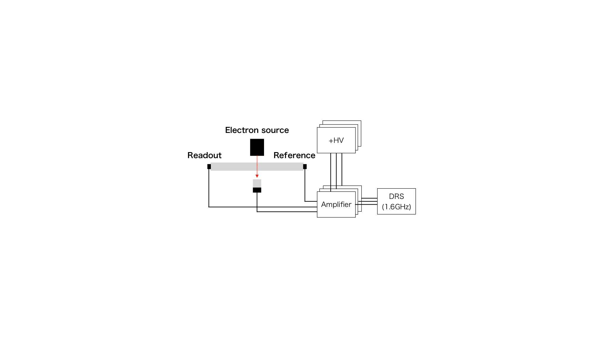
The main topic of this paper is the measurement of the timing resolution of a counter equipped with irradiated SiPMs. Figure 1 shows the measurement setup. The counter consists of a scintillator tile (BC422), whose scintillation photons are read out by six series-connected SiPMs on each short side: on one side, the SiPMs under test and, on the opposite one, non-irradiated SiPMs as reference. The tile and the SiPMs are coupled with optical grease and are aligned through a custom-made jig produced with a 3D printer. The electrical contacts with the SiPMs33 3 They are surface-mount type. are made by means of spring probe pins so that the series circuit can be made each time without soldering.
A 3.7-MBq source emitted electrons into the counter. The trigger signals were generated by a scintillator (BC422) trigger counter read out by one SiPM (Hamamatsu Photonics S10362-33-050C), located under the scintillator. A fraction of the electrons is energetic enough to reach the trigger counter and release energy sufficient to fire the trigger.
The trigger counter has a much better timing resolution ( ps) than the test counter [1], and therefore, its timing measurement () can be used as a reference of the electron hit timing on the test counter (). The time response of the six series-connected SiPMs under test was characterised by the mean value of distribution, or “time centre”, and the timing resolution from its standard deviation .44 4 The counter resolution becomes times better with the two-side readout.
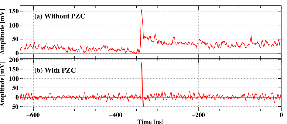
The output signals were amplified and shaped through a two-staged voltage amplifier with a pole-zero cancellation (PZC) filter, shown in Fig. 2. Figure 3 shows typical waveforms after irradiation with and without PZC. The baseline is stabilised by the filter and the dark count effect on the timing measurement is significantly suppressed. The PZC is effective for a good timing measurement especially under high dark count rate condition. In this study, the PZC was always active.
The signal waveforms were recorded using the Domino Ring Sampler waveform digitiser (DRS4) [11], at a sampling speed of 1.6 GS/s. The pulse timing was measured through the digital constant fraction discriminator method (CFD) with a cubic interpolation between the sampling points.
Some parameters of SiPMs have significant temperature dependence. Therefore, the measurements were performed at 30∘C and 10∘C to evaluate the effect of the operating temperature.
4 Dark current measurement and timing resolution
4.1 I-V curves


Figures 4–4 show the dark current versus reverse bias voltage (I-V) curves of each of the six electron-irradiated SiPMs and Figs. 4–4 show the I-V curves when they are connected in series (taken at 0.1 V steps). The breakdown voltage is calculated from the maximum point in the second-derivative of the logarithm of with three-point smoothing [12] and the systematic uncertainties are estimated from the change by different smoothing. Table 2 summarises the breakdown voltages and confirms that the sum of the single breakdown voltage values is consistent with the value from those connected in series when values are similar among the SiPMs.
| SiPM | (V) |
|---|---|
| #1 | 24.32 0.03 |
| #2 | 24.31 0.03 |
| #3 | 24.38 0.04 |
| #4 | 24.38 0.03 |
| #5 | 24.32 0.04 |
| #6 | 24.39 0.03 |
| Sum of #1 - #6 | 146.1 0.2 |
| #1 - #6 Connected in Series | 146.21 0.05 |
The dark currents increase significantly under electron irradiation; roughly by one order of magnitude below the breakdown voltage and two orders of magnitude above it. On the other hand, the breakdown voltages are only marginally affected by the electron-irradiation damage as shown in Fig. 4. The systematic difference between non-irradiated and irradiated points could be due to the algorithm for the determination because the slope of the current after the breakdown becomes steeper after the first irradiation.
4.2 Waveforms
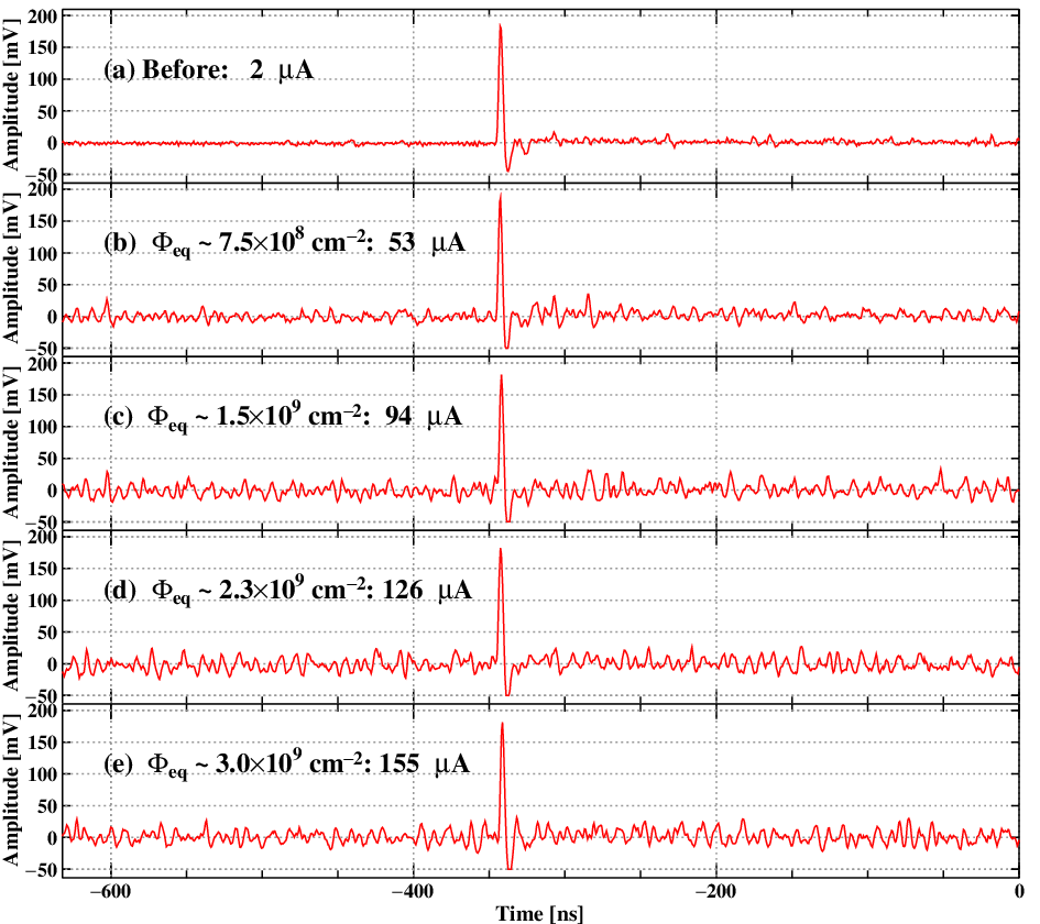
Figure 5 shows an example of the waveform from the series-connected SiPMs with the electron-irradiated samples at each irradiation step. The fluctuation of the baseline increased significantly as shown in Fig. 6, where is the mode value of RMS noise calculated with baseline points before the signal region.

4.3 Timing resolution

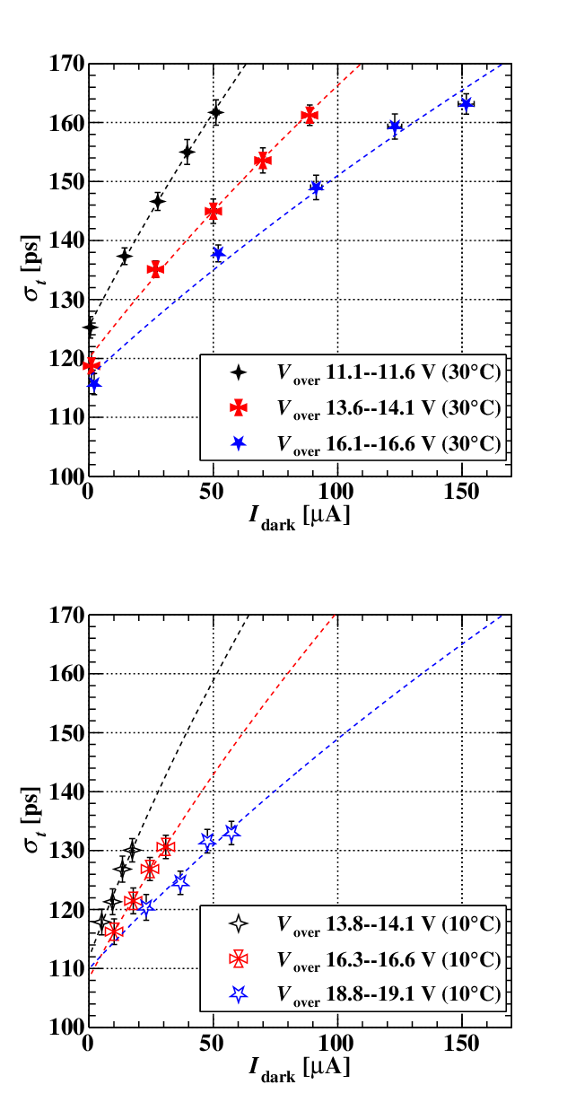

The timing resolution is optimised scanning the bias voltage in the range V ( V), in steps of 2.5 V both at 30∘C and 10∘C. The data were analysed with a fixed CFD fraction of 20% and the results are shown in Fig. 7. The resolution first improves with due to a higher gain and PDE, but at some voltage starts to deteriorate due to increased dark counts. As the fluence increases, the optimal voltage, where reaches the minimum, shifts to lower voltages. at each optimal voltage gradually worsens and after the fourth irradiation the degradation reaches %.
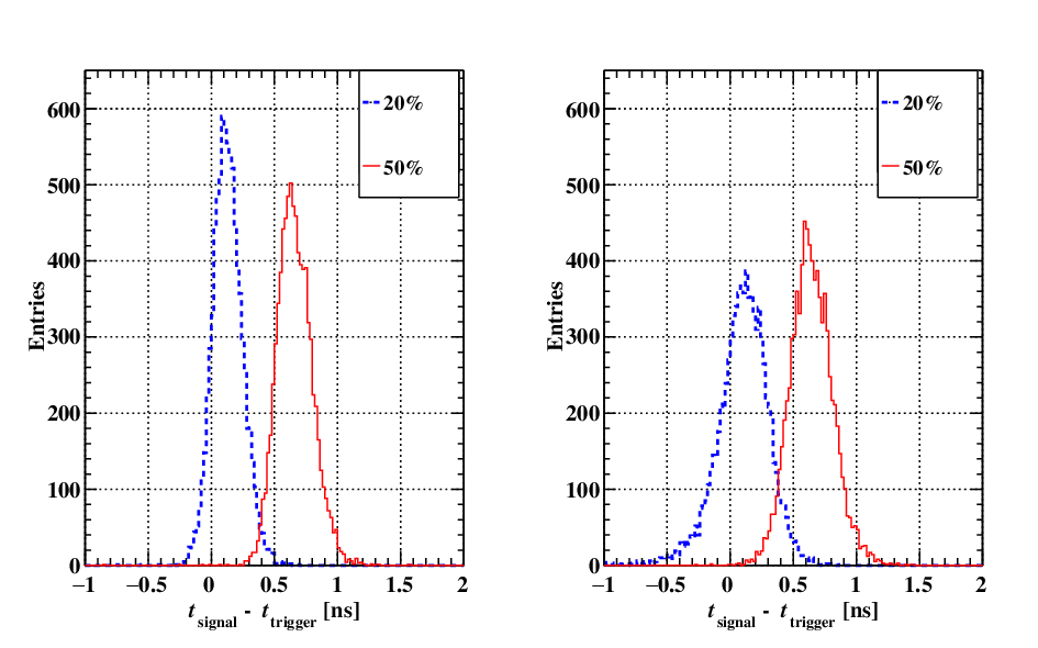
Next, three points around each optimal voltage ( = 157.5, 160.0, 162.5 V) are selected, , 14.0, 16.5 V for the 30∘C datasets and , 16.5, 19.0 V for the 10∘C datasets, and the CFD fraction is optimised in steps of 10% from 10% to 60% for each dataset. Figure 8 shows the distribution of the calculated timing after irradiation with different CFD fractions at V (30∘C). As the noise increases, the optimal fraction value becomes higher: from 20% to 50%.
Figure 9 shows the relation between and . When the dark current increases to , deteriorates by % at V.
Compared to the 30∘C case, is significantly lower at 10∘C at each irradiation step. Comparing the two cases at V after 140-hour irradiation (the third black marker at 30∘C and the second white marker at 10∘C in the plot), the dark current decreases from to and the deterioration of the timing resolution reduces from % to %.
The dependence of can be explained by the relation between and . The signal height was constant during these measurements within the range of the measurement errors ( 0.15 – 0.16 V from the most-probable value of its Landau-like distribution). Figure 10 shows the relation between and . can be expressed by the square root of the square sum of the intrinsic timing resolution () and the additional fluctuation from the noise (). Also, can be scaled by the dependence as shown in Fig. 6. Hence the deterioration of can be described by dependence.
5 Series connection of differently damaged SiPMs
The previous section presents the relation between and of a scintillator counter with equally-irradiated series-connected SiPMs. Under more realistic assumptions, SiPMs may be irradiated with different fluences due to position dependence of the particle flux. In the following, results with differently-irradiated SiPMs connected in series are presented.
5.1 Patterns of SiPM combination

The combinations of SiPMs used for this test are:55 5 Here the SiPMs are distinguished not by the kind of irradiating particles but only by the current level.
- 1.
Pattern A is composed of two electron-irradiated () SiPMs (#1 and #2 [or #5]66 6 SiPM #2 was broken during the measurement and was replaced with #5, which has the same damage level and I-V characteristics as #2.) and four non-irradiated SiPMs (#11–#14).
- 2.
Pattern B is composed of four electron-irradiated () SiPMs (#1–#4 [#5]) and two non-irradiated SiPMs (#11, #13).
- 3.
Pattern C is composed of two electron-irradiated SiPMs (#1, #2 [#5]) and four neutron-irradiated SiPMs, two with the fluence level of samples (#7, #8) and the other two with ones (#9, #10).
- 4.
Pattern D is composed of six electron-irradiated () SiPMs (#1–#6). They are the same SiPMs used in Sect. 4.
Pattern A and pattern B are considered as extreme cases to highlight the effects of differential irradiation, while pattern C simulates a gradient damage level closer to a realistic condition.
The coordinate system on the tile is defined such that the -axis runs along the long direction while the -axis runs along the short direction with the origin point at the centre of the tile. The SiPMs under test are located at the negative side; the signal is extracted from the positive side, while the negative side is connected to the ground line. The more highly-damaged SiPMs were located at larger position: this configuration of SiPMs is called “normal order". Data were taken also with SiPMs ordered in the opposite way along the direction: this configuration is called “reverse order". Figure 11 illustrates the layout of each pattern.
5.2 I-V curves and apparent breakdown voltage shift
Figures 17–17 show the I-V curves of individual SiPMs used in patterns A, B, and C. Figures 17 and 17 show the I-V curves of them in series measured at 30∘C and 10∘C, respectively. The breakdown voltages of patterns A and B turned out to be shifted to values higher than that of pattern D. Table 3 shows the breakdown voltage values of pattern A , pattern D, and the SiPMs used for those patterns.
When the I-V characteristics of series-connected SiPMs differ, the applied voltage to each SiPM is adjusted to accommodate a common current. As a consequence, the over-voltages for the six SiPMs differ from one another; even when the total applied voltage is below the apparent breakdown voltage, voltages applied to non-damaged SiPMs may result to be higher than their breakdown voltages (positive over-voltages) to accommodate the same dark current as that of the damaged SiPMs below the breakdown (negative over-voltages). This mechanism causes an apparent breakdown voltage shift depicted in Figure 17.
| SiPM | (V) |
|---|---|
| #1 (30∘C) | 24.20 0.03 |
| #2 (30∘C) | 24.23 0.03 |
| #3 (30∘C) | 24.29 0.03 |
| #4 (30∘C) | 24.28 0.03 |
| #5 (30∘C) | 24.23 0.03 |
| #6 (30∘C) | 24.30 0.03 |
| #11 (30∘C) | 24.28 0.03 |
| #12 (30∘C) | 24.33 0.03 |
| #13 (30∘C) | 24.39 0.03 |
| #14 (30∘C) | 24.32 0.03 |
| Sum of #1 - #6 | 145.5 0.2 |
| Sum of #1, #2, #11 - #14 | 145.7 0.2 |
| Pattern D (30∘C) | 145.94 0.05 |
| Pattern A (30∘C) | 147.51 0.05 |
| Pattern D (10∘C) | 143.43 0.05 |
| Pattern A (10∘C) | 144.89 0.05 |


5.3 Bias voltage scan at centre


First, from the over-voltage scan data with the measurement setup presented in Sect. 3.2 the pulse height and the timing resolution were evaluated. Figures 18 and 19 shows the results. The pulse height is defined as the most-probable value of its Landau-like distribution. Although over-voltages from the apparent breakdown voltages become smaller, the pulse heights remain constant as in pattern D; that is, the total effective over-voltages remain constant. The timing resolution is recovered again by cooling.
5.4 Hit position dependence in a counter
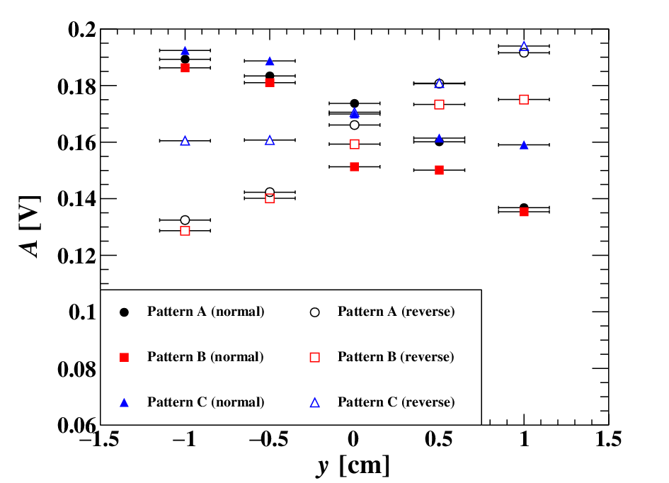
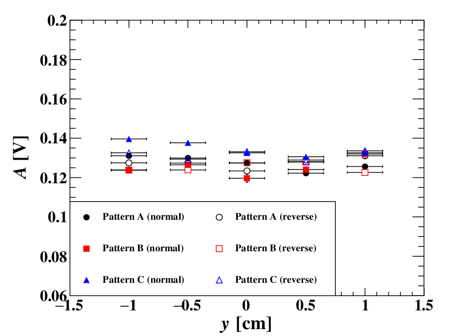
Next, the dependence of various variables on hit position in counters was examined.77 7 In this subsection, the pulse height and the noise situation were changed from the measurements in Sect. 4.3 and 5.3 due to a change in the setup. However, those parameters were stable during each measurement, and so the position dependence in different damage patterns can directly be compared. Data were taken at different positions in the range of and in the normal order. Then, the measurements were repeated in the reverse order to clearly distinguish the effect of radiation damage from other effects.
Pulse height
Figure 21 shows the dependence of the pulse height on -position at . A clear dependence is observed, and the slope is opposite for the normal and the reverse order cases, clearly indicating the effect of the position-dependent damage to SiPMs. When the illuminated point is close to more-damaged SiPMs the pulse height becomes smaller since the damaged SiPMs, which detect a large fraction of scintillation light in this case, have smaller gain due to the smaller over-voltages.
When the illuminated points move far from the SiPMs, the dependence of the pulse height decreases and at cm, the dependence becomes almost flat as shown in Fig. 21.
Time centre
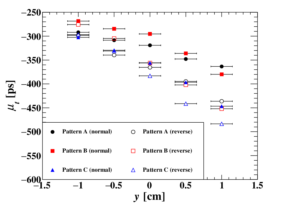
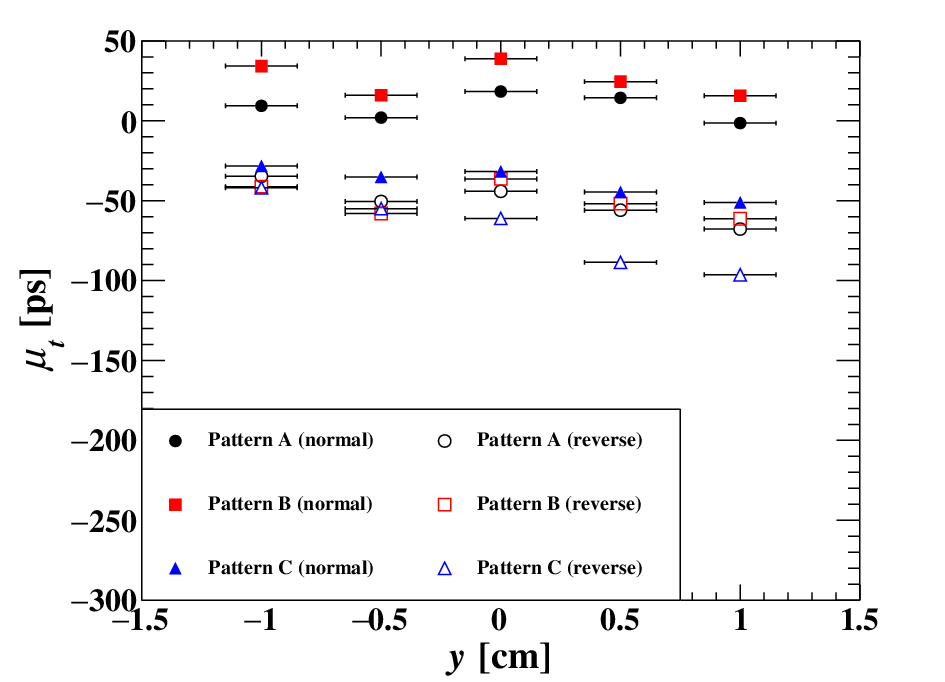
Figures 23 and 23 show the time centre at cm and cm, respectively. Similar -dependencies are observed in all the damage patterns at cm. For this variable, however, the results of normal- and reverse-order show the same sign of the slope, while the magnitudes of the slope are different. The mechanism yielding the dependence is more complex than that for pulse height because the signal timing in the CFD method is determined by multiple factors: the distribution and arrival time of photons to each SiPM, the gain of each SiPM, the time response of each SiPM, and the signal propagation time along the series-connected SiPMs.
The common trend stems from a finite propagation time of the scintillation light in the scintillator and the electronic signal through the series-connected SiPMs. Because of the read out from side, signals from higher hits are detected earlier than those from lower hits. This interpretation is confirmed by a measurement using non-irradiated SiPMs.
Deviations from the common trend suggest the effect of radiation damage but the non-uniform radiation damage complicates matters because of the over-voltage variation among the SiPMs, affecting both the gain and the time response. To measure the relationship between the over-voltage and the time response, the over-voltage dependence of the time centre for the all-non-damaged case and the all-damaged case is measured. Because of the limited number of non-damaged samples, this measurement was performed using four SiPMs in series. The result is shown in Fig. 24. Both damaged and non-damaged SiPMs show a faster time response with higher over-voltage, although it saturates at some point. This suggests faster buildup and propagation of avalanche in a stronger electric field [13, 14]. Due to the dependence of on , SiPMs with less damage in a chain output faster signals than the ones with more damage.
A qualitative explanation for the difference between the normal and the reverse order is the following. The measurement of the timing at the 20% CFD fraction samples the leading edge of the pulse. The main contribution to this part comes from few SiPMs closest to the signal readout line (i.e. side), especially when the hit point is at higher . In the normal order case, these SiPMs yield smaller and slower signals and thus the time centre is larger than that in the reverse order case. When the hit point is at lower , a smaller fraction of the scintillation light is collected by these SiPMs and signals from successive SiPMs contribute more to the CFD timing. This weakens the effect of the position-dependent damage. Therefore, similar time centre values are obtained in the two cases. As a general trend, the normal order yields less position dependence than the reverse order since the position-dependent damage effect compensates the common trend. The position dependence is mitigated when the fraction of CFD is increased.
When the illuminated point moves far from the SiPMs, the position dependence in -direction becomes gradually decreases.

Timing resolution
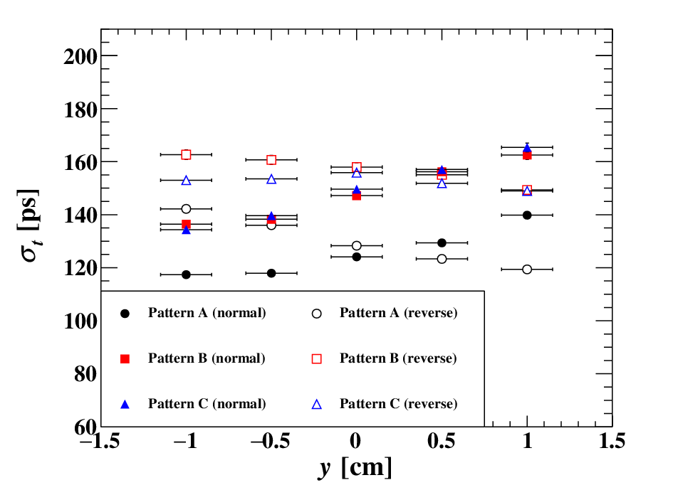
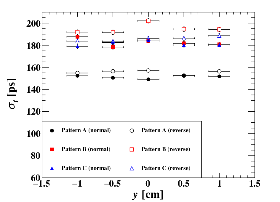
Figures 26 and 26 show the position dependence of the timing resolution at and , respectively. The flipped behaviour between the normal and the reverse order cases is due to the timing resolution predominantly depending on the signal-to-noise ratio. It becomes worse when the illuminated point is close to the damaged SiPMs.
The data show slightly better resolutions in the normal order than in the reverse order. This may indicate a second-order effect on the timing resolution from the combination of SiPMs with different time responses. As discussed in Sect. 5.4, the normal order connection compensates the dispersion of signal timings measured by different SiPMs, resulting in a better resolution.

6 Discussion
The timing resolution is predominantly determined by the signal-to-noise ratio. Irradiation induces an increase in and causes deterioration of ; the deterioration is described by the square root of dependence. This indicates that in a running experiment can be estimated in real time by monitoring .
As expected, cooling helps to reduce the impact of the radiation damage on . Because of limitations in the setup, the only tested temperature was 10∘C. Cooling down to lower temperatures further reduces the impact or enables operation in a harsher environment, although it imposes additional constraints, such as thermal insulation and dehumidification, on the detector design. In addition, re-optimisation of and the CFD fraction values depending on the damage level turns out to be effective in mitigating the deterioration of .
Annealing of SiPMs can be another way to recover the original . However, if the SiPMs are glued to the scintillator with optical cement, the applicable temperature is limited to well below 70∘C, at which the scintillator melts.
A study on connecting differently-damaged SiPMs in series was performed in [3], which reports the measurement of the charge for laser light readout by three SiPMs connected in series: two of them were non-damaged and one was extensively damaged. The present study extends it systematically and quantitatively to find additional effects on the operation and performance of scintillator counters.
An apparent breakdown-voltage shift is found, which is a phenomenon peculiar to the series connection of differently-damaged SiPMs, spoiling the determination of the effective breakdown voltage from the I-V characteristics. Monitoring the operating over-voltage is important for long-term data taking. Therefore, this phenomenon should be monitored during the operation of detectors in a real experiment.
As a whole, counters equipped with differently-damaged SiPMs work as properly as those with equally-irradiated SiPMs. The pulse height does not change on average and the timing resolution is similar to that of equally-irradiated SiPMs with the equivalent damage level. These can be an advantage of the series connection over parallel connection. In parallel connection, each SiPM has a fixed over-voltage, leading to the same pulse height, however, the currents are highly non-uniform among the SiPMs, and the operating voltage and the timing resolution can be limited.
A drawback of the series connection is the position dependence of the pulse height, the time centre, and the timing resolution, which can be avoided in the case of parallel connection by a careful design of the circuit. The dependence of the pulse height is peculiar to the case with differently-damaged SiPMs, while that of the time centre stems from a combination of an intrinsic property of series connection and effects of the different damage levels. The intrinsic one observed in this study is in contrast to the result reported in [1]. The difference could be due to the different sizes of the scintillator tile and different numbers of SiPMs in series.
The variation of the time centre in a counter results in a biased time reconstruction depending on the hit position, and thus, this additional spread in the measured time worsens the timing resolution. If the hit position information is available, e.g. from an external tracker, the dependence can be corrected. The dependence changes with different damage levels and the combination of SiPMs. Therefore, the position dependence of the time centre should be monitored during an experiment. The normal order, i.e. extracting signal from the higher damage side, is better because it yields less position dependence than the reverse order. Cooling does not help to reduce the position dependence because the difference of over-voltages between the damaged SiPMs and non-damaged SiPMs does not decrease even when the SiPMs are cooled as shown in Fig. 27 and Table 3.
Impact on MEG II pTC
The single-counter deteriorates of 41% by the increase in at V (30∘C) after irradiation of , which is equivalent to the average damage level in the MEG II three-year run. This deterioration is reduced to 13% by cooling the setup to 10∘C. The pTC system is equipped with a water chiller system, which can control the detector temperature in the range – C while it is expected to be C without it. The MEG II collaboration adopted 10∘C as the operating temperature of the pTC.
The closest approximation to the damage in the pTC channels is pattern C since the positron flux is larger at smaller radius. Unfortunately, the pTC was designed with the readout from the larger radius side, which corresponds to the reverse order case in this study, and all the counters have been already assembled. A -dependence of is expected at cm. The external tracking detector will be available to estimate the hit -position. Therefore, a correction for the time centre dependence can be applied and the deterioration can be, at least partially, compensated.
7 Conclusions
The effect of radiation damage to SiPMs on the performances of a scintillator counter with series-connected readout was studied using ASD-NUV3S-P High Gain SiPMs irradiated either with electrons from 90Sr sources up to or with neutrons from a reactor up to . The increase in dark count rate is the main cause of the timing resolution deterioration. Reducing the dark count rate by cooling the SiPMs effectively recovers the timing resolution. Position dependencies of the pulse height, the time centre and the timing resolution are observed when the series-connected SiPMs have different I-V characteristics. The time centre dependence on the hit position results in additional degradation of the timing resolution. When the damage level is not uniform within the series-connected SiPMs, the time centre depends also on the direction of the signal line. The best timing resolution is obtained by reading the signal from the side where the most heavily damaged SiPMs are located. Furthermore, a shift of the apparent breakdown voltage is observed, which might spoil the determination of the effective breakdown voltage from the I-V curve.
Acknowledgments
We thank PSI as the host laboratory, and we thank Arnold Marcel from the PSI group who helped us to calculate the source activities. We thank the Laboratorio Energia Nucleare Applicata (LENA) in Pavia and in particular Alloni Daniele, Prata Michele, and Salvini Andrea for the irradiation of SiPMs with neutrons. This study was supported by INFN, JSPS KAKENHI Grant Numbers JP26000004, JP19J13635, and JSPS Core-to-Core Program, A. Advanced Research Networks JPJSCCA20180004.
References
- [1] P. W. Cattaneo et al., Development of high precision timing counter based on plastic scintillator with SiPM readout, IEEE Trans. Nucl. Sci. 61 (2014) 2657–2666, https://doi.org/10.1109/TNS.2014.2347576.
- [2] A. M. Baldini et al., The design of the MEG II experiment, Eur. Phys. J. C (2018) 78:380, https://doi.org/10.1140/epjc/s10052-018-5845-6.
- [3] N. Atanov et al., The Mu2e calorimeter final technical design report, arXiv:1802.06341
- [4] M. Böhm et al., Fast SiPM readout of the PANDA TOF detector, 2016 J. Instrum. 11 C05018, https://doi.org/10.1088/1748-0221/11/05/c05018.
- [5] E. Garutti, Yu. Musienko, Radiation damage of SiPMs, Nucl. Instrum. Methods A 926 (2019) 69–84, https://doi.org/10.1016/j.nima.2018.10.191.
- [6] M. Nakao et al., Results from pilot run for MEG II positron timing counter, Springer Proc. Phys. 213 (2018) 237–241, https://doi.org/10.1007/978-981-13-1316-5.
- [7] C. Inguimbert, P. Arnolda, T. Nuns, G. Rolland, “Effective NIEL” in silicon: calculation using molecular dynamics simulation results, IEEE Trans. Nucl. Sci. 57 (2010) 1915–1923, https://doi.org/10.1109/TNS.2010.2049581.
- [8] M. Usami et al., Radiation damage effect on timing resolution of 6 series-connected SiPMs for MEG II positron Timing Counter, Nucl. Instrum. Methods A 936 (2019) 572–573, https://doi.org/10.1016/j.nima.2018.10.053.
- [9] Y. Uchiyama et al., 30-ps time resolution with segmented scintillation counter for MEG II, Nucl. Instrum. Methods A 845 (2017) 507–510, https://doi.org/10.1016/j.nima.2016.06.072.
- [10] ASTM Standard E722-93, Standard practice for characterizing the neutron energy fluence spectra in terms of an equivalent monoenergentic neutron fluence for radiation-hardness testing of electronics, in: 1993 Annual Book of ASTM Standards, Vol. 12.02, ASTM International, West Conshohocken, PA, 1993, pp. 324–337.
- [11] S. Ritt, R. Dinapoli, U. Hartmann, Application of the DRS chip for fast waveform digitizing, Nucl. Instrum. Methods A 623 (2010) 486–488, https://doi.org/10.1016/j.nima.2010.03.045.
- [12] M. Simonetta et al., Test and characterisation of SiPMs for the MEGII high resolution Timing Counter, Nucl. Instrum. Methods A 824 (2016) 145–147, https://doi.org/10.1016/j.nima.2015.11.023.
- [13] A. Lacaita, M. Mastrapasqua, M. Ghioni, S. Vanoli, Observation of avalanche propagation by multiplication assisted diffusion in - junctions, Appl. Phys. Lett. 57 (1990) 489–491, https://doi.org/10.1063/1.103629.
- [14] A. Spinelli, A. L. Lacaita, Physics and numerical simulation of single photon avalanche diodes, IEEE Trans. Electron Devices 44 (1997) 1931–1943, https://doi.org/10.1109/16.641363.