Run-Time Accuracy Reconfigurable Stochastic Computing for Dynamic Reliability and Power Management
Abstract
In this paper, we propose a novel accuracy-reconfigurable stochastic computing (ARSC) framework for dynamic reliability and power management. Different than the existing stochastic computing works, where the accuracy versus power/energy trade-off is carried out in the design time, the new ARSC design can change accuracy or bit-width of the data in the run-time so that it can accommodate the long-term aging effects by slowing the system clock frequency at the cost of accuracy while maintaining the throughput of the computing. We validate the ARSC concept on a discrete cosine transformation (DCT) and inverse DCT designs for image compressing/decompressing applications, which are implemented on Xilinx Spartan-6 family XC6SLX45 platform. Experimental results shows that the new design can easily mitigate the long-term aging induced effects by accuracy trade-off while maintaining the throughput of the whole computing process using simple frequency scaling. We further show that one-bit precision loss for input data, which translated to 3.44dB of the accuracy loss in term of Peak Signal to Noise Ratio for images, we can sufficiently compensate the NBTI induced aging effects in 10 years while maintaining the pre-aging computing throughput of 7.19 frames per second. At the same time, we can save 74% power consumption by 10.67dB of accuracy loss. The proposed ARSC computing framework also allows much aggressive frequency scaling, which can lead to order of magnitude power savings compared to the traditional dynamic voltage and frequency scaling (DVFS) techniques.
I Introduction
One of the important paradigm changes for today’s emerging computing workloads such as deep learning, AI, computer vision, imaging and audio processing is that accurate computing becomes less important as those applications are much more error tolerant with analog-like outputs for human interaction. As a result, accuracy can be traded off to improve hardware footprint, power/energy efficiencies via so-called approximation computing. One important approach for approximate computing is by means of stochastic computing (SC), in which the value is presented as the signal probability in a bit stream instead of traditional binary number [1]. SC is shown to have better error resilience, progressive trade-off among performance, accuracy and energy, as well as cheap implementation of complex arithmetic operations.
On the other hand, today’s digital systems are built on less reliable devices and less robust interconnects as technology node advances. The major reliability effects for VLSI chips include bias temperature Instability (BTI), hot carrier injection (HCI) for CMOS devices, electromigration (EM) and time dependent dielectric breakdown (TDDB) for interconnects and dielectrics, which are the major consideration for the aging effects [2, 3]. Fig. 1 shows how BTI affects maximum frequency of a discrete cosine transformation (DCT) design based on the Nangate 45nm degradation-aware standard cell library from Karlsruhe Institute of Technology (KIT) [4]. Those aging and long-term reliability effects such are getting worse with shrinking feature sizes and future chips will show signs of aging much faster than the previous generations [5]. To mitigate the increasing reliability and resiliency problems, traditional long-term reliability and aging analysis mainly focus on the reliability optimization at the design time of the system and physical level [6]. Recently using less accurate computing to compensate the NBTI-induced long-term aging effects have been proposed [7]. However this method is targeted at the design time so that sufficient margins can be allocated in advance.

On the other hand, stochastic computing has been emerging a new computing paradigm due to its low-cost and error-resilient features. One of the major benefits for SC is that many arithmetic operations such as multiplication can be simply implemented by AND operation (or XNOR gate for bipolar). SC has been applied to error-correcting codes [8], image processing [9], and recently deep neural networks (DNNs) [10, 11, 12, 13].
Traditional SC, however, suffers long computing time and high randomness of the stochastic numbers for accuracy. As a result, many research works have been proposed to mitigate those shortcomings such as high-quality random number generators (RNGs) that exhibit zero or close to zero correlation, including low-discrepancy sequences [14], bit scrambling methods [15, 16]. Recently, a more efficient and also accurate SC multiplier was proposed to partially mitigate the two mentioned problems in the traditional SC [12]. Instead of using an AND gate for the multiplication of two bit-streams, the new multiplier essentially counts the one in one bit-stream based on the value of another bit-stream. Further more, the bit-stream to be counted can be generated in a deterministic way. As a result, the whole design is simplified into two counters and a simple bit-stream generator. In this work, we call this design counter-based SC multiplier (CBSC-Multiplier). CBSC-Multiplier brings two important benefits: first, it does not require the randomness of the two bit streams anymore without loss of accuracy. Second, it can be faster than traditional SC as it drops the requirement of counting all bits in a bit-stream.
Based on those observations, in this paper, we propose a new accuracy-reconfigurable stochastic computing (ARSC) technique for dynamic long-term reliability management and more power efficient computing. It leverage the latest CBSC computing frameworks for more energy-efficient SC implementation. Different than existing stochastic computing works, where the accuracy versus power/energy trade-off is carried out in the design time, the new stochastic computing can change accuracy or bit-width of the data in the run-time so that it can accommodate the long-term aging effects by slowing the system clock frequencies at the cost of accuracy while maintaining the throughput of the computing. As many emerging workloads are error tolerant, the new accuracy-reconfigurable stochastic computing essentially provides viable solution to mitigate the challenging long-term reliability problems due to the increasing degradation effects such as biased temperature instability (BTI) and electromigration (EM) as technology advances. Further more, the proposed reconfigurable SC method can provide new knob to dynamically regulate the active power of a chip as one can scale the frequency in much larger range (compared to traditional voltage and frequency scaling techniques) to trade the accuracy for power in a progressive way.
We validate the ARSC concept on a discrete cosine transformation (DCT) and inverse DCT designs for image compressing/decompressing applications, which are implemented on Xilinx Spartan-6 family XC6SLX45 platform. Experimental results shows that the new design can easily mitigate the long-term aging induced effects by accuracy trade-off while maintaining the throughput of the whole computing process using simple frequency scaling. We further show that one-bit precision loss for input data, which translated to 3.44dB of the accuracy loss in term of Peak Signal to Noise Ratio for images, we can sufficiently compensate the NBTI induced aging effects in 10 years while maintaining the pre-aging computing throughput of 7.19 frames per-second. At the same time, we can save 74% power consumption by 10.67dB of accuracy loss. The proposed ARSC computing framework also allows much aggressive frequency scaling, which can lead to order of magnitude power savings compared to the traditional dynamic voltage and frequency scaling (DVFS) techniques.
II Review of stochastic computing
Stochastic computing (SC) provides an alternative way for arithmetic computing when the exact results are not required. At the same time, the SC based hardware can be designed with extremely low cost and low power than traditional binary digital designs.
II-A Conventional stochastic computing:
Fig. 2 shows the conventional stochastic computing (SC) multiplier, where the number or stochastic number, SN, is represented by a bitstream, whose signal probability, or frequency of ’1’, determines its value. Naturally, the value is defined in the range , called unipolar, or over called bipolar. For instance, Fig. 2, the number represents as we have four ’1’ in the 8-bit bitstream. One of the major benefits for SC is that the multiplication can be simply implemented by operation as shown in this figure.

To generate the random number for SC, stochastic number generator, SNG, which essentially converts binary number to stochastic number, takes -bit binary number and generates the random bitstream as shown in the bottom part of Fig. 2. SNG typically is implemented by -bit linear feedback shift register (LFSR) and -bit comparator, which generates ’1’ if the random number is less than the input binary number, and ’0’ otherwise.
For stochastic computing unipolar encoding, the multiplication can be done by operation and for bipolar encoding, the multiplication is achieved by operation [17, 1]. The addition can be simply done by a multiplexer (MUX) [17, 1]. Finally, the resulting bit-stream can be converted back to a binary number using a counter (or up-down counter for bipolar coding).
Due to its simple hardware implementation compared to the common arithmetic operations, SC is very low-cost and energy efficient. But the traditional SC, however, suffers from long latency and inherent random fluctuation errors, which are mitigated by the recently proposed binary interfaced stochastic computing method mentioned below.
II-B Counter-based SC multiplication
Assume the bit width is for the given two binary numbers and . The conventional SC multiplier using AND gate (for unipolar encoding) will take , which is the length of bit-stream of stochastic number (SN), cycles to finish the work. To improve this, Sim et al. in [12] proposed a counter-based SC multiplier design shown in Fig. 3. The multiplier mainly consists of two counters. The down counter counts the binary value of the input and the up counter counts the result . So the operation only takes cycles to finish. One example is given in Fig. 3. More importantly, the stochastic number of input can be generated in a deterministic way without hurting the accuracy (actually more accurate). As a result, such design is more simple as we eliminate the two traditional stochastic number generators or SNGs (typically using Linear Feedback Shift Registers) and AND gates in exchange of a down-counter, which is much cheaper than SNG.

To generate the stochastic number of , which can be a conventional low-discrepancy random number, the authors proposed a deterministic way to do this. The method evenly distributes the , which is the bit of , based on its binary weight . For instance, if , then will appear 4 times in the resulting stochastic number as shown in Fig. 3. Such stochastic number generation can be simplified and implemented by a FSM and a MUX. The whole counter based SN multiplication design is shown in Fig. 4.

III Proposed run-time ARSC for 2D DCT/IDCT
In this section, we present the proposed accuracy-reconfigurable stochastic computing (ARSC) method based on the counter-based SC framework. The key idea is to dynamically adjust the bit-width of the coming data for multiplication intensive computing so that we can reduce the accuracy of the computing progressively using SC. At the same time, we also reduce effective latency of the computing logic so that we can compensate aging-induced delay increases. Since we reduce effective latency of computing logic, we can reduce the frequency while still being able to maintain the same throughput of the whole computing process as required by the application.
We will illustrate the proposed ARSC method using an image compression application based on computing intensive 2D discrete cosine transformation, DCT and inverse DCT algorithms.
We first briefly review DCT and IDCT computing processes. 2D discrete cosine transformation (DCT) filter is an effective method for eliminating high-frequency noise, by transforming the image data into spatial frequency domain, masking the high-frequency components, and then transforming back to the original space domain. A 2D DCT consists of two separate 1D DCT operations, which can be denoted as
| (1) |
where vector is the original data, and is the result of 1D DCT. A 2D DCT is completed by applying 1D DCT on each column and then on each row of the matrix. With the image data transformed into its 2D frequency domain , a filtered frequency map can be obtained by applying a mask
| (2) |
where is the mask map valued 0 at high frequencies and 1 at low frequencies. The filtered data is then obtained by taking the inverse 2D DCT on the filtered frequency map . Similar to its forward counterpart, the inverse 2D DCT consists of two separate inverse 1D DCT steps on the rows and columns respectively. The inverse 1D transformation of (1) is
| (3) |
As we can observe, the primary computing in the 2D DCT/IDCT algorithms are essentially multiply-accumulate operation (MAC).
III-A ARSC architecture for the 2D DCT/IDCT
Fig. 5 show the proposed ARSC-based MAC unit used in the DCT/IDCT applications.

The ARSC MAC unit includes the input data truncation/reconfiguration block, the multipliers and the adder block. We use the counter-based SC multiplier to realize SC multiplication as shown in Fig. 4. The proposed ARSC module does the dynamic accuracy arrangement by adjusting the bit width of the input data that participate in the counter-based SC multiplier in the ARSC MAC unit, which is realized by the data truncation block. For instance, when the initial data is -bit, represented in signed-and-magnitude form, (i = 1, 2, …, N) in Fig. 5. In this line, an x-bit accuracy selection signal is used to tell the truncation block how many bits it needs to keep. In our design, for instance, we have 5 states representing from 10-bit to 6-bit configurations, so x=3 will be enough to distinguish the 5 states. After data truncation, is transformed to , which is an truncated -bit binary number. Fig. 6 illustrate how the data truncation block works. Notice that we keep the sign bit, and truncate the least significant bits from the right side, which is compatible with the bit-width based progressive SC computing scheme.
After the ARCS MAC process finishes, we will add 0 at the end of the output number to make it the same bit width as the input binary number to keep bit-width compatibility between different computing modules. As SC computing time is directly proportional to the bit-width, or more precisely proportional to , one bit-width reduction can dramatically reduce the SC computing time by half, which can be very effective for mitigate the aging effects.
Notice that our counter-based SC multiplier only deals with uni-polar number multiplication, whose range in . We keep the sign bits for all the DCT coefficients (i = 1, 2, …, N). The sign bit of and the sign bit of will perform an operation to determine whether the product obtained from the counter-based SC multiplier is positive or negative before participating in the add operation which is carried out at the adder block.
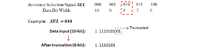
Fig. 7 shows the architecture of the ARSC consists of several parts, including the input buffer, two 2D -DCT blocks ( is 8 here), logic control unit, an accuracy selection signal and an output buffer. Since SC still has longer computing latency compared to the conventional arithmetic units, we propose to use the parallel computing structure to accelerate the process. The input buffer will send 8 image pixel data to the 2D DCT block once due to the 8-DCT method. The frameworks of the DCT and the inverse DCT block actually are the same. The 2D DCT block is made up with two ARSC MAC units for the 1D DCT process, and an intermediate buffer. The intermediate buffer is used to save the output data from the 1D DCT process as the first ARSC MAC unit get the data from input in row and the second one in column, respectively. The second ARSC MAC unit will not start working until the intermediate data buffer is full. And the Logic Control Unit will send the control signal to all of the blocks to control the data flow of the whole DCT/IDCT process.

IV Hardware Implementation
To evaluate the hardware cost of the re-configurable stochastic computing module, including the area, delay and power consumption of the module, the proposed design was implemented in Verilog and synthesized using Xilinx ISE 14.7 for XC6SLX45 device of Spartan-6 family. Different from the ASIC-based module, FPGA mainly use the LUT-based operations [18]. So for the design area measurement, we simply count the number of LUTs after the module is synthesized. As mentioned in Sec. III, the design totally utilizes 17569 LUTs to support the parallel SC blocks. We show the details of the FPGA hardware resource utilization information in table I. To evaluate the power consumption, we use the Xilinx Power Estimator downloaded from the official website, which can easily obtain the total power consumption. We’ll discuss the power consumption of the design later in Sec. V. For the delay measurement, we obtain the critical path of the ARSC design from the Xilinx ISE 14.7 timing summary after the design is synthesized, showing that the hardware delay, which is calculated from the worst case critical path, is 11.348ns. It means that the highest frequency the ARSC design can run is 88.1M. Since we use the digital clock manager (DCM) IP of Xilinx ISE 14.7 to generate the clock signal and the input system clock of the DCM is 100M for the Spartan-6 family boards. The highest frequency DCM can output is 85.7M. So we choose this frequency to be the initial global clock signal of the ARSC design.
| |||||
| Slice Registers | Slice LUTs | LUT FF Pairs | RAMB16BWERS | RAMB8BWERS | |
| 11041 | 17569 | 18098 | 66 | 1 | |
V Experimental results and discussion
In this section, we present results from the proposed ARSC computing method for the aging mitigation. The proposed ARSC DCT/IDCT image compression algorithms were implemented on the Xilinx XC6SLX45 FPGA platform.
We first show the image compression results with different accuracy in Fig. 8. The Fig. 8 shows the original figure without any compression. And Fig. 8 Fig. 8 show the image quality after the DCT/IDCT sequence computing with different accuracy, from 10-bit to 6-bit. We use PSNR (Peak Signal to Noise Ratio) to evaluate the accuracy of the image compressing/decompressing process, which is shown in Table. II.


If we consider the NBTI induced aging process, which causes the chip frequency going down over time due to the increased threshed voltage. To measure the amount of frequency decrease, we use the time dependent degradation aware Nangate 45nm standard cell library from Karlsruhe Institute of Technology (KIT) [4] to calculate the chip frequency after 10 years. We use Synopsys design suite to synthesize the ARSC-based DCT/IDCT design. The timing analysis shows that frequency of the ASIC-based design of DCT/IDCT will decrease from 1205M to 1064M, as shown in Fig. 1. To simulate the aging process by FPGA, we simply adjust the frequency output from the DCM by the same ratio, which is 85.7M to 75.7M (we note that such mapping may not be perfect as the design technologies used in our ASIC and FPGA are different). For the DCT/IDCT process, the aging effect directly affect the throughput. The time of the whole process, including both of the DCT and IDCT process, is used to calculate the throughput.
We show that the throughput with different precision at different clock frequencies in Fig. 9. The x-axis is the bit width we use in the stochastic multiplication when we perform the DCT/IDCT computing. The y-axis is the throughput, meaning the number of images the design can deal with per second. Fig. 9 also shows the throughput of 7.19 images per second for different frequencies and precision with the dashed black line. As we can see, initially (when the aging process hasn’t start yet), if we use the full 10-bit precision, the throughput at 85.7MHz clock frequency is 7.19. When the clock frequency decreases to 43.8MHz, we can still keep the same throughput if we truncate the precision by only one bit (from 10 to 9). Due to the aging process, the throughput will decrease to 6.35. If we degrade the precision by one bit (9-bit), the throughput will increase to 12.42, which obviously, is larger than the initial throughput. The red line of dashes in Fig. 9 shows this very clearly. And, by decreasing the precision of SC multiplication to 6-bit, the throughput will be about 12 times of the 10-bit precision, which shows huge space we can mitigate the aging effects if such accuracy is still accepted in practical applications.
Due to the difficulty of obtaining the hardware delay of the scenarios in which the data bit width is not 10-bit during SC computing process, we use the effective latency to evaluate the timing performance of our design. The effective latency of the ARSC design is actually the inverse of the throughput, since it represents the time interval between the input and the output. We show the latency at the 5th column of Table II.
From Table II, we show that our design can do the dynamic power management by adjusting the working frequency as well. By doing the trade off between the throughput and the accuracy mentioned before, we can keep the throughput by sacrificing accuracy when the frequency is cut down due to some low power consumption requirement situation. For example, if we want to keep the throughput as 7.19 here, when the power goes down, the frequency of the ARSC design will also decrease. Thus, the precision (bit width) of the data our proposed ARSC design can work will also decrease. We show this clearly in Fig. 10. We notice that we can save near 74% of power consumption by sacrificing 10.67dB of the accuracy loss. We also observed that the proposed ARSC computing framework allows much aggressive frequency scaling, which can lead to order of magnitude power savings compared to the traditional dynamic voltage and frequency scaling (DVFS) techniques.
|
Frequency (MHz) | Power (W) | PSNR (dB) | latency (s) | |
|---|---|---|---|---|---|
| 10 | 85.7 | 0.292 | 38.12 | 0.139 | |
| 9 | 43.8 | 0.177 | 34.68 | 0.071 | |
| 8 | 22.9 | 0.120 | 31.27 | 0.037 | |
| 7 | 12.4 | 0.092 | 28.70 | 0.020 | |
| 6 | 7.1 | 0.077 | 27.45 | 0.012 |
VI Conclusion
In this paper, we have proposed a novel accuracy-reconfigurable stochastic computing (ARSC) framework for dynamic reliability and power management. The new ARSC design can dynamically change accuracy via bit-width change of the data. In this way, the new method can accommodate the long-term aging effects by slowing the system clock frequency at the cost of accuracy while maintaining the throughput of the computing. We designed and validated the ARSC-based discrete cosine transformation (DCT) and inverse DCT designs for image compressing/decompressing applications on the Xilinx Spartan-6 family XC6SLX45 platform. Experimental results show that one can easily mitigate the long-term aging effects by accuracy reduction while maintaining the throughput of the whole computing process using simple frequency scaling. In our example, we show that one-bit precision loss for the input data, which translated to 3.44dB of the accuracy loss in term of Peak Signal to Noise Ratio (PSNR) for images, one can sufficiently compensate the NBTI induced aging effects in 10 years while maintaining the pre-aging computing throughput of 7.19 frames per second. At the same time, one can save 74% power consumption by 10.67dB of accuracy loss. The proposed ARSC computing framework allows much aggressive frequency scaling, which can lead to order of magnitude power savings compared to the traditional dynamic voltage and frequency scaling (DVFS) techniques.
References
- [1] A. Alaghi, W. Qian, and J. P. Hayes, “The promise and challenge of stochastic computing,” IEEE Transactions on Computer-Aided Design of Integrated Circuits and Systems, vol. 37, no. 8, pp. 1515–1531, 2018.
- [2] “Failure Mechanisms and Models for Semiconductor Devices.” In JEDEC Publication JEP122-A, Jedec Solid State Technolgy Association, 2002.
- [3] “Critical Reliability Challenges for The International Technology Roadmap for Semiconductors (ITRS),” 2003. In International Sematech Technology Transfer Document 03024377A-TR, 2003.
- [4] “Degradation-aware cell libraries, v1.0.” http://ces.itec.kit.edu/dependable-hardware.php.
- [5] S. X.-D. Tan, H. Amrouch, T. Kim, Z. Sun, C. Cook, and J. Henkel, “Recent advances in EM and BTI induced reliability modeling, analysis and optimization,” Integration, the VLSI Journal, vol. 60, pp. 132–152, Jan. 2018.
- [6] S. X.-D. Tan, M. Tahoori, T. Kim, S. Wang, Z. Sun, and S. Kiamehr, VLSI Systems Long-Term Reliability – Modeling, Simulation and Optimization. Springer Publishing, 2019.
- [7] H. Amrouch, B. Khaleghi, A. Gerstlauer, and J. Henkel, “Towards aging-induced approximations,” in Proceedings of the 54th Annual Design Automation Conference 2017, pp. 1–6, 2017.
- [8] A. Naderi, S. Mannor, M. Sawan, and W. J. Gross, “Delayed stochastic decoding of ldpc codes,” IEEE Transactions on Signal Processing, vol. 59, no. 11, pp. 5617–5626, 2011.
- [9] P. Li, D. J. Lilja, W. Qian, K. Bazargan, and M. D. Riedel, “Computation on stochastic bit streams digital image processing case studies,” IEEE Transactions on Very Large Scale Integration (VLSI) Systems, vol. 22, no. 3, pp. 449–462, 2013.
- [10] K. Kim, J. Kim, J. Yu, J. Seo, J. Lee, and K. Choi, “Dynamic energy-accuracy trade-off using stochastic computing in deep neural networks,” in 2016 53nd ACM/EDAC/IEEE Design Automation Conference (DAC), pp. 1–6, IEEE, 2016.
- [11] H. Sim, D. Nguyen, J. Lee, and K. Choi, “Scalable stochastic-computing accelerator for convolutional neural networks,” in 2017 22nd Asia and South Pacific Design Automation Conference (ASP-DAC), pp. 696–701, IEEE, 2017.
- [12] H. Sim and J. Lee, “A new stochastic computing multiplier with application to deep convolutional neural networks,” in 2017 54th ACM/EDAC/IEEE Design Automation Conference (DAC), pp. 1–6, IEEE, 2017.
- [13] R. Hojabr, K. Givaki, S. Tayaranian, P. Esfahanian, A. Khonsari, D. Rahmati, and M. H. Najafi, “Skippynn: An embedded stochastic-computing accelerator for convolutional neural networks,” in Proceedings of the 56th Annual Design Automation Conference 2019, p. 132, ACM, 2019.
- [14] S. Liu and J. Han, “Energy efficient stochastic computing with sobol sequences,” in Proceedings of the Conference on Design, Automation & Test in Europe, pp. 650–653, European Design and Automation Association, 2017.
- [15] F. Neugebauer, I. Polian, and J. P. Hayes, “Building a better random number generator for stochastic computing,” in 2017 Euromicro Conference on Digital System Design (DSD), pp. 1–8, IEEE, 2017.
- [16] K. Kim, J. Lee, and K. Choi, “An energy-efficient random number generator for stochastic circuits,” in 2016 21st Asia and South Pacific Design Automation Conference (ASP-DAC), pp. 256–261, IEEE, 2016.
- [17] B. R. Gaines, “Stochastic computing systems,” in Advances in information systems science, pp. 37–172, Springer, 1969.
- [18] Y. Guo, H. Sun, and S. Kimura, “Small-area and low-power fpga-based multipliers using approximate elementary modules,” in 2020 25th Asia and South Pacific Design Automation Conference (ASP-DAC), pp. 599–604, IEEE, 2020.