Towards Ultrasensitive SQUIDs Based on Submicrometer-Sized Josephson Junctions
Abstract
We recently demonstrated a 1-order axial gradiometer SQUID system, which is operated in a liquid He dewar with negligible noise contribution. The achieved close to SQUID-limited measured coupled energy sensitivity of corresponds to a white field noise below 180 aT Hz-1/2. In order to further improve the SQUID noise performance, the junction capacitance was reduced by decreasing its lateral size from m to below m. This was realized by extending the fabrication process for submicrometer-sized Josephson Junctions based on the HfTi self-shunted junction technology to an SIS process with AlO as the insulating layer. We achieved energy sensitivities of 4.7 and 20 at 4.2 K for uncoupled and coupled SQUIDs, respectively. We also investigated the temperature dependence of the noise of the uncoupled SQUIDs and reached an energy sensitivity of 0.65 in the white noise regime at 400 mK.
Index Terms:
Noise, sub-m Josephson junctions, SQUID.I Introduction
Superconducting quantum interference devices (SQUIDs) are the most sensitive detector for magnetic flux, and state-of-the-art PTB current sensor SQUIDs reach a coupled energy sensitivity of about 30 when operated at 4.2 K ( is Planck’s constant). For the detection of weak magnetic signals from room temperature samples, e.g., encountered in biomagnetism, SQUIDs are typically coupled to a superconducting pick-up coil and operated in a glass fiber liquid He dewar. In our latest system, the thermal noise from the superinsulation and thermal shields could be avoided enabling a close to SQUID-limited white magnetic field noise below 180 aT Hz-1/2 for a 45 mm diameter gradiometric pick-up coil [1, 2]. Hence, improvements in SQUID performance would not only be beneficial for biomagnetism, but also for other applications where SQUID noise is the limiting factor.
For an uncoupled dc SQUID of inductance , critical current , shunt resistance and junction capacitance , the design parameters and are chosen close to 1 for optimal noise performance. In this case, numerical simulations yield for the energy sensitivity per unit bandwidth , where is the Boltzmann constant and the temperature [3].
The energy sensitivity of the uncoupled SQUID is determined experimentally by , where is the measured flux noise power density. For a SQUID with integrated input coil (current sensor SQUID), the coupled energy sensitivity is referred to the input coil (with inductance ) via the coupling coefficient . Here, is the mutual inductance between the input coil and the SQUID loop. The equivalent field noise can be obtained from , where is the total inductance of the input circuit and the field sensitive area of the pick-up loop.
The aforementioned simulations show that an improvement in the energy resolution is possible by the following:
- 1.
lowering the SQUID inductance by decreasing the size of the SQUID loop;
- 2.
reducing the Josephson junction (JJ) capacitance by decreasing the junction area;
- 3.
cooling down the SQUID device to reduce thermal noise in the shunt resistors.
While approach 1) has been implemented in nano-SQUIDs, it is impractical for current sensor SQUIDs with high inductance pick-up coils (H) as coupling to the small SQUID loop becomes excessively difficult.
Consequently, in this work, we present our development of dc SQUIDs based on submicrometer-sized Josephson Junctions to reduce the JJ capacitance and thereby increase sensitivity. We also present the noise performance for temperatures as low as 400 mK. This is important for applications where the SQUIDs are cooled to below 4.2 K.
II Submicrometer-sized Josephson Junctions
II-A Junction Technology
SQUIDs based on cross-type submicron-sized JJs have been reported in the literature [4, 5]. We chose a fabrication process for the submicrometer-sized JJs based on the established HfTi self-shunted junction technology developed at PTB for JJs arrays [6] and nano-SQUIDs [7]. The technology has been extended to a superconductor-insulator-superconductor (SIS) process utilizing conventional AlO as the insulating layer with a nominal critical current density of 1 kA cm-2. The fabrication is indicated in Fig. 1 and uses electron-beam lithography and a chemical mechanical planarization (CMP).
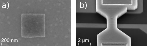
The trilayer JJ is patterned using inductively coupled plasma reactive ion etching (ICP-RIE) for the Nb counter electrode (200 nm) and ion beam etching for the insulating junction layer (20 nm Al + x nm AlO). This is followed by an anodization to electrically isolate the JJ edges and an SEM image of a m2 junction after this step is shown in Fig. 2(a). To pattern the Nb base electrode (160 nm), ICP-RIE is used once more. After depositing the SiO2 insulation between the base and the Nb wiring, superfluous SiO2 is removed via CMP to reveal the junction contacts and for planarization of the wafer surface. For the realization of superconducting connections between the base and wiring electrodes, vias in the insulation are opened by ICP-RIE. Subsequently, patterning of the resistance layer AuPd (75 nm) for the shunt resistors is done with a lift-off process and the final Nb wiring (560 nm) is structured using again ICP-RIE. An SEM image of a m2 AlO junction with the wiring electrode is shown in Fig. 2(b).
II-B Junction Characterization
The - curves of various series junction arrays were measured at 4.2 K. Exemplary data for the m2 JJ array are shown in Fig. 3, and the extracted parameters are listed in Table I. The critical current is significantly reduced compared to the nominal values and the results from the shunted JJs in the miniature SQUIDs (Section III) due to finite temperature and rf interference. The gap voltage is determined at and the subgap resistance at 2 mV. is the normal resistance.
| JJ length | ||||||
|---|---|---|---|---|---|---|
| (m) | (A) | (A) | (mV) | () | (k) | |
| 0.8 | 6.40a | 3.36 | 2.63 | 234 | 4.79 | 20.5 |
| 0.7 | 4.90a | 2.34 | 2.63 | 299 | 6.01 | 20.0 |
| 0.6 | 3.60a | 1.64 | 2.63 | 397 | 9.98 | 25.1 |
-
a nominal values
III SQUIDs based on sub-m-sized JJs
III-A SQUID Parameters
For the evaluation of the Nb-AlO-Nb submicron-junction process, miniature SQUID magnetometers with were fabricated. These have square junctions with side lengths of m and differ in their . The design parameters for K are listed in Table II together with the values for a test SQUID with conventional JJs of 2.5 m size. Current sensor SQUIDs with and m2 JJs were also fabricated and characterized. All submicrometer-sized JJ devices were fabricated on a set of two wafers with nominally identical fabrication parameters.
| # | JJ length | |||||||
|---|---|---|---|---|---|---|---|---|
| (m) | (A) | () | () | () | () | |||
| SQ-1 | 0.8 | 6.4 | 40a | 47 | 1.7 | 0.43 | 4.1b | 1.7 |
| SQ-2 | 0.8 | 6.4 | 40a | 34 | 0.90 | 0.43 | 5.3 | 2.4 |
| 2.5c | 6.55 | 400 | 10 | 0.80 | 0.44 | 27 | 8.0 |
-
a estimated from 400 mK data
b mean value
c equivalent square length of octagonal shaped JJ
The - curve at 4.2 K of miniature SQUID SQ-2 is shown in the inset of Fig. 4. The indentation appearing at corresponding to a Josephson frequency of is caused by a resonance of the interconnection stripline between SQUID and wire bonds. was calculated from the bias current needed for maximum voltage and we obtained a mean (eight devices) of A with a standard deviation of A for a single JJ. The capacitance of the m2-sized JJ was estimated from the - curve behavior of SQ-2 at 400 mK. Here, the measured increased from 6.6 to 7.2 A in good agreement with the theoretical expectation [8] resulting in a noise parameter . In this case, suppression of hysteresis by thermal noise is reduced and needs to be close to one. We estimate leading to for SQ-2. This is also consistent with where is the JJ area. In contrast, SQ-1 showed hysteresis in the - curve at 400 mK.
III-B Performance
We first discuss the performance determined at 4.2 K. The measurements were carried out in a liquid He bath using a direct read-out scheme and a single-stage configuration. The equivalent flux noise due to voltage and current noise of the XXF read-out electronics [9] was subtracted to obtain the intrinsic SQUID flux noise . At 4.2 K our devices fulfill and the theoretical limit can be estimated by
| (1) |
which is valid for an arbitrary value of [3].
As shown in Fig. 4, the intrinsic white energy sensitivity was 4.1 and 5.3 for SQ-1 and SQ-2, respectively. Those values are a factor of more than 5 better compared to our conventional technology with junction sizes of m2, which shows . The slightly larger experimental for SQ-2 is also expected theoretically using (1); however, the absolute values are about a factor of 2 larger. A possible origin might be suboptimal biasing or insufficient subtraction of the electronics contribution at 4.2 K as is reduced in this case. A two-stage read-out scheme should be employed in future studies.
The energy sensitivity increases at lower frequencies with a typical value 37 at 1 Hz corresponding to 900 n Hz-1/2, which was reproducible for the different devices. Interestingly, the low-frequency noise follows a behavior with two distinct -values. For the m-sized JJ SQUID and SQ-1 (chip T3), we find consistent with critical current fluctuations as the origin. In contrast, the remaining SQUIDs show at 4.2 K as has also been observed previously [10, 4].
III-C Temperature Dependence
Measurements below 4.2 K were carried out on a pulse-tube cooler equipped with a 3He sorption unit with the samples mounted in the vacuum space inside an aluminum and lead shield. No special precautions were made to thermally anchor the device to the cold stage of the cryostat. Consequently, the thermal link is mainly provided by the copper wiring used for biasing the SQUID.
Fig. 5 shows the energy sensitivity for temperatures down to 400 mK together with the fitted white noise values (dashed lines) for SQ-2. In agreement with our previous work [10], we observe a reduction in the white noise level , an increase of the low-frequency noise and a shift of the -noise corner to higher frequencies with decreasing temperatures.
In discussing , we refer to Fig. 6, which also contains the 4.2 K-values for all SQ-1 chips. Data for lower temperatures are not included due to the aforementioned hysteresis. At 400 mK, we determine for SQ-2. In addition, the theoretical curve obtained by combining (1) and the temperature dependence , as given in [8] is shown. For K, one finds so that is dominated by the linear -term in (1). For the lower temperatures there is reasonable agreement, whereas at 4.2 K the measured are significantly larger as already mentioned above.
It is worth discussing the temperature dependence of the low-frequency behavior in more detail. The unusual increase with decreasing temperature has been observed before [11] and for 4.2 and 0.4 K the excess noise follows roughly with . However, for the intermediate temperatures of 1 K and 2 K, a low-frequency plateau emerges, which is particularly clear for the 1 K data. Whether this behavior is intrinsic to the fabrication technology remains unclear and requires further studies on a larger number of samples.
III-D Fully Integrated Current Sensor SQUIDs
Based on these results, integrated current sensors were designed and fabricated having a SQUID inductance of 80 pH and m2 JJs. For the input circuit consisting of a 400 nH input coil, a proven double-transformer design was used with a coupling coefficient of [12]. The expected white coupled energy sensitivity of this design is approximately 10 at 4.2 K. In Fig. 7, the results show that we achieve an of 20. The mismatch is most likely due to a parasitic resistance between SQUID and input coil of 75 . The low-frequency noise follows approximately and the set of - curves, given in the inset of Fig. 7, does not show any irregularities, e.g., due to resonances, for SQUID voltages up to V. This could be avoided by the implementation of on-chip rf-filters compared to the miniature magnetometers.
Due to a limited number of fabrication runs the technology has not reached maturity, but the insufficient isolation observed in the current sensor device has been eliminated. Initially, as shown here, a good homogeneity of the JJs critical current could be achieved. However, after extensive alterations in the production technology, the restoration of this condition turns out to be difficult and is an ongoing task.
IV Conclusions
In this work, we presented a proof of concept of a new generation of SQUID sensors based on submicrometer-sized JJs. The fabrication technology was adapted from an established process for SNS junctions and is based on electron-beam lithography and CMP. Small test magnetometer SQUIDs with m2 JJs validated the approach for which we obtained energy sensitivities of about at 4.2 K. When the devices were cooled to 400 mK, we achieved below in reasonable agreement theoretical expectations. A current sensor SQUID utilizing a double transformer scheme suffered from an insufficient isolation and reached of . For a reliable fabrication technology, we expect a performance of at 4.2 K and about when cooled to 400 mK. In order to minimize electronics noise contributions, a two-stage read-out scheme will be employed.
Recent improvements in liquid He glass-fiber dewar construction circumvented the limiting thermal noise contributions, and one can expect a significant impact of such novel devices in biomagnetic measurements. In addition, they will be very useful in fundamental science experiments where SQUIDs are often operated in a superconducting shield environment and cooled down for increased sensitivity.
Acknoledgement
The authors thank M. Petrich, J. Felgner, K. Störr and Th. Weimann for fabrication.
References
- [1] J.-H. Storm, P. Hömmen, D. Drung, and R. Körber, “An ultra-sensitive and wideband magnetometer based on a superconducting quantum interference device,” Appl. Phys. Lett., vol. 110, no. 7, p. 072603, Feb. 2017.
- [2] J.-H. Storm, P. Hömmen, N. Höfner, and R. Körber, “Detection of body noise with an ultra-sensitive SQUID system,” Meas. Sci. Technol., vol. 30, no. 12, p. 125103, sep 2019.
- [3] J. Clarke and A. I. Braginski, The SQUID handbook. Wiley Online Library, 2004, vol. 1.
- [4] M. Schmelz, V. Zakosarenko, T. Schönau, S. Anders, J. Kunert, M. Meyer, H.-G. Meyer, and R. Stolz, “A new family of field-stable and highly sensitive squid current sensors based on sub-micrometer cross-type josephson junctions,” Superconductor Science and Technology, vol. 30, no. 7, p. 074010, 2017.
- [5] J. Luomahaara, M. Kiviranta, L. Gronberg, K. C. J. Zevenhoven, and P. Laine, “Unshielded SQUID sensors for ultra-low-field magnetic resonance imaging,” IEEE Transactions on Applied Superconductivity, vol. 28, no. 4, pp. 1–4, jun 2018.
- [6] D. Hagedorn, O. Kieler, R. Dolata, R. Behr, F. Müller, J. Kohlmann, and J. Niemeyer, “Modified fabrication of planar sub-m superconductor–normal metal–superconductor josephson junctions for use in a josephson arbitrary waveform synthesizer,” Superconductor Science and Technology, vol. 19, no. 4, pp. 294–298, feb 2006.
- [7] S. Bechstein, C. Köhn, D. Drung, J.-H. Storm, O. Kieler, V. Morosh, and T. Schurig, “Investigation of nanoSQUID designs for practical applications,” Superconductor Science and Technology, vol. 30, no. 3, p. 034007, feb 2017.
- [8] V. Ambegaokar and A. Baratoff, “Tunneling between superconductors,” Physical Review Letters, vol. 11, no. 2, pp. 104–104, jul 1963.
- [9] “XXF-1 Electronics, Magnicon GbR, Barkhausenweg 11, 22339 Hamburg, Germany; Available: http://www.magnicon.com,” See http://www.magnicon.com/squid-electronics/ for description of electronics and data sheets.
- [10] D. Drung, J. Beyer, J.-H. Storm, M. Peters, and T. Schurig, “Investigation of low-frequency excess flux noise in dc squids at mk temperatures,” Applied Superconductivity, IEEE Transactions on, vol. 21, no. 3, pp. 340–344, Jun. 2011.
- [11] F. C. Wellstood, C. Urbina, and J. Clarke, “Low-frequency noise in dc superconducting quantum interference devices below 1 K,” Applied Physics Letters, vol. 50, no. 12, pp. 772–774, mar 1987.
- [12] D. Drung, C. Assmann, J. Beyer, A. Kirste, M. Peters, F. Ruede, and T. Schurig, “Highly sensitive and easy-to-use SQUID sensors,” Applied Superconductivity, IEEE Transactions on, vol. 17, no. 2, pp. 699–704, Jun. 2007.