Numerical study of track distortion in the Large Prototype TPC with end-plate based on bulk Micromegas
Abstract
The present activities for the International Large Detector Time Projection Chamber (ILD-TPC) concern the adoption of the micro pattern devices for the gaseous amplification stage. Seven Micromegas modules which are commissioned on the end-plate of a Large Prototype TPC (LPTPC) at DESY, were tested with a 5 GeV electron beam, under a 1 T magnetic field. During experiments, reduced signal sensitivity as well as distortion in the reconstructed track was observed at the boundaries of these modules. Electrostatic field inhomogeneity near the module boundaries was considered to be the possible major reason behind these observations. In the present work, this hypothesis has been explored using the Garfield simulation framework. It has been possible to contain the computational complexity of the problem with suitable simplifications. Qualitative and quantitative agreements with experimental results have been achieved. Possibility of mitigating the problems has been proposed using the same simulation framework.
1 Introduction
At the International Linear Collider (ILC) [1], the electron-positron beam will collide at in the center-of-mass frame. A possible option of upgrading it to higher energies is also being considered. The golden channel at gives the unique opportunity of detecting Higgs events even without looking at its decay[2]. Higgs mass can be determined with excellent precision from the measurement of Z boson, decaying in leptons. The physics studies aimed at the ILC have pushed the requirements for its detectors to an unprecedented level. These requirements include excellent momentum resolution and good particle identification [3]. The International Large Detector (ILD) [3] is one of the two detector concepts for the ILC. A Time Projection Chamber (TPC) [4, 5] (Fig. 1) has been foreseen as the central tracker of the ILD and is likely to be installed just around the vertex detectors to accomplish continuous tracking with high efficiency.

The size of the planned ILD-TPC is for inner radius, for outer radius, and (divides two parts) in z direction [3]. The TPC is expected to be placed inside a magnetic field of . Under these conditions, the ILD-TPC is projected to have the spatial resolution of less than and 2-hit resolution of less than [3]. The Linear Collider TPC (LCTPC) collaboration [6] was formed to pursue the the design, development and test of a Large Prototype TPC (LPTPC) [7, 8].
The Micro-Pattern Gaseous Detectors (MPGDs) [9], due to their wide variety of geometries and flexible operating parameters, become a common choice for tracking and triggering detectors. The LCTPC collaboration has, therefore, investigated the use of MPGDs for the TPC readout[10]. One of the main advantage of the MPGD-based redaout over the conventional wire-based amplification system is the fact that in the amplification region, effects are small and do not affect the resolution.
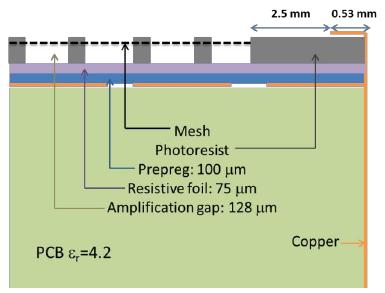
One of the most widely used MPGDs is Micro-MEsh Gaseous Structure (Micromegas) Detectors, invented by Y. Giomataris et al. [11]. Up to seven resistive Micromegas (MM) [12] modules have been studied at the LPTPC end-plate since 2009 through 2015 and they have shown promising performance as required for the ILD-TPC [13, 14]. The keystone-shaped modules have identical size of so as to fit in the end-plate. The amplification gap and the micro-mesh wire pitch have been chosen to be and , respectively. Different types of resistive layers with surface resistance around have been tested at the LPTPC with an electron beam of energy ranging from , under a magnetic field of . The anode readout of a Micromegas module is segmented in 1726 pads of size and arranged in 24 rows. The pads are readout with the AFTER-based electronics designed for the T2K experiment [15]. A thin copper frame that is connected to the resistive layer of the layout, is kept at ground potential. The reconstruction of a typical track on the TPC end-plate, consisting of seven modules, is shown in Fig. 2. The close-up schematic diagram of the region near the module edge is shown in Fig. 2 [16].



During the analysis process, a reduced signal sensitivity was observed near the edge of the module. It was also found that the spatial resolutions of all the pads were consistent, except for those near the module edge. Figure 3 shows the distortion (residual) plot versus the row radius without or with magnetic field [17]. Residual of the pad hits on the extreme rows of the MM modules have larger magnitude with respect to the other rows. The transfer between two detector modules is seen and, in-between them, the distortion is larger and leads to ‘S’ like shape as shown in Fig. 3 and Fig. 3. It should be noted that the difference between the distortions is expected since in the presence of magnetic field, the transverse diffusion is known to be reduced and the distortion is likely to be influenced by effect. The most likely reason leading to this distortion is the electric field inhomogeneity introduced by the gap between a module and its neighbor. Similar conclusion was obtained by studying the electric field configuration near the module boundaries with GEM amplification stages using a simplified version of the actual experimental setup [18, 19]. In what follows, besides investigating the electric field at the module boundaries for an end-plate having Micromegas modules, we have numerically estimated the residuals for a more realistic geometry and compared our estimates with the experimental data.
2 Numerical approach
2.1 Simulation Tools
Garfield [20, 21] simulation framework has been used in the following work. The 3D electrostatic field simulation has been carried out using neBEM [22, 23, 24] toolkit. Besides neBEM, HEED [25, 26] has been used for primary ionization calculation and Magboltz [27, 28] for computing drift, diffusion, Townsend and attachment coefficients.
2.2 Optimization of numerical model
Instead of considering all seven Micromegas modules for simulation, an attempt has been made to optimize computational expenses in terms of both number and size of the modules in the numerical model. The aim has been to minimize computation retaining the essential physics issues in the solution. The cross-sectional view of the simulated geometry is shown in Fig. 4 where different parts of the geometry are explained.

For this part of the work, two Micromegas modules of size have been placed side by side, as shown in Fig. 5 and we have focused our attention on the variation of potential and electric field close to the vicinity of the gap between the two modules. Similarly, since the track distortion studies carried out in this work involves the effect of the inter-modular space on track reconstruction, only three modules have been considered as shown in Fig. 5. This configuration allows two inter-modular gaps to appear in the model which is also typical in the experimental scenario (Fig. 3). It may also be mentioned here that while the gap between any two modules is , the grounded copper extends to and the photoresist is wide, as shown in Figs. 2 and 5. Please note that the mesh begins at a distance of from the mid-point between two modules. Finally, it should be noted that for the 2-module geometry, is the mid-point between the two modules, while for the 3-module geometry, and are the two mid-points among the three modules along y.


Two different tools which rely on completely different mathematical foundations have been compared to ensure the rationality of the numerical estimates. The Finite Element Method (FEM) based commercial solver COMSOL Multiphysics [29] and the neBEM + Garfield combinations have been used for this purpose. It should be mentioned here that the geometry of the overall device poses an extremely difficult problem for the both solvers. The component lengths span over several orders of magnitude. For example, length of a module is whereas the copper frame width is (7000:1). The situation is even worse if the entire device is considered. Despite the difficulties, an effort was made to maintain accuracy of the results and in Figs. 6, 6, 7 and 7, comparison between the two electric field solvers have been presented. Despite the difference in mathematical models and numerical implementation of the solution procedure, the estimates agree with each other in all broad aspects. Away from the gap, the field values are found to be uniformly distributed but near the gap the transverse electric field is sharply increasing from (nominal value) to , while the axial field is found to rise from the nominal value of around to . Noticeable non-uniformity of the electric field along y of the geometry is found to be extended up to nearly from the centre of the gap, i.e. within the region where the micro-mesh is known to exist. Beyond this region of non-uniformity, all the fields are found to attain and maintain their nominal values.
There are differences in magnitudes between the electric fields estimated by different approaches. The maximum disagreement is approximately 20% in the most severe case, as shown in Fig. 6, but all the characteristic features are found to be repeated using both the approaches. From this study, we conclude that the electric field estimated by the Garfield + neBEM combination are accurate and use this framework for further studies.
According to the present understanding, the distortion is driven by the non-uniformity of the electrostatic field at the module boundaries. Thus, the reduction in size has been pursued as long as the features of the electrostatic field at the edges remain unaltered from larger modules. As far as electrostatic non-uniformity is concerned, the geometry with the chosen smaller modules is expected to be representative of the real end-plate used in the test beams. A brief numerical experiment has been performed to decide the optimum size of the module in the numerical model, as described below. For this part of the work, we have considered four possible sizes of MM modules which as shown in Table 1.
| Geometry | Size |
|---|---|
| S1 | |
| S2 | |
| S3 | |
| S4 |
We present the effect of module size on the field near the module boundary. In Figs. 8 and 9, estimates have been compared close to the module boundary (the zero value coincides with the mid-point between the two modules) at above the anode plane (which is equivalent to a micron above the top-most surface of a given module) and above the anode plane. It can be seen that the estimated field values are identical for all the four sizes of the numerical modules. Similarly, values have been compared in Figs. 8 and 9. While Fig. 8 shows excellent agreement among the different sizes, Fig. 9 indicates that for the smallest numerical model is different from bigger three sizes. From this study, we conclude that except the smallest numerical model, the other three models produce estimates of electric fields that are consistent with each other. In order to reduce computational expenses, the smallest one among the allowed three, the model, is chosen for further studies.
Although the modelled geometry used in the present calculations is smaller and simpler than that of the real Micromegas on the LPTPC end-plate in terms of size and number, all critical parameters (e.g., the thickness of the copper frame and the photoresist wall, gap between the modules) which influence the electric field near the gap are given realistic values. By comparing the experimental condition, as depicted in Fig. 2, and the numerical model shown in Fig. 5 and Fig. 4, the following may be pointed out:
- •
The actual experiment was performed using a resistive bulk Micromegas, whereas, for this simulation, the standard bulk Micromegas has been considered.
- •
Instead of mesh, zero-thickness plane has been used to model the micro-mesh plane.
- •
A continuous grounded anode plane has been placed below the mesh plane.
- •
To maintain a uniform drift field, the drift plane has been placed above the modules.
- •
As in the experiment, thick photoresist has been used to support the modules.
- •
True to the experiment, a copper layer has been connected all around the module to the ground.
- •
Between the modules there is a gap of which follows the experimental situation.
It should also be mentioned that, for the results presented here, the micro-mesh plane has been biased with a potential of whereas has been applied to the drift plane, thus creating a drift field of . In all the cases, true to the experiment, a magnetic field of either or has been applied. For the remaining calculations presented below, gas ( , , ) has been considered. The track along which the calculations have been performed are shown in Fig. 5. It should be mentioned here that while -- coordinate system has been used in the experimental data interpretation, the numerical model utilizes the Cartesian -- coordinate system. The - in experiment corresponds to x in numerical model and, similarly, in experiment corresponds to y in simulation.
3 Results


3.1 Drift Lines
To study the effects of the field, a large number of electrons are released from the track as shown in Fig. 5 at a distance of above the module. These electrons drift towards the readout plane (Fig. 10). Near the edge of the module, the drift lines get distorted significantly. It is observed from Fig. 10 that of electrons are lost on the additional ground and the photoresist. From the drift lines, it is also clear that the number of electrons at the readout pads close to the module edge is much less in comparison to that at the central part of the module. The presence of the magnetic field reduces the diffusion as shown in Fig. 10, as expected, but at the same time it introduces movement along y (for this particular configuration). This is natural since, under the application of magnetic field, the force comes into play and modifies the drift lines. A view from the top, shown in Figs. 10 and 10 complements the elevation projections presented in Figs. 10 and 10. From these two views it is clear that the electrons have an inclination to drift towards the photoresist support or the nearby ground plane. It may also be noted that, for the magnetic field, the effect of diffusion is less and track distortion is restricted to a smaller fraction of the considered track. Although Fig. 10 present the situation corresponding to a given number of events along few tracks (10 tracks, 80 equidistant electrons per track) of what is clearly a statistical process, the indications are reasonably clear.
From the drift lines shown above, it is clear that a loss of efficiency will occur for pads close to the module edges. In order to assess the loss, the y axis has has been divided into bins and the number of electrons within each bin has been counted. The variation of the count along the track has been presented in Fig. 11. The loss of efficiency, close to the edge is higher for (loss of more than up to from the module edge) than that of (loss of more than up to from the module edge).
3.2 Residual calculation
In the experiment, the track is reconstructed out of the measured hit positions. The residual of a pad hit is given by:
| (3.1) |
where, is the true position of the hit and is the estimated hit position based on the track fitting with the rest of the points. The residuals provide an estimate of the distortion introduced during track reconstruction. In the simulation, as the track (i.e. the starting coordinates of the electrons) is well defined, we can simplify the residual calculation without track fitting. The ending coordinates of the electrons (i.e. the final pad hit point) are obtained from Garfield. The residuals of the hits on the anode plane are estimated by taking the difference between the respective start and end coordinates of the electrons. They are then averaged over the number of events (tracks).
From the residual histograms (Fig. 12), it can be observed that residual along x reduce significantly in the middle of the module due to the presence of a magnetic field. This is easily explained by noting that magnetic field decreases diffusion since it acts as an additional constraint that makes the charged particle follow electric field lines. The same trend is observed in the residual along y. The x-residual plots without the magnetic field (Fig. 13) does not show any distortion in the middle of the modules. The shift between the modules is clearly visible. When a magnetic field is applied, the magnetic field together with the transverse components of the electric field gives rise to the Lorentz force near the gap (Fig. 10). This force leads to a distortion along x and as a result, the magnitude of the residuals are high near the module gaps, as shown in Fig. 13.
The y-residual plots without the magnetic field shows a large distortion near the edge due to the electrical field inhomogeneity. In presence of the magnetic field, the lower diffusion helps to reduce the the residual value (Figs. 12 and 13).
Although the numerical model is simpler and smaller than the real detector, we have compared the numerical estimates against the experimentally measured values, as shown in fig. 3. The length of the numerical module is only , in comparison to of the real module. As a result, the y-range in the numerical estimate () is much smaller in comparison to the experimental one (). By comparing Figs. 3 and 13, it is observed that for the case, distortion in both the cases are found to be around , while for the case, the distortions are around . Thus, despite the use of a smaller and simpler model for the numerical simulation, the estimates are qualitatively and quantitatively comparable to the experimental results. It may be safely concluded that the numerical model represents the experimental scenario reasonably well and may be used for further studies on possible design modifications. The x and y spatial resolutions are plotted in Fig. 14. Spatial resolution is worsened near the edges. In presence of the magnetic field, the resolution improves.
3.3 Possible design modification
Since the electrostatic field inhomogeneity has been identified as the principal deciding factor determining the distortion during track reconstruction in a multi-module TPC, the obvious approach to reduce the distortion is to try and modify the electrostatic field configuration near the module edges. The main difference between the proposed configurations and the original one is the attempt to maintain the copper frame and micro-mesh at the same potential so that the possibility of generating a transverse electric field is minimized. Since the anode and the copper frame no longer has the same potential, they are no longer continuous and a photoresist separates the two to ensure electrical insulation (Fig. 15). Different possible configurations which have been considered, are listed in table 2.

| Case | Description | Mesh | Copper Frame | Anode |
| Voltage | Voltage | Voltage | ||
| Case 1 | Anode and copper | -380 V | 0 V | 0 V |
| frame in contact | ||||
| Case 2 | Photoresist between | -380 V | 0 V | 0 V |
| Case 3 | anode and copper | 0 V | 0 V | 380 V |
| Case 4 | frame | -380 V | -380 V | 0 V |
From Figs. 16, 16, 16 and 16, it is observed that introduction of the additional photoresist block used to separate anode and the copper frame does not introduce significant difference in the field configuration. The effect on the computed residual, as shown in Fig. 17 is, as a result, negligible. On the other hand, as shown in Fig. 18, both the transverse and vertical fields are significantly altered from the original configuration when Case 3 and Case 4 are considered. The magnitudes of distortions are reduced to approximately of their earlier values. The two cases where the mesh and copper frame and supports are at the same voltages, the field configurations are naturally the same. This fact is observed also the pattern of the residuals as shown in Fig. 19 in which, just as in the case of field configuration, the magnitude of the residuals are reduced by more than of their original values.
The variation of the count along the track has been presented in Fig. 20. In the two cases where the mesh and copper frame and supports are at the same voltages, more number of electrons are focused towards the readout plane. As a result, collection of electrons at the first pad increases improving from close to 0 to almost of the maximum possible count of 600. The spatial resolution near the edges improves as shown in Fig. 21.
4 Conclusion
Following the experimental activities and related data analysis, we have investigated the origin of the track distortions observed close to the module edges. We have been able to numerically simulate the observed patterns successfully, and achieved quantitative agreement with the experimental data. This is despite the fact that the entire simulation is done with a number of simplifications in the geometry of the detectors. The intrinsic parameters, like amplification gap, thickness of the photoresist and the ground frame, the inter-modular distances and the TPC gas are maintained true to the experimental values for this calculation. The miniaturization of the detector modules in dimensions are made only to avoid computational delay and complexities.
Our computations indicate that the inhomogeneity of the electric field close to the module edges leads to a loss of efficiency of few pads close to the edge. This inhomogeneity also leads to the distortion in residual as observed in the experimental data and degradation of spatial resolution near the module edges. The presence of magnetic field complicates the matter through the effect, since the two fields are no more parallel (due to the fact that the -field is non-uniform). Interestingly enough, the effect of magnetic field is to improve the different figures of merit such as efficiency and resolution. The nature and the magnitude of the distortion closely match the results as seen in the Micromegas based LPTPC. The obtained agreements encourage us to continue with the study and, if possible, propose module design modifications that can alleviate the problem. Several such modification has been discussed in some details. It has been shown that it is possible to reduce the effects of distortion by maintaining the potential of the copper frame at a value similar to that of the micro-mesh.
This work can be considered as the initial step towards design optimization of these complex devices. As a result, it opens up several areas of exploration which need to be investigated in future studies. For example, variation of the shape and dimension of cover electrodes and copper frame need to be pursued in order to optimize the device geometry. Moreover, there are effects of important physical processes such as charging up and finite resistivity that have been ignored in this work. Inclusion of these processes will not only be challenging computationally, but will also enrich our understanding of related device physics.
Acknowledgments
This work has partly been performed in the framework of the RD51 Collaboration. We happily acknowledge the help and suggestions of the member of the RD51 Collaboration. We thank our collaborators from LCTPC collaboration for their help and suggestions. We are thankful to our respective Institutions for providing us with the necessary facilities and IFCPAR/ CEFIPRA (Project No. 4304-1) for partial financial support. Finally, we thank the reviewer for helping us to improve the quality of the manuscript significantly.
References
- [1] T. Behnke (ed.) et al., International Linear Collider Technical Design Report: Executive Summary vol. 1 (2013).
- [2] Keisuke Fujii et al., Physics Case for the 250 GeV Stage of the International Linear Collider arXiv:1710.07621v4 (2018).
- [3] T. Behnke (ed.) et al., International Linear Collider Technical Design Report: Detectors vol. 4 (2013).
- [4] D. R. Nygren et al., Time Projection Chamber, Physics Today vol. 31 (1978) pg 46.
- [5] H.J.Hilke, Time Projection Chamber, Report on Progress of Physics, vol. 73 (2010) pg 36.
- [6] LCTPC Collaboration, Homepage of the LCTPC collaboration, http://www.lctpc.org.
- [7] T. Behnke et al., A Lightweight Field Cage for a Large TPC Prototype for the ILC, Jour. Instrum., vol. 5 (2010) pg P10011.
- [8] P. Schade, Development and construction of a large TPC prototype for the ILC and study of polarisation in decays with the ILD detector, Ph. D Thesis, , (2009).
- [9] M. Hoch, Trends and new developments in gaseous detectors, Nucl. Instrum. Method A vol. 535 (2004) pg 1.
- [10] R. Diener on behalf of the LCTPC collaboration, Development of a TPC for an ILC Detector, Physics Procedia vol. 37 (2012) pg 456.
- [11] Y. Giomataris et al., Micromegas: a high-granularity position-sensitive gaseous detector for high particle-flux environments, Nucl. Instrum. Meth. A, vol. 29 (1996) pg 376.
- [12] M. Dixit el., Position sensing from charge dispersion in micro-pattern gas detectors with a resistive anode, Nucl. Instrum. Meth. A vol. 518 (2004) pg 721.
- [13] P. Schade et al., A large TPC prototype for a linear collider detector, Nucl. Instrum. Meth. A vol. 628 (2011) pg 128.
- [14] D. Atti, Beam tests of Micromegas LC-TPC large prototype, Jour. Instrum., vol. 6 (2011) pg C01007.
- [15] P. Baron et al., AFTER, an ASIC for the Readout of the Large T2K Time Projection Chambers, IEEE Trans. Nucl. Sci. vol. 55 (2008) pg 1744.
- [16] W. Wang, A large area Micromegas TPC for tracking at the ILC, Ph. D Thesis, Univ. of Paris-Sud, (2013).
- [17] D. S. Bhattacharya et al., Test of Micro-pattern Gaseous Detector modules with a large prototype Time Projection Chamber, Proc. Science (EPS-HEP2015) vol. 277 (2015).
- [18] T. Behnke et al., GEM module design for the ILD TPC, Jour. Instrm. vol. 8 (2013) pg C10010.
- [19] K. Zenker, Studies of field distortions in a Time Projection Chamber for the International Linear Collider, Ph.D. thesis, University of Hamburg, DESY (2014).
- [20] R. Veenhof, Garfield-Simulation of gaseous detectors, online at http://cern.ch/garfield.
- [21] R. Veenhof, Garfield, recent developments, Nucl. Instr. and Meth. A vol. 419 (1998) pg 726.
- [22] S. Mukhopadhyay et al., A nearly exact Boundary Element Method, online at http://cern.ch/neBEM
- [23] N. Majumdar et al., Simulation of three dimensional electrostatic field configuration in wire chambers: A novel approach, Nucl. Instr. and Meth. A vol. 566 (2006) pg 489.
- [24] S. Mukhopadhyay et al., Computation of 3D MEMS electrostatics using a nearly exact BEM solver, Eng. Anal. Boundary Elem. vol. 30 (2006) pg 687.
- [25] I. Smirnov, Interactions of particles with gases, online at http://cern.ch/heed.
- [26] I.B. Smirnov, Modeling of ionization produced by fast charged particles in gas, Nucl. Instr. Meth. A vol. 554 (2005) pg 474.
- [27] S. Biagi, Magboltz - Transport of electrons in gas mixture online at http://cern.ch/magboltz.
- [28] S.F. Biagi, Monte Carlo simulation of electron drift and diffusion in counting gases under the influence of electric and magnetic field, Nucl. Instr. Meth. A vol. 421 (1999) pg 234.
- [29] http://www.comsol.com