Imaging Metasurfaces based on Graphene-Loaded Slot Antennas
Abstract
Spectral imagers, the classic example being the color camera, are ubiquitous in everyday life. However, most such imagers rely on filter arrays that absorb light outside each spectral channel, yielding efficiency for an -channel imager. This is especially undesirable in thermal infrared (IR) wavelengths, where sensor detectivities are low, as well as in highly compact systems with small entrance pupils. Diffractive optics or interferometers can enable efficient spectral imagers, but such systems are too bulky for certain applications. We propose an efficient and compact thermal infrared spectral imager comprising a metasurface composed of sub-wavelength-spaced, differently-tuned slot antennas coupled to photosensitive elements. Here, we demonstrate this idea using graphene, which features a photoresponse up to thermal IR wavelengths. The combined antenna resonances yield broadband absorption in the graphene exceeding the efficiency limit. We establish a circuit model for the antennas’ optical properties and demonstrate consistency with full-wave simulations. We also theoretically demonstrate broadband free space-to-graphene coupling efficiency for a six-spectral-channel metasurface. This research paves the way towards compact CMOS-integrable thermal IR spectral imagers.
keywords
Graphene, Infrared, Optical Antenna, Thermal Imaging, Multispectral Imaging, Plasmonics
0.0.1
We take spectral imaging for granted in daily life. Our eyes are spectral imagers, providing information about the composition of what we see. The infrared electromagnetic band covers many chemical absorption resonances and thus also reveals compositional information. In particular, infrared spectral imaging is applied in areas such as gas emission monitoringTratt et al. 2016; Sabbah et al. 2012; Marinelli et al. 1999; Gagnon et al. 2016; Farley et al. 2007; Van Der Meer et al. 2002; Williams et al. 2005, ecological monitoringBen-Dor et al. 2009; Mozgeris et al. 2016; van Aardt and Wynne 2007, food quality controlSingh et al. 2010; Gowen et al. 2007; Cogdill et al. 2004, waste sortingKaraca et al. 2013, biological researchLee et al. 2014 and oceanographyIannarilli et al. 2000.
Spectral imaging aims to measure a “data cube” representing light intensity over two spatial dimensions and and one spectral dimension with channels. Scanning spectral imagers sequentially measure different portions of the data cube over multiple exposures to form the full data cube. A common example is the pushbroom scanner which measures data cube slices while scanning and is thus typically associated with satellites and conveyor belts where either the camera or subject is gradually moving in one directionStuffler et al. 2009; Tratt et al. 2016; Gowen et al. 2007; Karaca et al. 2013. The spectral axis may also be scanned such as in tunable filter-based imagers Marinelli et al. 1999; Slawson et al. 1999, which feature at most light utilization efficiency, or Fourier transform interferometer-based imagers which are bulky and have moving partsSabbah et al. 2012. In contrast, snapshot spectral imagers (SSIs) capture a data cube with a single exposureHagen and Kudenov 2013. This may be achieved using a color filter array similar to that of a color camera, thus limiting efficiency to Fleischman et al. 2019; Park and Crozier 2013; Hagen and Kudenov 2013. Another category of SSIs uses dichroic or dispersive optics to break up incoming light by wavelength before arriving on a focal plane array (FPA). There are many variations of this approachBodkin et al. 2012; Wagadarikar et al. 2008; Pawlowski et al. 2019; Gorman et al. 2010; Lee et al. 2014, but they all require increasing the etendue of the incoming light beam by a factor of , leading to an unfavorable tradeoff between total FPA area, input acceptance angle and spectral resolutionHagen and Kudenov 2013.
Compared to these technologies, the category of imagers based on inherently multispectral pixels is less explored. One such example is the Foveon RGB sensor, which extracts three different electrical signals from different depths in the optically active silicon region, as shorter wavelengths are absorbed closer to the sensor surfaceMerrill 1999. Another approach uses nanoantennas, optical resonators of subwavelength dimensions which nevertheless feature absorption cross sections of order if the antenna is conjugate impedance matched with its load; or, equivalently, if the antenna is critically coupled to the vacuum. Here, we propose a thermal IR multispectral imager where differently sized metallic slot antennas with infrared-sensitive loads targeting spectral channels are tiled to form a metasurface featuring efficient free space-to-load optical energy transfer. Figure 1a shows such a metasurface for . We model graphene as the photosensitive load because its broadband absorption in the mid-IRFalkovsky 2008 and processing flexibilityGoossens et al. 2017; Zanjani et al. 2017 make it suitable for this platform. Not only do the antennas sort incident light by spectral channel, but they also enhance the absorption of the graphene load, bridging the gap between the impedance of free space and graphene, which, when undoped, has an optical sheet resistance no lower than .Falkovsky 2008. Figure 1b shows in detail a single such antenna-coupled graphene photodetector. This detector is designed for a strong photothermoelectric response, in which absorbed light heats up the electron gas in the graphene, resulting in an electromotive force due to the Seebeck effect. The graphene channel is assumed to be isolated from the metasurface by a several-nanometer layer of dielectric, thin enough to not impact the optical properties of the system. The asymmetric position of the graphene channel with respect to the slot allows half of the graphene channel to be gated by metal underneath, yielding the asymmetric graphene Fermi level profile needed for a nonzero net photoresponseGabor et al. 2011; Song et al. 2011. Note that while perfect absorption in this wavelength range has been demonstrated in heavily doped graphene accompanied with metal nanostructuresKim et al. 2018, we limit our consideration to undoped graphene as the peak Seebeck coefficient occurs at very low doping levelsGabor et al. 2011.
For optical absorption, slot antennas offer a few advantages over planar designs such as dipole or bowtie antennas. They have unidirectional radiation patterns, and thus an array of them can perfectly absorb an incident beam, whereas planar antennas require a quarter-wave back-reflector to do so Alaee et al. 2017; Eggleston et al. 2018. The wavelength dependence of the back-reflector phase complicates design of broadband absorbing metasurfaces and exacerbates undesirable antenna-antenna coupling. Additionally, since planar antennas must be supported by transparent dielectric, they cannot be embedded in a CMOS process as the inter-layer dielectric strongly absorbs thermal infrared radiationKischkat et al. 2012; Lin 2007, whereas for slot antennas the dielectric on top and in the perforations may be etched away without sacrificing the mechanical integrity of the antenna.
0.0.2 Results and Discussion
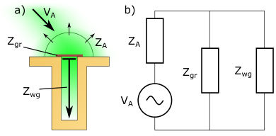
We model the slot antenna depicted in Figure 2a as an aperture antenna fed by a rectangular waveguide terminated in a short circuit a distance behind the aperture. We represent the graphene sheet as a shunt impedance connected in parallel with the waveguide stub. Figure 2b illustrates this circuit with a Thévenin equivalent radiation impedance and source representing the aperture antennaStutzman and Thiele 2013. The rectangular waveguide stub presents an impedance
| (1) |
where and are the characteristic impedance and effective index of the mode of the slot and is the vacuum wavenumber. is the Fresnel reflection coefficient between vacuum and metal for an s-polarized plane wave at an incident angle of , which describes the mode.
The graphene presents a mostly resistive impedance of
| (2) |
using power/current impedance normalizationSchelkunoff 1944. and are defined in Figure 1b and is the sheet conductance of the graphene, modeled here as intrinsic. We calculate using finite element simulations for various and ; we provide more details on these calculations in the Methods section. See Supplementary Figure 1 for an example of the frequency dependence of the impedances in the circuit.
Define as the fraction of available power from Thévenin source , that is dissipated in . Solving the above circuit, we arrive at
| (3) |
where represents reciprocal addition. Define as the partial absorption cross section of light of intensity coupled into the graphene and as the power absorbed in the graphene. For a lossless, conjugate matched antenna, antenna theory predicts where is the antenna’s directivity at the given incident angle and polarizationStutzman and Thiele 2013, which we calculate using finite element simulations. here is the polar angle and is the azimuthal angle. We omit the polarization angle in our notation, implicitly setting it to maximize . Additional ohmic losses and impedance mismatch then reduce the actual absorption cross-section into graphene by a factor , i.e.
| (4) |
We obtain from FDTD simulations of plane waves incident on the graphene-loaded antennas, which we then use to calculate via Equation 4.
Fig. 3 compares between the model described by Equation 3 and FDTD results for antennas of various dimensions. The data show that the model is accurate to within 10% of the peak amplitude and 2% of the resonance wavenumber. We attribute these discrepancies to aspects not captured by the quasi-analytical model, such as our assumption of a perfectly conducting outer antenna face and finite meshing. Despite these shortcomings, the present model allows us to predict slot antenna absorption properties to tolerances comparable to the uncertainty due to variations in metal quality.
To further validate our model, we artificially scale the sheet conductance of the graphene load by factors ranging from to and compare the resulting between the model and FDTD for a single such antenna. The results, shown in Figure 4, show that our model accurately predicts the sublinear scaling of with respect to the load conductivity, with the peak amplitude reaching for a load conductivity of .
Having modeled the individual components, we now discuss broadband absorbing metasurfaces incorporating differently tuned antennas tiled in a periodic array. We use a three-step process to design such metasurfaces. We first constrain and to be the same for all antennas in the metasurface, and choose their values to yield high peak for antennas resonant in the targeted wavelength range. Secondly, we choose the values of for the antennas, following the heuristic that at the wavelength where one antenna’s falls to half its peak amplitude, the next antenna’s should have risen to half its peak amplitude. Finally, we choose the arrangement and pitch of the antennas to be as closely packed as possible while satisfying qualitative fabricability constraints. We also avoid juxtaposing antennas of adjacent wavelength channels to minimize antenna-antenna crosstalk.
The antenna pitch, more accurately described by the Bravais lattice vectors of the array, is a critical parameter in determining the potential absorption efficiency of the array. Light incident from a given direction can only be scattered by the two-dimensional diffraction orders of the lattice. The array can only perfectly absorb an incoming light beam if no nonzero diffraction orders fall within the light cone, barring the event that all higher diffraction orders overlap with nodes in the individual unit cell radiation pattern. By “light cone”, we refer here to the region in the Fourier transform space of the –plane for which radiation can occur, namely . For a square lattice, if the lattice pitch , no higher diffraction orders are within the light cone for any incident angle. In practice, the limited numerical aperture of imaging systems relaxes this constraint.
Targeting the wavelength range, we follow the above methodology and arrive at an array of six antennas with , , and , uniformly spaced and tiled as shown in Figure 1a with a by unit cell. Figure 5 shows the absorption efficiency of normally incident light into the graphene load of each antenna as well as their sum, simulated with FDTD. With an average efficiency of across the to band, this structure improves upon the limit of filter array-based imagers by roughly a factor of two. Note that the unit cell highlighted in Figure 1a is not the primitive unit cell of the lattice, although it was used as the FDTD simulation region due to software constraints.
To further understand the physics of these metasurfaces, we vary the pitch of the unit cell while keeping all other parameters constant. The resulting total absorption efficiency spectra for six different cases are shown in Figure 6a, and their mean efficiencies averaged between and are plotted in Figure 6b. We show the individual absorption contributions from each antenna for each metasurface pitch in Supplementary Figure 2, and we list the unit cell widths and heights in Figure 6c. The data show that the absorption efficiencies are roughly constant, and comparable with the peak efficiencies obtained in Figure 3, up to the –wide unit cell. For larger unit cells, the mean efficiency decreases with increasing unit cell size. This can be understood by analyzing the diffraction characteristics of the various metasurfaces. Sparser metasurfaces have tighter reciprocal lattices and thus more diffraction orders are available within the light cone. For normally incident illumination as we are using here, the minimum wavelength for which no higher-order diffraction occurs (i.e., completely specular reflection) is given by , where and are the unit cell dimensions. The corresponding wavenumbers for the various unit cells used here are listed in Figure 6c. For the and width unit cells, the threshold wavenumber falls in the middle of the range of interest, resulting in reduced efficiency as diffracted light cannot participate in destructive interference with specularly scattered light. This is especially apparent for the unit cell, which exhibits a clear spectral transition between high and low efficiency at the diffraction threshold. Note that choosing an excessively tight antenna spacing is also detrimental, not only due to fabrication difficulty, but also because graphene detectors feature minimum Johnson noise-dominated noise-equivalent power for channel lengths comparable to the hot carrier cooling length, which can range from to over depending on the substrate and graphene quality Lin et al. 2019; Song et al. 2011; Gabor et al. 2011. Exceedingly tight antenna spacings may not provide room for such long graphene channels.
For a spectrally sensitive metasurface to be practical, not only must it maintain a high absorption efficiency for a reasonable range of incoming light directions, but also the absorption spectra of the individual antennas must not shift or distort too strongly as the incoming light angle varies. The directional dependence of our metasurface arises from two factors: The directivity profile of the individual antennas, and array effects resulting from interference and antenna-antenna coupling. Although full angle-dependent simulation results for our gold metasurfaces are outside the scope of this paper due to the extreme computational overhead of off-angle periodic structure simulationsLiang et al. 2014, we can still provide insight by elaborating on the aformentioned factors, and we also perform off-angle simulations of a simplified metasurface constructed of Perfect Electrical Conductor (PEC) which permits a much larger mesh size. Supplementary Figures 3a, b and c display the directivity profile of a antenna on resonance. This profile is similar to those of the other antenna lengths used in the metasurface. Intuitively, the directivity decreases as the incident angle approaches the long axis of the antenna, and we thus expect a similar trend in the directional dependence of the array. In Supplementary Figure 3d, we plot for three wavenumbers the sets of incident light directions, represented as components , of the incident wavevector , for which only specular reflection from the metasurface occurs. For , all light incident within of normal is only specularly reflected. This range decreases with increasing wavenumber until normally incident light is pinched off at . As in Figure 6, we expect efficiency to suffer when the specular reflection-only condition is not met. Supplementary Figure 4 shows the results of off-angle simulations of the simplified PEC metasurface. The data show that for light incident off-angle but perpendicular to the antennas’ long axes, antenna resonances falling outside the specular reflection-only region are subject to decreased absorption efficiency as well as blue-shifting. For light incident off-angle and perpendicular to the antennas’ short axes, we obtain similar results, except that the peaks red-shift instead of blue-shift, and we observe an overall reduction of the absorption at steep incident angles due to the reduced directivity.
We also investigate metasurfaces comprising numbers of spectral channels besides . Supplementary Figure 5 shows the geometric details and simulation results for metasurfaces with , 4, 5, and 8 as well as the default value of 6. We achieve good results with uniformly high absorption efficiency for and . For lower values of , the wide frequency spacing between the individual resonances yields deep troughs in the overall absorption efficiency curve, whereas for higher values of , excessive overlap between the antenna resonances causes the overall metasurface efficiency to suffer.

With realistic metal, the efficiency of these devices is ultimately limited by ohmic losses. However, more advanced antenna designs can be used to improve . As it turns out, not only can the copper layers in the back end of a CMOS process be designed to incorporate slot antennas, but they also provide a convenient medium to realize those antenna designs that would be exceedingly difficult to fabricate in an academic settingGupta 2009. Figure 7a introduces such a design in which the slot inlet is narrower than the internal cavity width. This design concentrates the electric field around the graphene, which reduces without increasing the mode loss. Figure 7b shows a CMOS adaptation of this design, in which the walls of the cavity are perforated to comply with via design rules. If the perforations are sub-cutoff for the resonant wavelength and sufficiently deep, they do not leak light. Additionally, it would be necessary to etch away the inter-layer dielectric to prevent light absorption.
Besides different antenna designs, material quality also affects efficiency considerably. We explore both of these variations in Figure 7c, which plots versus wavenumber for intrinsic graphene as simulated by FDTD for narrowed inlet (“slitted”) antennas and normal slot antennas, as well as with a single-crystal gold model Rumble 2019 in addition to our default evaporated gold model. The data show that adopting a slitted antenna design increases the peak from to , and then to for single-crystal gold. We can thus hope to achieve for CMOS-integrated antennas, as copper has been shown to exhibit slightly superior plasmonic properties to gold given suitable deposition conditionsMcPeak et al. 2015. While one can achieve high efficiencies with clever antenna designs and more opaque loads than monolayer graphene, the Q is ultimately bounded by that of a sealed metal cavity which we simulate to be about 40 for the present gold model and antenna shapes. Silver has less mid-IR optical loss than copper or gold, but unlike copper it is not considered CMOS-compatible and thus may be difficult to integrate. Polar materials supporting optical phonons in the mid-IR are reported to have high Q plasmonic resonances and are thus worth investigating if higher Q is necessary, although plasmonic behavior only occurs in narrow wavelength bands, limiting applicabilityZhong et al. 2015.
We can apply data describing the resistivity of gated graphene to our model to estimate the room temperature detectivity of the spectral imager described by Figures 1 and 5. Using the methods described in Song et al.Song et al. 2011 and the electrical properties of polycrystalline, non-annealed graphene achieved by de Fazio et al.De Fazio et al. 2019, we arrive at the values in Table 1 with and without accounting for graphene contact resistance for normally incident -polarized light. Using the more advanced antenna designs shown in Figure 7, the detectivities would reach the range. We discuss these calculations in the Methods section. For comparison, more conventional bolometer-based thermal IR FPAs operating at room temperature have been reported to achieve detectivities in the range, although such devices do not feature spectral resolution and are limited to millisecond-range response timesFoote et al. 1998; nan 2013.
| NEP [] | |||
|---|---|---|---|
| 0 | |||
| 1000 |
Finally, we would like to emphasize the general applicability of the antenna metasurface concept to other wavelength ranges, photosensitive elements and antenna designs. Indeed, Tamang et al. have proposed a similar concept applied to RGB imaging where silicon nanorods act as both the antenna and sensitive element Tamang et al. 2019. We propose that besides graphene and other 2D materials, III-V or HgCdTe semiconductor photosensitive elements could also be incorporated by a transfer printing heterointegration processCok et al. 2017. The slot antenna-based metasurface imager approach could also scale to terahertz, where Ohmic losses are much less than in the mid-IROrdal et al. 1987 and the antennas could be fabricated directly in a circuit board-like platform.
0.0.3 Conclusion
In conclusion, we introduced a six-spectral-channel graphene-coupled slot antenna metasurface with efficiency functioning as a spectral imager in the thermal IR, as well as a model for estimating the optical properties of the individual antennas therein. This device is appropriate for integration in the wiring layers of a CMOS process with suitable post-processing to remove inter-layer dielectric within the cavity and transfer graphene. We have shown that more sophisticated antenna designs can improve the efficiency of optical energy transfer to the load to above . Further research on this concept may focus on experimental demonstration of the absorption enhancement functionality, or on optimizing the device design to meet certain engineering goals.
0.0.4 Methods
Simulation details
Unless otherwise specified, we use the evaporated gold optical model described in Palik et al. throughout the paper Palik 1998. We model graphene as an infinitely thin conductive sheet using the optical conductivity model described in Hanson Hanson 2008. As input parameters to the model, we use a temperature of , intrinsic graphene (zero Fermi level), and a scattering rate .
We use the Lumerical FDTD package for our FDTD simulations. For simulations of individual antennas, we use -, - and -meshes of in the vicinities of the slot aperture and slot bottom, as well as a -mesh of within the slot. As such, the finest meshes coincide with metallic surfaces and corners, allowing us to capture the nonzero skin depth of the metal, whereas the more gradual -dependence of the fields inside the slot permits a coarser mesh. We find that a minimum mesh size of yields converged results for these simulations. We use PML boundary conditions on all sides except for the side, where we use a metallic boundary condition as the light does not penetrate beyond the slots anyway. We also apply symmetry conditions across the and planes. For the metasurface simulations, we use the same meshing scheme, but with a fine mesh of and a mesh of within the slot due to computational resource availability limits. To illustrate the error associated with this choice of mesh, we plot mesh-dependent absorption efficiency curves for a by unit cell, metasurface in Supplementary Figure 6, with the mean efficiency averaged between and plotted in the inset. The results validate our qualitative conclusions and put an approximately relative error bound on the spectrally averaged efficiencies of the metasurfaces, although the coarse mesh does somewhat distort the actual spectra. For the metasurface simulations, we change the - and - boundary conditions to Bloch boundary conditions to reflect the periodic nature of the metasurface, and we apply symmetry across only the plane.
Impedance model details
We calculate and for our impedance model using the Lumerical MODE waveguide mode solver with an mesh. We use the graphene model from Falkovsky Falkovsky 2008, which gives almost identical results to the Hanson model used by Lumerical for the parameters we use. We use Ansys HFSS finite element software to calculate . These simulations excite the aperture from within by its mode yielding the scattering coefficient of the internally reflected light, from which the software calculates . In the finite element simulations, we model the aperture and slot as perfect electrical conductors, as we expect the real part of the antenna impedance to be dominated by radiative loss (rather than ohmic loss) and the imaginary part by energy storage in the near field of the aperture (rather than plasmonically within the metal). From these same simulations we also extract the antenna directivity .
Detectivity estimation
We base our estimation of the detectivity on the formulation put forth in Song et al.Song et al. 2011. To calculate the electronic temperature profile of graphene suspended over the slot, we solve the 2-dimensional partial differential equation:
| (5) |
Here represents the electronic planar thermal conductivity of the graphene; is the difference between the thermally excited electronic temperature and the lattice temperature , represents the electron-phonon thermal decay rate, and represents the electronic heat capacity of graphene. is the efficiency with which optical energy absorbed by the graphene is deposited into the electronic system on a sub-picosecond timescale, taken to be unity since the incident photon energy is below graphene’s optical phonon energy. represents the intensity profile of absorbed light. is the electrical current density, and refers to the Peltier coefficient. We choose an antenna with and in these calculations, extracting the spatial dependence of from Ansys HFSS finite element simulations. For the graphene’s conductivity as a function of Fermi level, we use the data measured by de Fazio et al. for unannealed, polycrystalline graphene De Fazio et al. 2019; this is then used to calculate via the Wiedemann-Franz law and as well as the Seebeck coefficient via the Mott formula. The value of is estimated by assuming a electronic thermal cooling length of , an empirical valueLin et al. 2019. As shown in Figure 1b, the graphene is assumed to be terminated at the slot edge on one side, and is taken to extend past the slot edge on the other side, where its Fermi level is gated through the metal to the n-type Seebeck coefficient peak. The graphene Fermi level in the suspended region is simply taken to be the zero-gate-voltage Fermi level from de Fazio et al. as it cannot be controlled. For simplicity we assume a sharp jump in the values of , , and between the n- and p-doped sides of the device, neglecting fringing fields from the gate. The graphene channel is assumed to be short-circuited with graphene-metal contact resistances of either or per contact, the latter being consistent with 1-dimensional contacts to graphene near the Dirac pointWang et al. 2013. The average at the graphene p-n junction and the Seebeck coefficients on either side determine the thermal electromotive force via Grosso and Parravicini 2014, which in turn determines via the total device resistance. Thus, Equation 5 including the Peltier term may be solved directly, as is a linear functional of . Solving for over two spatial dimensions, we find linear thermal decay profiles along the and directions away from the peak which indicates that the device is in the short-channel regime where carrier cooling is dominated by the boundary conditions, and is large enough for the electron-phonon interaction term to be inconsequential.
Having obtained the short-circuit responsivity under zero bias as such, we calculate the noise-equivalent power of the device assuming Johnson noise at as the dominant noise source, a reasonable assumption for an unbiased deviceCai et al. 2014. The detectivity for the array is calculated incorporating the antenna pitch, noting that there are two antennas per unit cell. To account for the decreased optical absorption efficiency of a metasurface loaded with graphene doped to the Seebeck coefficient peaks of roughly , we redo the simulation used to generate Figure 5 with the graphene doped as such. We plot the resulting absorption spectra in Supplementary Figure 7, which shows a mean absorption efficiency of averaged between and . We finally calculate the external values of responsitivity, NEP, and detectivity by scaling the internal values by this efficiency factor.
0.0.5 Acknowledgement
The authors would like to thank Chris Panuski and Dr. Laura Kim of MIT as well as Sebastian Castilla of Institut de Ciències Fotòniques (ICFO) for helpful feedback and insight in the course of preparing this article. This research was funded in part by a grant from the Institute of Soldier Nanotechnologies of MIT. This material is based upon work supported by the National Science Foundation Graduate Research Fellowship Program under Grant No. 1122374. Any opinions, findings, and conclusions or recommendations expressed in this material are those of the author(s) and do not necessarily reflect the views of the National Science Foundation.
0.1 Supporting Information
Additional plots to supplement the main text, including:
- 1.
Example wavenumber dependence of the impedances used in Eqn. 3;
- 2.
Graphene absorption efficiency spectra and individual antenna components for metasurfaces of various unit cell pitches;
- 3.
Antenna radiation pattern and diagram of specular reflection-only condition for off-angle excitation;
- 4.
Off-angle graphene absorption spectra for simplified PEC metasurface model;
- 5.
Graphene absorption spectra for metasurfaces with varied numbers of different antenna sizes;
- 6.
Graphene absorption spectra for a metasurface simulated with different FDTD mesh sizes;
- 7.
Graphene absorption spectra for a metasurface loaded with graphene doped to .
References
- Tratt et al. (2016) Tratt, D. M.; Buckland, K. N.; Keim, E. R.; Johnson, P. D. Urban-industrial emissions monitoring with airborne longwave-infrared hyperspectral imaging. 2016 8th Workshop on Hyperspectral Image and Signal Processing: Evolution in Remote Sensing (WHISPERS). 2016; pp 1–5.
- Sabbah et al. (2012) Sabbah, S.; Harig, R.; Rusch, P.; Eichmann, J.; Keens, A.; Gerhard, J.-H. Remote sensing of gases by hyperspectral imaging: system performance and measurements. Optical Engineering 2012, 51, 1 – 10.
- Marinelli et al. (1999) Marinelli, W. J.; Gittins, C. M.; Gelb, A. H.; Green, B. D. Tunable Fabry–Perot etalon-based long-wavelength infrared imaging spectroradiometer. Appl. Opt. 1999, 38, 2594–2604.
- Gagnon et al. (2016) Gagnon, M.-A.; Gagnon, J.-P.; Tremblay, P.; Savary, S.; Farley, V.; Guyot, E.; Lagueux, P.; Chamberland, M.; Marcotte, F. Standoff midwave infrared hyperspectral imaging of ship plumes. Advanced Environmental, Chemical, and Biological Sensing Technologies XIII. 2016; pp 54 – 62.
- Farley et al. (2007) Farley, V.; Vallières, A.; Villemaire, A.; Chamberland, M.; Lagueux, P.; Giroux, J. Chemical agent detection and identification with a hyperspectral imaging infrared sensor. Electro-Optical Remote Sensing, Detection, and Photonic Technologies and Their Applications. 2007; pp 334 – 345.
- Van Der Meer et al. (2002) Van Der Meer, F.; Van Dijk, P.; Van Der Werff, H.; Yang, H. Remote sensing and petroleum seepage: a review and case study. Terra Nova 2002, 14, 1–17.
- Williams et al. (2005) Williams, D.; Feldman, B.; Williams, T.; Pilant, D.; Lucey, P.; Worthy, L. Detection and identification of toxic air pollutants using airborne LWIR hyperspectral imaging. Multispectral and Hyperspectral Remote Sensing Instruments and Applications II. 2005; pp 134–141.
- Ben-Dor et al. (2009) Ben-Dor, E.; Chabrillat, S.; Dematte, J.; Taylor, G.; Hill, J.; Whiting, M.; Sommer, S. Using Imaging Spectroscopy to study soil properties. Remote Sensing of Environment 2009, 113, S38 – S55, Imaging Spectroscopy Special Issue.
- Mozgeris et al. (2016) Mozgeris, G.; Gadal, S.; Jonikavičius, D.; Straigytė, L.; Ouerghemmi, W.; Juodkienė, V. Hyperspectral and color-infrared imaging from ultralight aircraft: Potential to recognize tree species in urban environments. 2016 8th Workshop on Hyperspectral Image and Signal Processing: Evolution in Remote Sensing (WHISPERS). 2016; pp 1–5.
- van Aardt and Wynne (2007) van Aardt, J. A. N.; Wynne, R. H. Examining pine spectral separability using hyperspectral data from an airborne sensor: An extension of field‐based results. International Journal of Remote Sensing 2007, 28, 431–436.
- Singh et al. (2010) Singh, C. B.; Jayas, D. S.; Paliwal, J.; White, N. D. G. Near-infrared hyperspectral imaging for quality analysis of agricultural and food products. Sensing for Agriculture and Food Quality and Safety II. 2010; pp 18 – 26.
- Gowen et al. (2007) Gowen, A.; O’Donnell, C.; Cullen, P.; Downey, G.; Frias, J. Hyperspectral imaging – an emerging process analytical tool for food quality and safety control. Trends in Food Science and Technology 2007, 18, 590 – 598.
- Cogdill et al. (2004) Cogdill, R.; Hurburgh, C.; Rippke, G. Single-kernel maize analysis by near-infrared hyperspectral imaging. Transactions of the ASAE 2004, 47, 311–320.
- Karaca et al. (2013) Karaca, A. C.; Ertürk, A.; Güllü, M. K.; Elmas, M.; Ertürk, S. Automatic waste sorting using shortwave infrared hyperspectral imaging system. 2013 5th Workshop on Hyperspectral Image and Signal Processing: Evolution in Remote Sensing (WHISPERS). 2013; pp 1–4.
- Lee et al. (2014) Lee, H.; Park, S. H.; Noh, S. H.; Lim, J.; Kim, M. S. Development of a Portable 3CCD Camera System for Multispectral Imaging of Biological Samples. Sensors 2014, 14, 20262–20273.
- Iannarilli et al. (2000) Iannarilli, F. J., Jr.; Shaw, J. A.; Jones, S. H.; Scott, H. E. Snapshot LWIR hyperspectral polarimetric imager for ocean surface sensing. Polarization Analysis, Measurement, and Remote Sensing III. 2000; pp 270 – 283.
- Stuffler et al. (2009) Stuffler, T.; Förster, K.; Hofer, S.; Leipold, M.; Sang, B.; Kaufmann, H.; Penné, B.; Mueller, A.; Chlebek, C. Hyperspectral imaging—An advanced instrument concept for the EnMAP mission (Environmental Mapping and Analysis Programme). Acta Astronautica 2009, 65, 1107 – 1112.
- Slawson et al. (1999) Slawson, R. W.; Ninkov, Z.; Horch, E. P. Hyperspectral Imaging: Wide-Area Spectrophotometry Using a Liquid-Crystal Tunable Filter. Publications of the Astronomical Society of the Pacific 1999, 111, 621–626.
- Hagen and Kudenov (2013) Hagen, N. A.; Kudenov, M. W. Review of snapshot spectral imaging technologies. Optical Engineering 2013, 52, 1 – 23.
- Fleischman et al. (2019) Fleischman, D.; Fountaine, K. T.; Bukowsky, C. R.; Tagliabue, G.; Sweatlock, L. A.; Atwater, H. A. High Spectral Resolution Plasmonic Color Filters with Subwavelength Dimensions. ACS Photonics 2019, 6, 332–338.
- Park and Crozier (2013) Park, H.; Crozier, K. B. Multispectral imaging with vertical silicon nanowires. Scientific Reports 2013, 3.
- Bodkin et al. (2012) Bodkin, A.; Sheinis, A.; Norton, A.; Daly, J.; Roberts, C.; Beaven, S.; Weinheimer, J. Video-rate chemical identification and visualization with snapshot hyperspectral imaging. Next-Generation Spectroscopic Technologies V. 2012; pp 87 – 99.
- Wagadarikar et al. (2008) Wagadarikar, A.; John, R.; Willett, R.; Brady, D. Single disperser design for coded aperture snapshot spectral imaging. Appl. Opt. 2008, 47, B44–B51.
- Pawlowski et al. (2019) Pawlowski, M. E.; Dwight, J. G.; Nguyen, T.-U.; Tkaczyk, T. S. High performance image mapping spectrometer (IMS) for snapshot hyperspectral imaging applications. Opt. Express 2019, 27, 1597–1612.
- Gorman et al. (2010) Gorman, A.; Fletcher-Holmes, D. W.; Harvey, A. R. Generalization of the Lyot filter and its application to snapshot spectral imaging. Opt. Express 2010, 18, 5602–5608.
- Merrill (1999) Merrill, R. B. Color separation in an active pixel cell imaging array using a triple-well structure. 1999; US Patent no. US5965875A, assigned to Foveon Inc.
- Falkovsky (2008) Falkovsky, L. A. Optical properties of graphene. Journal of Physics: Conference Series 2008, 129, 012004.
- Goossens et al. (2017) Goossens, S.; Navickaite, G.; Monasterio, C.; Gupta, S.; Piqueras, J. J.; Perez, R.; Burwell, G.; Nikitskiy, I.; Lasanta, T.; Galan, T. et al. Broadband image sensor array based on graphene-CMOS integration. Nature Photonics 2017, 11, 366–371.
- Zanjani et al. (2017) Zanjani, S. M. M.; Holt, M.; Sadeghi, M. M.; Rahimi, S.; Akinwande, D. 3D integrated monolayer graphene-Si CMOS RF gas sensor platform. NPJ 2D Materials and Applications 2017, 1.
- Gabor et al. (2011) Gabor, N. M.; Song, J. C. W.; Ma, Q.; Nair, N. L.; Taychatanapat, T.; Watanabe, K.; Taniguchi, T.; Levitov, L. S.; Jarillo-Herrero, P. Hot Carrier–Assisted Intrinsic Photoresponse in Graphene. Science 2011, 334, 648–652.
- Song et al. (2011) Song, J. C. W.; Rudner, M. S.; Marcus, C. M.; Levitov, L. S. Hot Carrier Transport and Photocurrent Response in Graphene. Nano Letters 2011, 11, 4688–4692.
- Kim et al. (2018) Kim, S.; Jang, M. S.; Brar, V. W.; Mauser, K. W.; Kim, L.; Atwater, H. A. Electronically Tunable Perfect Absorption in Graphene. Nano Letters 2018, 18, 971–979.
- Alaee et al. (2017) Alaee, R.; Albooyeh, M.; Rockstuhl, C. Theory of metasurface based perfect absorbers. Journal of Physics D: Applied Physics 2017, 50, 503002.
- Eggleston et al. (2018) Eggleston, M. S.; Desai, S. B.; Messer, K.; Fortuna, S. A.; Madhvapathy, S.; Xiao, J.; Zhang, X.; Yablonovitch, E.; Javey, A.; Wu, M. C. Ultrafast Spontaneous Emission from a Slot-Antenna Coupled WSe2 Monolayer. ACS Photonics 2018, 5, 2701–2705.
- Kischkat et al. (2012) Kischkat, J.; Peters, S.; Gruska, B.; Semtsiv, M.; Chashnikova, M.; Klinkmüller, M.; Fedosenko, O.; Machulik, S.; Aleksandrova, A.; Monastyrskyi, G. et al. Mid-infrared optical properties of thin films of aluminum oxide, titanium dioxide, silicon dioxide, aluminum nitride, and silicon nitride. Appl. Opt. 2012, 51, 6789–6798.
- Lin (2007) Lin, Y. Structure, mechanical properties and fracture behavior of organosilicate glass thin films. 2007; Ph.D. Thesis, Harvard University.
- Stutzman and Thiele (2013) Stutzman, W. L.; Thiele, G. A. Antenna Theory and Design, 3rd ed.; Wiley: Hoboken, 2013.
- Schelkunoff (1944) Schelkunoff, S. A. Impedance Concept in Wave Guides. Quarterly of Applied Mathematics 1944, 2, 1–15.
- Lin et al. (2019) Lin, Y.; Ma, Q.; Shen, P.-C.; Ilyas, B.; Bie, Y.; Liao, A.; Ergeçen, E.; Han, B.; Mao, N.; Zhang, X. et al. Asymmetric hot-carrier thermalization and broadband photoresponse in graphene-2D semiconductor lateral heterojunctions. 2019, 5.
- Liang et al. (2014) Liang, B.; Bai, M.; Ma, H.; Ou, N.; Miao, J. Wideband Analysis of Periodic Structures at Oblique Incidence by Material Independent FDTD Algorithm. IEEE Transactions on Antennas and Propagation 2014, 62, 354–360.
- Palik (1998) Palik, E. D., Ed. Handbook of Optical Constants of Solids; Academic Press: San Diego, 1998.
- Rumble (2019) Rumble, J. R., Ed. CRC Handbook of Chemistry and Physics, 100th Edition; CRC Press, 2019.
- Gupta (2009) Gupta, T. Copper Interconnect Technology; Springer Science+Business Media: Dordrecht, 2009.
- McPeak et al. (2015) McPeak, K. M.; Jayanti, S. V.; Kress, S. J. P.; Meyer, S.; Iotti, S.; Rossinelli, A.; Norris, D. J. Plasmonic Films Can Easily Be Better: Rules and Recipes. ACS Photonics 2015, 2, 326–333.
- Zhong et al. (2015) Zhong, Y.; Malagari, S. D.; Hamilton, T.; Wasserman, D. M. Review of mid-infrared plasmonic materials. Journal of Nanophotonics 2015, 9, 1 – 21.
- De Fazio et al. (2019) De Fazio, D.; Purdie, D. G.; Ott, A. K.; Braeuninger-Weimer, P.; Khodkov, T.; Goossens, S.; Taniguchi, T.; Watanabe, K.; Livreri, P.; Koppens, F. H. L. et al. High-Mobility, Wet-Transferred Graphene Grown by Chemical Vapor Deposition. ACS Nano 2019, 13, 8926–8935.
- Foote et al. (1998) Foote, M. C.; Jones, E. W.; Caillat, T. Uncooled thermopile infrared detector linear arrays with detectivity greater than . IEEE Transactions on Electron Devices 1998, 45, 1896–1902.
- nan (2013) Nanostructured vanadium oxide thin film with high TCR at room temperature for microbolometer. Infrared Physics & Technology 2013, 57, 8 – 13.
- Tamang et al. (2019) Tamang, A.; Parsons, R.; Palanchoke, U.; Stiebig, H.; Wagner, V.; Salleo, A.; Knipp, D. Color Sensing by Optical Antennas: Approaching the Quantum Efficiency Limit. ACS Photonics 2019, 6, 2041–2048.
- Cok et al. (2017) Cok, R. S.; Meitl, M.; Rotzoll, R.; Melnik, G.; Fecioru, A.; Trindade, A. J.; Raymond, B.; Bonafede, S.; Gomez, D.; Moore, T. et al. Inorganic light-emitting diode displays using micro-transfer printing. Journal of the Society for Information Display 2017, 25, 589–609.
- Ordal et al. (1987) Ordal, M. A.; Bell, R. J.; Alexander, R. W.; Long, L. L.; Querry, M. R. Optical properties of Au, Ni, and Pb at submillimeter wavelengths. Appl. Opt. 1987, 26, 744–752.
- Hanson (2008) Hanson, G. W. Dyadic Green’s functions and guided surface waves for a surface conductivity model of graphene. Journal of Applied Physics 2008, 103, 064302.
- Wang et al. (2013) Wang, L.; Meric, I.; Huang, P. Y.; Gao, Q.; Gao, Y.; Tran, H.; Taniguchi, T.; Watanabe, K.; Campos, L. M.; Muller, D. A. et al. One-Dimensional Electrical Contact to a Two-Dimensional Material. Science 2013, 342, 614–617.
- Grosso and Parravicini (2014) Grosso, G.; Parravicini, G. P. Solid State Physics, 2nd ed.; Academic Press: Oxford, 2014.
- Cai et al. (2014) Cai, X.; Sushkov, A. B.; Suess, R. J.; Jadidi, M. M.; Jenkins, G. S.; Nyakiti, L. O.; Myers-Ward, R. L.; Li, S.; Yan, J.; Gaskill, D. K. et al. Sensitive room-temperature terahertz detection via the photothermoelectric effect in graphene. Nature Nanotechnology 2014, 9, 814–819.