IMAC: In-memory multi-bit Multiplication and ACcumulation in 6T SRAM Array
Thanks:
The authors are with the School of Electrical and Computer
Engineering, Purdue University, West Lafayette, IN 47906 USA
(e-mail: {ali102, jaiswal,skodge,agrawa64,ichakra,kaushik@purdue.edu}). All the codes used in this work can be found on https://github.com/Sangameshkodge/IMAC.
Acknowledgement: This work was supported by C-BRIC, one of six centers in JUMP, a Semiconductor Research Corporation (SRC) program, sponsored by DARPA.
Abstract
‘In-memory computing’ is being widely explored as a novel computing paradigm to mitigate the well known memory bottleneck. This emerging paradigm aims at embedding some aspects of computations inside the memory array, thereby avoiding frequent and expensive movement of data between the compute unit and the storage memory. In-memory computing with respect to Silicon memories has been widely explored on various memory bit-cells. Embedding computation inside the 6 transistor (6T) SRAM array is of special interest since it is the most widely used on-chip memory. In this paper, we present a novel in-memory multiplication followed by accumulation operation capable of performing parallel dot products within 6T SRAM without any changes to the standard bitcell. We, further, study the effect of circuit non-idealities and process variations on the accuracy of the LeNet-5 and VGG neural network architectures against the MNIST and CIFAR-10 datasets, respectively. The proposed in-memory dot-product mechanism achieves 88.8% and 99% accuracy for the CIFAR-10 and MNIST, respectively. Compared to the standard von Neumann system, the proposed system is 6.24 better in energy consumption and 9.42 better in delay.
Index Terms:
In-memory computing, 6T SRAM Cell, Multiplication, Accumulation, Neural NetworksI Introduction
For decades the miniaturization of Silicon field effect transistor has been the major driving factor leading to ever increasing on-chip compute capabilities. However, the classical transistor scaling has slowed down as device dimensions are approaching their physical limits. Unfortunately, this imminent end of transistor scaling comes at a time when massive data compute requirements demanded by machine learning and neural network applications have become more important than ever. With this backdrop, a novel paradigm in-memory computing, is being actively investigated by the research community. In-memory computing attempts to embed certain aspects of computations within the memory array. This allows to bypass the well-known memory-wall bottleneck that limits both the throughput and energy-efficiency of state-of-the-art processors [1],[2]. In-memory computing is being actively explored in both Silicon and beyond-Silicon emerging technologies.
Out of various memory technologies SRAM based in-memory computing is of particular interest. SRAMs occupy dominant chip area in state-of-the-art processors. Further, SRAMs are highly sub-banked, therefore, enabling in-memory fine-grained compute operations within each sub-bank allows massive parallelism both due to high internal memory bandwidth and the existence of multiple sub-banks. Various previous works have investigated different forms of in-memory enabled SRAM banks. These can be broadly classified in two categories those that enable bit-wise Boolean computations and those that focus on analog-mixed-signal computations within the SRAM array. Bit-wise Boolean computations by enabling two word-lines simultaneously and using modified sensing circuit have been presented in [3],[4],[5]. Additionally, such bit-wise computation can be complemented with additional digital circuits at the periphery to implement more complex operations like addition [3], [6]. On the other hand, analog charge-based compute techniques have been utilized in works like [5],[7],[8]. Additionally, current based analog convolution for multi-bit dot product computations has been presented in [4],[9]. Note, given the complex nature of analog operations, many analog compute proposals in SRAM arrays have either relied on using explicit analog multipliers at the periphery as in [8],[10] for the 6T cells or use less-area efficient 8T or 10T cells for binary and multi-bit dot products. In this paper, we present multi-bit multiplication in 6T SRAM cells through charge sharing principle followed by an analog accumulation operation. We further perform an extensive variation analysis to study the approximations induced in the resulting computations due to the analog nature of processing. Subsequently, based on the obtained approximation we implement a deep neural network and analyze the effect of circuit level approximation on the recognition accuracy for CIFAR10 dataset. The key highlights of this work are as follows:
- 1.
In-SRAM Analog Multiplication: We make use of the SRAM precharge circuit to perform multi-bit analog multiplication by encoding the bit significance in the pulse width of pre-charge pulse.
- 2.
Analog Accumulation: We propose an almost-linear analog accumulator followed by the multiplication operation to further reduce the overall energy consumption as well as increase computing throughput.
- 3.
Variation Analysis: To ascertain the proposed in-memory computing primitive robustness, we perform extensive variation analysis of the proposed circuitry considering random variations of the transistor threshold voltage. Additionally, we develop a framework to study the effects of such variations on the application task accuracy.
- 4.
System Evaluation and Comparison: We analyze the system level improvements of the proposed work against the baseline (a typical von-Neumann architecture) and the state-of-the-art in-memory computing works in SRAM.
The rest of the work is organized as follows. In Section II we elaborate the proposed in-memory multiplication. Section III explains the accumulation scheme. Circuit simulation results are presented in Section IV. In Section V we analyze the effect of variations on the end application performance. System level comparisons are presented in Section VI. Section VII concludes the manuscript.
II 6T SRAM based Multi-bit Multiplication
We use the standard 6T SRAM cell as the basic memory unit as shown in Fig. 1. The conventional read and write operations in a 6T SRAM cell are performed as follows. For reading the data stored in the cell, the bitline terminals, BL and BLB, are precharged to , and the wordline (WL) is enabled. When ‘1’ (Q= and Qb=0 V) is stored in the cell BL voltage remains close to , while BLB starts discharging. Likewise, when ‘0’ (Q=0V and Qb=) is stored BLB would remain close to and BL would discharge from its initial pre-charged voltage. For writing ‘1’ into the cell, BL is pulled to , BLB is pulled to 0V and WL is enabled. Similarly for writing ‘0’ BLB is pulled to , BL is pulled to 0V and WL is enabled.
We would now describe the proposed scheme to enable ‘in-memory compute’ mode wherein a read operation is accomplished such that instead of reading the individual data, a resultant product between two multi-bit words can be achieved. Specifically, during the multiplication operation one of the operand is passed as input (a voltage on WL) and other operand is stored in memory. We denote the operand passed as an input as and the operand stored in the memory as W in the rest of the paper.

II-A Multi-bit Single-bit Multiplication in 6T SRAM
Let us first consider the simpler case, wherein is a multi-bit word and W is a single bit word. Suppose W is ‘1’(Q= and Qb=0 V) and stored in the 6T SRAM cell. As mentioned, BL and BLB are precharged to for a read operation. When the world-line is enabled, transistor M5 start conducting but transistor M6 remains in cut-off. Thereby transistor M5 creates a path for BLB (pre-charged to ) to discharge toward ground (0V). In fact, the rate of discharge of BLB in this case depends on the discharging current through transistor M5. The current flowing through the transistor M5 is proportional to its overdrive voltage. Therefore, changing WL pulse amplitude directly controls the gate voltage of transistor M5, thereby, controlling the discharge rate of BLB. As such, if a multi-bit input is mapped as an analog voltage ranging from the transistor threshold voltage to , the discharge on BLB would be proportional to provided that Qb is storing 0V. The resultant discharge voltage on the BLB, within a specified time, effectively represents a one bit multiplication on the data stored in SRAM cell (W) with the multi-bit applied as an analog voltage on the word-line.

We use a standard SRAM cell in 65 nm TSMC process with BLB discharging rate slowing down drastically at BLB value of 100 mV. Thus, we allow BLB to discharge only till 350 mV to maintain the linearity. We refer to the time taken for BLB to discharge from to 350 mV when WL is at to be . We limit the maximum WL pulse width to . Assuming a 4-bit word for , this corresponds to the case when =15 (=1111, maximum value) the amplitude of WL is and pulse-width of WL is . Fig. 2 (a) shows BLB discharge process versus time. On the other hand, when =0 (=0000, minimum value), the amplitude of WL is mapped to 300 mV (close to the value of transistor threshold voltage) while the pulse-width remains . In this case the transistor M5 will no be able to switch ON and BLB will not discharge as shown in Fig. 2 (c). For value lying between 0 to 15, say 6, the amplitude of WL lies between the two extreme cases, keeping the pulse width of WL as . Here, the transistor M5 switches ON but as the overdrive voltage is low the discharge rate of BLB will be proportionally low. As the duration of discharge is fixed to be , the BLB would not discharge completely and rather settle to an intermediate value as shown in Fig. 2 (b). Essentially, the discharge rate is proportional to and since the duration of discharge is fixed, it can be shown that discharge of BLB after a period of is proportional to . Conversely, when W is ‘0’ (Q=0V and Qb=) and stored in a 6T SRAM cell as shown in Fig. 1, transistor M5 remains in cut off and transistor M6 switches ON. In this case the source voltage of the M5 is and the gate voltage of the M5 is WL. Thus, at any , M5 will still be in cut off.
To summarize, when W is ‘0’ BLB does not discharge and remains close to it’s pre-charged voltage. When W is ‘1’ BLB discharges by an amount proportional to the input operand . The reason for this being the rate of discharge of BLB is made proportional to and the duration of discharge is fixed to . If the analog voltage obtained after converting is v + 300 mV (since we map the lowest to 300 mV) and W(2nd operand) stored in memory is w, then the discharge of BLB can be given by following proportionality in equation (1).
| (1) |
II-B Multi-bit Multi-bit Multiplication in 6T SRAM
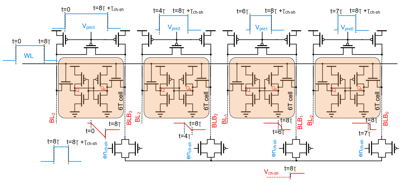
In this Section we discuss how to perform multiplication of 4-bit Vin by 4-bit W. The 4-bit W is stored within 4 adjacent 6T SRAM cells in a row as shown in Fig. 3 with MSB stored in the rightmost cell and LSB stored in the leftmost cell. In order to achieve multi-bit multiplication with respect to stored value W, the BLB discharge rate should dependent on bit significance, i.e. MSB bit leads to higher discharge as compared to LSB bit. Inducing such bit significance based discharge in conjunction to the discharge rate being proportional to enables multi-bit multiplication between Vin and W.
This requirement can be fulfilled through the pre-charge circuits that hold the BL and BLB to . We can disable the pre-charge circuit by making voltage equal to at different instant of time such that the BLB corresponding to the MSB bit starts discharging before the LSB bit. The ratio of time intervals for which MSB, 2nd bit, 3rd bit and LSB should discharge is 8:4:2:1. Thereby, by appropriately pulsing the pre-charge circuit, while is applied on the WL, would make the discharge on the BLBs proportional to their bit significance and to the input voltage . Interestingly, by enabling the signal after the BLBs have been given sufficient time to discharge, the four BLBs get connected to each other leading to charge sharing. This in turn ensures that the average discharge obtained from 4 BLBs (BLB3, BLB3, BLB1, and BLB0) is proportional to analog value of W as explained by equation 2. In the proportionality equation (2), w () is the analog equivalent of W.
| (2) | ||||

As mentioned in Section II-A, the pulse width of WL is and the amplitude of WL is dependent on , hence the intervals of discharge for BLB3, BLB3, BLB1 and BLB0 should be , , and respectively. If WL and signals are enabled at the instant say t=0, then , and are enabled at , and , respectively. At t=, signal is enabled and has a pulse width of . This enables charge sharing among BLB3, BLB3, BLB1 and BLB0. The voltage obtained after the charge sharing at the node is the analog multiplication result of 4-bit and 4-bit W. Timing diagram for various waveforms is shown in Fig. 4. In Fig. 4 we can see that there is a overlap between the WL signal and the precharge signal(). This means that there will be a static current flowing from the PMOS of the precharge through the access transistor. Next, we explain why static current does not play a significant role in the overall energy of the multiplication operation.
II-C Static Current
Multiplication operation in our approach is based on constant current discharge of the bit line as explained in Section II-A (Fig. 2). The bit line corresponding to the end of the latch storing ‘0’ will start discharging the bit line through the access transistor, while the other access transistor will remain switched off. In Section V-A we show that the internal node voltage of the SRAM cell is held close to the initial stored node voltage during the multiplication operation. Hence, the discharge current is mainly governed by the access transistor as the node storing ‘0’ is strongly held close to 0V by the NMOS transistor of the inverter latch. Further, to have a nearly constant current discharge we ensure that of the access transistors is large enough to operate in the constant current region of - characteristics. Therefore, we do not allow the bit line voltage to fall below a minimum voltage (), as mentioned in Section II-A, to have a high enough across the access transistor. Regarding the case where the WL signal and the precharge circuit have no overlap, BLB will discharge through the access transistors with a constant current. In this case, the charge stored on the bit line capacitance acts as source of power to facilitate constant current, this in effect reduces the voltage of capacitance at a constant rate. Due to channel length modulation effect the current through the access transistor not perfectly constant as the BLB voltage drops from 1200 mV to 350 mV, hence, to tackle this problem we change the pulse width of the precharge circuit to make the discharge at BLB3, BLB2, BLB1, and BLB0 in the ration 8:4:2:1 respectively. This approach is discussed in detail in IV-B.
The static current discharge path has a PMOS transistor of precharge circuit, NMOS access transistor and the NMOS transistor of the inverter latch. The PMOS transistor of the precharge circuit is strong enough to hold the bit line voltage close to 1.2V, when both the precharge and WL signals are enabled. Hence, the access transistor connected to the internal node storing logic low, has one of the end held to close to ground by the NMOS transistor of the inverter latch circuit, while the other end held close to 1.2V by the PMOS transistor of the precharge circuit. As a result, the current following through the access transistor and the NMOS transistor of the inverter latch is still governed by the access transistors. This current is equal to the fixed current that was discussed in the case where there was no overlap between the precharge circuit operation and the WL signal. This is due to the fact that the current through the access transistor is constant for ranging from 350 mV to 1200 mV and in this case is . The difference in this case is that the bit line capacitor maintains it’s charge and the constant current in this case is supplied by the power supply through the precharge circuit.
From the above two cases, it is clear that overlap between the operation of precharge circuit and the WL signal does not play a key role in terms of the energy consumption. Both the case dump equal amounts of charge to the ground if we neglect the channel length modulation effect of the access transistor. The difference in both the cases is that the case having the overlap in the operation of precharge and WL signal takes the charge form the power supply directly, while on the other hand the case where there is no overlap between the two operations takes the charge form the bit line capacitance which in turn is replenished by the supply during the next cycle of operation of precharge circuit. Our circuit simulations in spectre show constant and similar currents values for the of the NMOS transistor of the inverter latch for both the aforementioned case and justify the above explanation. In the next Section, we describe the array peripherals required to perform Multiply and Accumulate (MAC) operation.
III Peripheral Circuits
In this Section we explain the analog accumulator and the SAR-ADC in detail. Further, we provide provide the overall array architecture.
III-A Analog Accumulator

The accumulation circuit shown in Fig. 5 consist of a sample and hold circuit formed by a transmission gate (M7 and M8) and a sampling capacitor; a PMOS transistor (M9) and an accumulation capacitor. It is important to note that we use PMOS transistor instead of transmission gate for accumulating charge on the accumulation capacitor. Transistor M9 can only conduct when its overdrive voltage is positive, i.e. if 0V is applied at the gate of this transistor, it will only conduct when is greater than the threshold voltage of transistor M9(). If we are able to maintain the voltage of the accumulation capacitor less than for the entire process of accumulation period, then we can see that charge dumped on the accumulation capacitor would be . This charge is independent of the capacitor ratios or the initial charge/voltage on the accumulation capacitor. The increase in the voltage of accumulation capacitor would be given by:
| (3) |
Here, and represent the accumulation capacitor() and the sampling capacitor() respectively. Equation (3) holds true only if the following two conditions are met.
| (4) |
| (5) |
Here, n is the number of accumulations performed. Equations (4) and (5) are the design constrains which help us decide n, and the capacitor sizes used in the accumulation circuit. As analog accumulation unit was introduced to skip the ADC operation for every analog product. A high value of n is hence preferred as it leads to less frequent operation of ADC which in turn helps us save energy and improve the overall latency. On the other side, a high value of number of accumulations leads to a higher value accumulation capacitor evident from the above inequalities (4 and 5). A larger accumulation capacitor would occupy more area and would therefore limit the number of accumulations. A high value of number of accumulation also leads to degradation in software accuracy as the error in the analog value accumulated increases with number of accumulations. Further, the time taken for accumulation is 5 times the time taken for multiplication as seen in Table IV. Therefore, for the number of accumulations we explored the multiples of 5 to facilitate the multiplexing of ADC to further reduce the peripheral area if required. Hence, the number of accumulations(10) were chosen to be maximum provided the area and software accuracy are in acceptable limits. We keep the threshold voltage of transistor M9 to be high enough(600 mV) to allow larger values of n to satisfy the constrain equation (5) while not violating constrain equation (4). The sampling capacitor was kept to be the low (), so that the voltage at the node is almost equal to the voltage at the node and not a scaled version of . This means that the range of volatge at node is also 750 mV to 1200 mV. Using the value of , and n in constrain equation (5) we get when is kept as 1200 mV (voltage corresponding to maximum value of , when all parameter apart from is kept fixed). Hence we chose the accumulation capacitor to be 40 fF.
III-B Successive Approximation Register based ADC
The accumulated voltage is then converted to a digital output using a Successive Approximation Register ADC (SAR-ADC) as shown in Fig 6. Three components of this ADC are the sense amplifier, digital logic and the capacitor array based Digital to Analog Converter (DAC). The digital logic initializes the MSB of the ADC output to ‘1’, keeping all other bits ‘0’ and sends the digital code to DAC. The DAC converts this digital code to an analog voltage (). Subsequently, is compared against the input analog signal using a comparator. This is equivalent to comparing the input signal () to . If the input signal is higher than the DAC output (Compout is 0), MSB is kept at ‘1’ otherwise, it is flipped to ‘0’ which concludes 1 cycle of operation for SAR-ADC. In the consecutive cycle, the digital logic makes the next most significant bit ‘1’ keeping all the bits following it to be ‘0’. DAC converts the digital code to the analog signal which is compared against the input signal using the Sense Amplifier. The sense amplifier output is used to fix the bit under evaluation. The same process continues until all bits are evaluated. SAR-ADC takes n-cycles to evaluate the digital output, where n is the bit precision of the ADC. We adopt a capacitor array as the DAC and a standard sense amplifier as the comparator to reduce the static energy consumption in the utilized SAR-ADC. The target application of this work inspires the ADC bit-precision to be 4 bits with a conversion delay of 5 ns.

III-C Array Overview

The SRAM array for the proposed in-memory computing methodology is shown in Fig. 7. We adopt TSMC 65 nm technology node in our design. Additionally, we consider 50 fF bitline capacitance resulting from metal lines in layout.
The proposed array behaves as a conventional 6T-SRAM memory when and the analog multiplexer (MUX) are disabled and normal read/write operations are performed. Moreover, the circuit is capable of performing 4-bit4-bit multiplication and accumulation to provide a 4-bit output. The sign of the analog product is computed as XOR of the signs of both and W, and the product is accumulated on two different accumulation capacitors depending on the output sign. Furthermore, we share the circuit peripherals between two arrays to reduce the area penalty resulting for peripheral circuitry.
IV Circuit Simulation Results
In this Section we present circuit simulation results, wherein we analyse the non-linearity in the proposed multiplication circuitry and propose a mechanism to mitigate the non-linearity.
IV-A Linearity Analysis
The proposed multiplication circuitry, multiplies two scalars, namely, the input and the weight in an analog fashion. For the purpose of the linearity analysis we ignore the signs of both the input and the weight. This is because our approach computes the sign of the result depending on the signs of input and weight using digital gates and is free from any analog non-linearity. On the x-axis in Fig. 8 we have the ‘Expected Product’ or expected multiplication result for the digital multiplication of input and weight, while on y-axis we have the ‘Observed Product at (V)’ which is the analog product obtained at the node corresponding to input and the weight . For example, if the input is 5 and the weight is 10, then the x-coordinate for such a pair will be 50 (=5*10), while the y-coordinate will be the analog multiplication result obtained at by our proposed approach. We use spectre simulation to obtain the analog multiplication values as proposed in the paper. The SRAM bit cells are initialized to the weight value and input is provided to the input DAC. The DAC converts the input to an anlog value according to the equation 6. To multiply the two scalars and , proper signals were applied to precharge circuit (, , and ) and the charge sharing circuit (), as shown in Fig. 4. To multiply the two scalars and , proper signals were applied to precharge circuit (, , and ) and the charge sharing circuit (), as shown in Fig. 4.
| (6) |
For the plot shown in the Fig. 8, we keep the precharge pulse widths corresponding to , , , and such that the duration for which the BLB discharges are in the ratio 8:4:2:1 corresponding to BLB3, BLB2, BLB1 and BLB0 respectively (as shown in Fig. 4). However, with this approach we see from the scatter plot that the analog product obtained is non-linear and would require some correction techniques to mitigate the error. The possible options could be to have a non linear mapping for the input which would require design of a complicated DAC structure or non linear mapping of the weights which would require storing the non linear weights in the memory. In the next subsection we discuss how we mitigate this non linearity without having to use non-linear mapping.


IV-B Linearity Enhancement
We saw that the plot in Fig. 8 could be explained with four lines. This systematic non-linearity caused us to examine the analog multiplication even further. The approach followed to obtain results as shown in Fig. 8 is based on the assumption that the discharge of the BLB is the proportional to duration of discharge. However, we know that the access transistors in the SRAM bit cell are non-linear and hence the above assumption would no longer hold true. For equation (2) to hold, the discharge of BLB3, BLB2, BLB1 and BLB0 should be in ratio 8:4:2:1. Therefore, we keep the duration for which BLB3, BLB2, BLB1 and BLB0 discharge such that the discharge on the corresponding BLB is in the ratio 8:4:2:1 respectively. In other words, rather than keeping the duration of discharge in ratio 8:4:2:1, the discharge is kept in the ratio 8:4:2:1. To obtain the pulse width of , , , and pre0, we obtain the time taken by the BLB to discharge to 350 mV (minimum voltage for almost linear discharge as explained in Section II), 775 mV, 987.5 mV and 1093.75 mV respectively from 1.2V when the bit stored in bit cell is high which makes the discharge in the ratio 8(1200-350):4(1200-775):2(1200-987.5):1(1200-1093.75) respectively. For further analysis the ratios of the pre-charge pulse width are kept such that the BLB discharge ratio is 8:4:2:1.
In Fig. 10 (a) we present the analog multiplication output with varying and W = 0, 5, 10 and 15, similar trends were observed for other values of W. Similarly, in Fig. 10 (b) we observe the analog multiplication output with varying W and fixed to 0, 5, 10 and 15, similar trend observed for other values of . Fig. 10 (a) and Fig. 10 (b) show that digital output is directly proportional to the input voltage and the stored in the memory, respectively, confirming the multiplication operation of the proposed scheme. For Fig. 10 (a) the Integral Non-Linearity(INL) values for the W 0, 5, 10 and 15 are 1.1310-14, 1.1110-14, -4.8810-14 and 2.5510-14 respectively and INL values for 0, 5, 10 and 15 in Fig.10 (b) are 1.0910-14, 5.7710-14, -2.3610-14 and 3.10910-14 respectively.


Note, the accumulation voltage is always less than the threshold voltage of transistor M9 as discussed in section III-A. As a result, the analog accumulator behaves linearly by design. It is worth mentioning that the DAC block in ADC is designed to perform linearly during successive approximation by fine tuning the capacitor ratio. Additionally, the comparator is designed with an offset voltage as low as 5 mV, which is lower than the ADC precision, to ensure linearity.
V Variation Analysis
In this section we analyse the read stability of the SRAM cells to the ‘functional read’ in Subsection A. We study the effect of variations on the proposed circuitry considering random variations of the transistor threshold voltage in Subsection B and develop a framework presented in Subsection C to study the effects of such variations on the end application accuracy.
V-A Read Stability
To avoid read disturb we design the cell to have acceptable read noise margin, following a standard approach for SRAM cell design [11]. In our approach we only activate one WL at a time which further decreases the chances of corrupt read. When there is overlap between the WL signal and operation of the precharge, both BL and BLB are held high by the precharge circuit and hence the differential signal applied to the cell is zero which ensure that the data stored in the cell is not corrupted by the multiplication operation. When the precharge circuit is disabled, while the WL signal is still high, the circuit performs normal conventional read and discharges BL or BLB depending on data stored in bit cell. Many in-memory compute primitives [12], [7], [13] have shown similar kind of functional read operations where they connect the internal storage node to the bit line in order to enable analog in-memory compute.
In order to understand the read disturb that could arise due to analog multiplication operation as proposed in our approach, we need to understand the differences in our approach and the conventional memory read operation. In our approach, we have an overlap between the operation of precharge circuit and the WL signal for certain bits of weights, as seen in waveforms shown in Fig. 4. The case where the precharge circuit operation and WL signal have no overlap, as in the case of , the operation is similar to conventional memory read operation. On the other hand, when the precharge circuit operation and WL signal have maximum overlap as seen in the case of , is different from the conventional read case and requires further analysis. We also use analog signal on the WL which is different from the conventional read operation. The worst case WL signal amplitude would be 1 V, which is the strongest connection between the internal node and the bit line. Hence, we analyse the case where the amplitude of WL signal is 1 V and there is maximum overlap between the operation of the precharge circuit and the WL signal.
To study the read disturb for these conditions, we simulate two SRAM bit cells with the precharge circuit and initialize the two cells to store opposite bits(one storing digital high and other storing digital low). We perform 10000 Monte Carlo runs, on the two SRAM cells, having the WL amplitude 1V and setting the precharge signal to and monitor the number of times the bit stored in the internal node switches. We find that none of the cells flip there initial stored states. Further, the maximum change in voltage during the functional read operation at node storing digital low (0 V) is 95.56 mV and maximum change in the node storing digital high (1 V) is 51.91 mV. This analysis shows that the proposed SRAM in memory multiplication approach is robust to read disturbs.
V-B Variations in Multiplication In-memory
Random variations of access transistor threshold voltage are one of the major causes of performance degradation in circuit design. In the proposed circuit, the mismatch between BLB access transistors of the 4 adjacent SRAM cells, shown in Fig. 3, can cause erroneous output. Such output errors happen because the rate of discharge for BLB3, BLB2, BLB1 and BLB0 are no longer proportional to 8:4:2:1 for the same value of input . We perform Monte Carlo runs using the TSMC 65 nm PDK to simulate the random variations in the proposed circuitry. The maximum standard deviations for the analog multiplication output in 1000 Monte Carlo runs is seen to be 13.17 mV.
To assess the effect of variations on the digital output we run 1000 samples of Monte Carlo simulation on the entire circuit consisting of SRAM array and the peripheral circuits including the ADC. The simulation results for a chosen set of cases where the digital output is 0,3,6,8,11 and 15 are shown in Fig. 11. Notice that the maximum standard deviation of the Gaussian curve for digital output was 0.6. From Fig. 11 we see that the distributions for digital output 0 and 15 are truncated Gaussian distributions. The reason for that is the ADC being only able to map the input voltage in its predefined range of conversion. Any voltage below the range of conversion is mapped to 0 and any voltage above the range of conversion would be mapped to 15.

V-C Functional Accuracy Analysis
We test the proposed multiplication and accumulation engine on a convolutional neural network shown in Table I for classifying Cifar10 dataset. We refer to [14] for the training framework. The network is trained using Adam optimizer with initial learning rate of 0.0001 for 200 epochs. The learning rate is dropped by a factor of 10 at epoch number 100, 150 and 180. The training batch size and testing batch size is 32 and 128 respectively. We perform small data augmentation (Flipping the training dataset and shifting the training dataset by 4 pixels). Cross-entropy loss function is adopted for training, while the test accuracy for such network is 91.50%. Now, in order to assess the effect of hardware non ideal effects we first run the neural network with quantized weights and activation with the weights and activations being quantized separately for each layer of the network. Using linear quantization, the minimum number of bits required to represent activations and weights is 5-bits to get acceptable accuracy of 90.91%. Moreover, we add an effective multiplication error to the output map sampled from a Gaussian distribution of circuit variation sigma equal to 0.6, where n is number of 10 element MAC operations and standard deviation for individual multiplication from the variation analysis was taken to be 0.6 following a pessimistic approach. For inference, we sample the errors from the Gaussian distribution for each output map and keep it constant for that particular inference as the error is dependent on the location where the weight is written and is fixed once the weight is stored in SRAM. We run 1000 inferences adding error to the output map as described above, the test accuracy remains between 88.83%-89.62% (mean=89.25% and sigma=0.1329) with circuit variations.
| Layer | Input Map | Output Map | Non Linearity |
|---|---|---|---|
| 64 3x3 Conv1 | 32x32x3 | 32x32x64 | ReLU,dropout(0.3) |
| 64 3x3 Conv2 | 32x32x64 | 32x32x64 | ReLU |
| [2 2] MaxPool1 | 32x32x64 | 16x16x64 | - |
| 128 3x3 Conv3 | 16x16x64 | 16x16x128 | ReLU,dropout(0.4) |
| 128 3x3 Conv4 | 16x16x128 | 16x16x128 | ReLU |
| [2 2] MaxPool2 | 16x16x128 | 8x8x128 | - |
| 256 3x3 Conv5 | 8x8x128 | 8x8x256 | ReLU,dropout(0.4) |
| 256 3x3 Conv6 | 8x8x256 | 8x8x256 | ReLU,dropout(0.4) |
| 256 3x3 Conv7 | 8x8x256 | 8x8x256 | ReLU |
| [2 2] MaxPool3 | 8x8x256 | 4x4x256 | - |
| 4096x4096 FC1 | 1x1x4096 | 1x1x4096 | ReLU,dropout(0.5) |
| 4096x4096 FC2 | 1x1x4096 | 1x1x4096 | ReLU,dropout(0.5) |
| 4096x10 FC3 | 1x1x4096 | 1x1x10 | - |
Most of the recent in-memory work in literature are designed to run neural networks against the MNIST dataset. We use our network model to classify MNIST dataset on a vanilla LeNet network. For this task full precision test accuracy is found to be 99.3%, quantized (4-bit activation and 4-bit weights) test accuracy is 99.24% and test accuracy for our approach remains between 99.05% to 99.32% (mean=99.19% and sigma=0.0398) for 1000 variation-affected inference runs.
VI System level Analysis
| Related Work | Process (nm) | SRAM Array | Cell Area | Computation Nature | Input/Weight precision | Dataset | Network Architecture | Accuracy | Energy |
|---|---|---|---|---|---|---|---|---|---|
| IMAC | 65 | 6T | 1x | Analog | 5/5 | Cifar10 MNIST | VGG LeNet-5 | >88.83% >99.05% | - 158.203 nJ (/inference) |
| [12] | 65 | 6T | 1x | Analog | 6/4 | MNIST | LeNet-5 | >97% | 359.288 nJ (/inference) |
| [15] | 45 | 8T | 1.68x | Analog | -/4 | MNIST | MLP | 98.15% | 180 pJ (/1616 MAC) |
| [16] | 28 | 8T | 1.3x | Analog | 8/1 | ImageNet | AlexNet | <1% drop | 12.8-119.7 TOPS/W |
| [17] | 65 | 12T | 2x | Analog | ternary/1 | Cifar10 MNIST | BNN[18] MLP | 85.7% 98.3% | 2.48-7.19 fJ (/operation) |
| [19] | 55 | Twin-8T | 1.4x | Digital | 4/5 | Cifar10 MNIST | CNN CNN | 90.42% 99.52% | 11.7 pJ (/unit-Macro (6460 bits)) |
| [9] | 28 | 6T | 1x | Digital | 8/8 | ImageNet | Inception V3 | - | 0.246 J (/inference) |


In this section we compare the proposed work with a standard von Neumann architecture which is considered as our baseline. For conventional von Neumann architecture a neural network application can be broken down into Read, Multiply, Accumulate and non-linearity(ReLU in our case) kernels. It is worth mentioning that the ReLU operation energy consumption can be neglected compared to other operations. The delay () and the energy () of convolution operation in the conventional von Neumann architecture are given by equation (7) and (8) similar to [12]. The notations used in the equations below are described in Table III. We can obtain the formula for fully connected layer by simply making the input size(L) and kernel size(K) as 1. In the fully connected layer M and N denote the number of input and output neurons respectively.
| (7) |
| (8) |
The delay() and energy() for convolution operation involving in-memory multiplication operation as described in this work is given by equation (9) and (10) respectively.
| Notation | Description |
|---|---|
| M | number of input Feature Maps |
| N | number of output Feature Maps |
| K | Kernel size KK |
| L | Size of input feature map LL |
| Size of output feature map () | |
| bits fetched from SRAM to processor per bank | |
| bit width of the weight stored in SRAM | |
| number of columns in SRAM array | |
| number of SRAM banks | |
| number of multipliers in processor | |
| time required to fetch data from SRAM to processor | |
| time required to perform multiplication in processor | |
| time required for 1 in memory analog multiply and accumulation | |
| time required for adc operation | |
| energy required to fetch data from SRAM to processor | |
| energy required to perform multiplication in processor | |
| energy required for 1 in memory analog multiply and accumulation | |
| energy required for adc operation | |
| R | number of MAC performed in analog domain |
| Standby power consumption of SRAM memory |
| (9) |
| (10) |
| Parameter | Value | Parameter | Value |
|---|---|---|---|
| 16-256 | 5 | ||
| 4 | / | 256 | |
| 175 | |||
| 5.2 pJ | 4 ns | ||
| 0.9 pJ | 4 ns | ||
| 0.254 pJ | 1 ns | ||
| 0.253 pJ | 5 ns | ||
| 2.4 nW | R | 10 |
| Component | Total area per array (m2) |
|---|---|
| SRAM cell | 83100 |
| ADC | 40800 |
| Accumulator | 30600 |
| DAC | 400 |
| MUX | 2100 |
| Decoder | 4800 |
| Column circuit | 44000 |
For a fair comparison, all array parameters are kept the same as [12] and delay and energy parameters are obtained from circuit simulations. The parameters used are presented in Table IV. Fig. 13 compares the energy, delay and the Energy delay product of this work against baseline. From Fig. 13, the total improvements in energy, delay and energy-delay product are seen to be 9.42, 6.24 and 58.79 respectively. Since the array architecture for this work is kept similar to [12], we compare the Energy and Delay of this work and find this work to be 2.27 and 4.83 better than [12]. Table II compares this work with other similar in-memory computing works. The plot show in Fig. 13 compare the EDP improvements of this work against von Neumann for different . EDP of this work is 22 better than von Neumann, even when is made 256. The area estimates for individual blocks are presented in the Table V. It can be seen that 36% of the total array area would be occupied by the peripherals introduced in this work.
VII Conclusion
In this work we present an in-memory dot product computing primitive using standard 6T SRAM arrays. We encode the input () signal as an analog voltage on the wordline, while the bit significance of the stored input (W) is encoded using precharge pulse. We perform analog accumulation to reduce the use of energy expensive ADC. We also perform detailed circuit analysis including random transistor variations to study the effects of such non-idealities on application accuracy. We develop a circuit-software co-simulation framework including circuit non-idealities and show an accuracy of 88.83% and 99.05% on CIFAR-10 and MNIST datasets, respectively. Additionally, we evaluate the proposed in-memory compute primitive to compare the system delay/energy with state-of-the-art neural network in-memory accelerators. The proposed system is 58.78 and 8 better in EDP than the standard von Neumann system and recent neural network accelerator, respectively.
References
- [1] M. Gokhale, B. Holmes, and K. Iobst, “Processing in memory: The terasys massively parallel pim array,” Computer, vol. 28, no. 4, pp. 23–31, 1995.
- [2] D. G. Elliott, W. M. Snelgrove, and M. Stumm, “Computational ram: A memory-simd hybrid and its application to dsp,” in Custom Integrated Circuits Conference, 1992., Proceedings of the IEEE 1992. IEEE, 1992, pp. 30–6.
- [3] A. Agrawal, A. Jaiswal, C. Lee, and K. Roy, “X-sram: Enabling in-memory boolean computations in cmos static random access memories,” IEEE Transactions on Circuits and Systems I: Regular Papers, no. 99, pp. 1–14, 2018.
- [4] S. Aga, S. Jeloka, A. Subramaniyan, S. Narayanasamy, D. Blaauw, and R. Das, “Compute caches,” in 2017 IEEE International Symposium on High Performance Computer Architecture (HPCA). IEEE, 2017, pp. 481–492.
- [5] M. Kang, M.-S. Keel, N. R. Shanbhag, S. Eilert, and K. Curewitz, “An energy-efficient vlsi architecture for pattern recognition via deep embedding of computation in sram,” in Acoustics, Speech and Signal Processing (ICASSP), 2014 IEEE International Conference on. IEEE, 2014, pp. 8326–8330.
- [6] Q. Dong, S. Jeloka, M. Saligane, Y. Kim, M. Kawaminami, A. Harada, S. Miyoshi, D. Blaauw, and D. Sylvester, “A 0.3 v vddmin 4+ 2t sram for searching and in-memory computing using 55nm ddc technology,” in 2017 Symposium on VLSI Circuits. IEEE, 2017, pp. C160–C161.
- [7] J. Zhang, Z. Wang, and N. Verma, “In-memory computation of a machine-learning classifier in a standard 6t sram array,” IEEE Journal of Solid-State Circuits, vol. 52, no. 4, pp. 915–924, 2017.
- [8] S. K. Gonugondla, M. Kang, and N. R. Shanbhag, “A variation-tolerant in-memory machine learning classifier via on-chip training,” IEEE Journal of Solid-State Circuits, no. 99, pp. 1–11, 2018.
- [9] C. Eckert, X. Wang, J. Wang, A. Subramaniyan, R. Iyer, D. Sylvester, D. Blaauw, and R. Das, “Neural cache: bit-serial in-cache acceleration of deep neural networks,” in Proceedings of the 45th Annual International Symposium on Computer Architecture. IEEE Press, 2018, pp. 383–396.
- [10] M. Kang, S. K. Gonugondla, A. Patil, and N. R. Shanbhag, “A multi-functional in-memory inference processor using a standard 6t sram array,” IEEE Journal of Solid-State Circuits, vol. 53, no. 2, pp. 642–655, Feb 2018.
- [11] D. Mukherjee, H. K. Mondal, and B. Reddy, “Static noise margin analysis of sram cell for high speed application,” International Journal of Computer Science Issues (IJCSI), vol. 7, no. 5, p. 175, 2010.
- [12] M. Kang, S. Lim, S. Gonugondla, and N. R. Shanbhag, “An in-memory vlsi architecture for convolutional neural networks,” IEEE Journal on Emerging and Selected Topics in Circuits and Systems, vol. 8, no. 3, pp. 494–505, Sep. 2018.
- [13] Jintao Zhang, Zhuo Wang, and N. Verma, “A machine-learning classifier implemented in a standard 6t sram array,” in 2016 IEEE Symposium on VLSI Circuits (VLSI-Circuits), June 2016, pp. 1–2.
- [14] J. T. Springenberg, A. Dosovitskiy, T. Brox, and M. A. Riedmiller, “Striving for simplicity: The all convolutional net,” CoRR, vol. abs/1412.6806, 2014.
- [15] A. Jaiswal, I. Chakraborty, A. Agrawal, and K. Roy, “8t sram cell as a multibit dot-product engine for beyond von neumann computing,” IEEE Transactions on Very Large Scale Integration (VLSI) Systems, pp. 1–12, 2019.
- [16] J. Yang, Y. Kong, Z. Wang, Y. Liu, B. Wang, S. Yin, and L. Shi, “24.4 sandwich-ram: An energy-efficient in-memory bwn architecture with pulse-width modulation,” in 2019 IEEE International Solid- State Circuits Conference - (ISSCC), Feb 2019, pp. 394–396.
- [17] Z. Jiang, S. Yin, M. Seok, and J.-s. Seo, “Xnor-sram: In-memory computing sram macro for binary/ternary deep neural networks,” in 2018 IEEE Symposium on VLSI Technology. IEEE, 2018, pp. 173–174.
- [18] M. Courbariaux, I. Hubara, D. Soudry, R. El-Yaniv, and Y. Bengio, “Binarized Neural Networks: Training Neural Networks with Weights and Activations Constrained to +1 or − 1,” arXiv., 2016.
- [19] X. Si, J. Chen, Y. Tu, W. Huang, J. Wang, Y. Chiu, W. Wei, S. Wu, X. Sun, R. Liu, S. Yu, R. Liu, C. Hsieh, K. Tang, Q. Li, and M. Chang, “A twin-8t sram computation-in-memory unit-macro for multibit cnn-based ai edge processors,” IEEE Journal of Solid-State Circuits, vol. 55, no. 1, pp. 189–202, Jan 2020.
![[Uncaptioned image]](2003.12558v1/mustafa_ali.jpg) |
Mustafa Ali received his B.Sc. ans M.Sc. degrees in Electrical Engineering from MTC, Cairo, Egypt in 2011, 2016 respectively. He achieved the 1st rank in undergraduate in MTC, 2011. He was honored the Duty Medal for excellent performance during his studies. He worked on flexible electronics applications using TFTs in his M.Sc from 2014 to 2016. Additionally, he worked as a TA and RA at MTC from 2013 to 2017. Mustafa was also a hardware and embedded systems engineer at Integreight, Inc. from 2012 to 2017. He joined the Nano-electronics Research Lab (NRL), Purdue University in Spring 2018 and he is currently pursuing his Ph.D. under the guidance of Prof. Roy. His research interest lies in accelerating Brain-inspired Computing and machine learning. He is also interested in in-memory computing based on CMOS and post-CMOS devices. |
![[Uncaptioned image]](2003.12558v1/akhilesh_jaiswal.jpg) |
Akhilesh Jaiswal received the B.Tech. degree from Shri Guru Gobind Singhji Institute of Engineering and Technology, Nanded, India, in 2011, the M.S. degree in electrical engineering from the University of Minnesota, Minneapolis, MN, USA, in 2014 and PhD in electircal and communication engineering from Purdue University, West Lafayete, USA, in 2019. He joined the Globalfoundries Laboratory, Malta, NY, USA in 2019. He was an Intern at the Globalfoundries Laboratory, Malta, NY, USA, in 2017. His current research interests include modeling and simulation of spin devices for on-chip memory/logic/nueromorphic applications, and neuromorphic applications using analog and digital CMOS circuits. Besides he is also interested in in-memory computing based on emerging and CMOS devices. |
![[Uncaptioned image]](2003.12558v1/kodge.jpg) |
Sangamesh Kodge received the B.Tech. degree in electrical engineering from IIT Kharagpur, Kharagpur, India , in 2018. During his tenure at IIT Kharagpur, he has received Institute Silver medal, Rajender Kumar Khanna Memorial prize on being adjudged to be the best student in the order of merit and System Society Award for the best project on systems. He was a research intern and NTU-India Connect Fellow at Nanyang Technological University (NTU), Singapore in 2017. He joined Nanoelectronics research lab at Purdue in fall 2018 and is currently pursuing his PhD under the guidance of Prof. Kaushik Roy. His primary research interest lie in brain-inspired computing, explanable machine learning and theoretical machine learning. |
![[Uncaptioned image]](2003.12558v1/Amogh.png) |
Amogh Agrawal received the B.Tech degree in electrical engineering from the Indian Institute of Technology, Ropar, India in 2016. He was a research intern at University of Ulm, Germany in 2015, under the DAAD (German Academic Exchange Service) Fellowship. He joined the Nanoelectronics research lab in 2016, and is currently pursuing his PhD degree at Purdue University under the guidance of Prof. Kaushik Roy. He was a Technology Development Intern at GLOBALFOUNDRIES, Malta, NY, USA, during the summer of 2018.His primary research interests include modeling and simulation of spin devices for application in logic, memories and neuromorphic computing. He is also looking at in-memory computing techniques for neuromorphic computing using CMOS and beyond-CMOS memories. He was awarded the Directors Gold Medal for his all-round performance, and University Silver Medal for his academic achievements at IIT Ropar. He is a recipient of the Andrews Fellowship from Purdue University, in 2016. |
![[Uncaptioned image]](2003.12558v1/indranil.jpeg) |
Indranil Chakraborty received the B.Engg. degree in Electronics and Telecommunication Engineering from Jadavpur University, Kolkata, India, in 2013, and the M.Tech. degree in Electrical Engineering from Indian Institute of Technology Bombay, Mumbai, India, in 2016. He was the recipient of best M. Tech thesis award and academic excellence award during his time at IIT Bombay for his academic performance. Since Fall 2016, he has been pursuing the Ph.D. degree with the Nanoelectronics Research Laboratory, Purdue University, West Lafayette, IN, USA. His primary research interests lie in hardware for machine-learning using CMOS and emerging technologies. |
![[Uncaptioned image]](2003.12558v1/kaushik.jpg) |
Kaushik Roy received the B.Tech. degree in electronics and electrical communications engineering from IIT Kharagpur, Kharagpur, India and the Ph.D. degree from the Department of Electrical and Computer Engineering, University of Illinois at Urbana-Champaign, Champaign, IL, USA,in 1990. He was with the Semiconductor Process and Design Center, Texas Instruments, Dallas, TX, USA, where he was involved in field-programmable gate array architecture development and low-power circuit design. He was a Faculty Scholar at Purdue University, West Lafayette, IN, USA, from 1998 to 2003. He was a Research Visionary Board Member of Motorola Labs in 2002. He held the M. K. Gandhi Distinguished Visiting Faculty, IIT Bombay, Mumbai, India. He joined the Electrical and Computer Engineering Faculty, Purdue University, West Lafayette, IN, USA, in 1993,where he is currently an Edward G. Tiedemann Jr. Distinguished Professor. He has authored over 600 papers in refereed journals and conferences, holds 15 patents, graduated 60 Ph.D. students, and is a coauthor of two books: Low-Power CMOS VLSI Circuit Design (New York, NY, USA: Wiley, 2009) and Low Voltage, Low Power VLSI Subsystems (New York, NY, USA: McGraw-Hill, 2005). His current research interests include spintronics, device circuit codesign for nanoscale silicon and nonsilicon technologies, low-power electronics for portable computing and wireless communications, and new computing models enabled by emerging technologies. Dr. Roy received the U.S. National Science Foundation Career Development Award in 1995, the IBM Faculty Partnership Award, the ATT/Lucent Foundation Award, the 2005 SRC Technical Excellence Award, the SRC Inventors Award, the Purdue College of Engineering Research Excellence Award, the Humboldt Research Award in 2010, the 2010 IEEE Circuits and Systems Society Technical Achievement Award, the Distinguished Alumnus Award from IIT Kharagpur, the Fulbright-Nehru Distinguished Chair, and best paper awards at the 1997 International Test Conference, the IEEE 2000 International Symposium on Quality of IC Design, the 2003 IEEE Latin American Test Workshop, the 2003 IEEE Nano, the 2004 IEEE International Conference on Computer Design, the 2006 IEEE/ACM International Symposium on Low Power Electronics & Design, and the 2005 IEEE Circuits and System Society Outstanding Young Author Award (Chris Kim), the 2006 IEEE Transactions on VLSI Systems Best Paper Award, the 2012 ACM/IEEE International Symposium on Low Power Electronics and Design Best Paper Award,the 2013 IEEE Transactions on VLSI Best Paper Award. He has been on the Editorial Board of IEEE DESIGN AND TEST, the IEEE TRANSACTIONS ON CIRCUITS AND SYSTEMS, the IEEE TRANSACTIONS ON VERY LARGE SCALE INTEGRATION(VLSI) SYSTEMS, and the IEEE TRANSACTIONS ON ELECTRON DEVICES. He was the Guest Editor for the Special Issue on Low-Power VLSI in IEEE DESIGN ANDTESTin 1994 and the IEEE TRANSACTIONS ON VERY LARGE SCALE INTEGRATION (VLSI) SYSTEMS in 2000, the IEE Proceedings-Computers and Digital Techniques in 2002, and the IEEE JOURNAL ON EMERGING AND SELECTED TOPICS IN CIRCUITS AND SYSTEMS in 2011. |