Analysis of Magnetic Vortex Dissipation in Sn-Segregated Boundaries in Nb3Sn Superconducting RF Cavities
Abstract
We study mechanisms of vortex nucleation in Nb3Sn Superconducting RF (SRF) cavities using a combination of experimental, theoretical, and computational methods. Scanning transmission electron microscopy (STEM) image and energy dispersive spectroscopy (EDS) of some Nb3Sn cavities show Sn segregation at grain boundaries in Nb3Sn with Sn concentration as high as 35 at.% and widths 3 nm in chemical composition. Using ab initio calculations, we estimate the effect excess tin has on the local superconducting properties of the material. We model Sn segregation as a lowering of the local critical temperature. We then use time-dependent Ginzburg-Landau theory to understand the role of segregation on magnetic vortex nucleation. Our simulations indicate that the grain boundaries act as both nucleation sites for vortex penetration and pinning sites for vortices after nucleation. Depending on the magnitude of the applied field, vortices may remain pinned in the grain boundary or penetrate the grain itself. We estimate the superconducting losses due to vortices filling grain boundaries and compare with observed performance degradation with higher magnetic fields. We estimate that the quality factor may decrease by an order of magnitude ( to ) at typical operating fields if 0.03% of the grain boundaries actively nucleate vortices. We additionally estimate the volume that would need to be filled with vortices to match experimental observations of cavity heating.
I introduction
Superconducting Radio-Frequency (SRF) cavities are used in accelerators to transfer energy to beams of charged particles. Oscillating electric fields induce magnetic fields parallel to the surface of the cavity. However, for very large induced magnetic fields, the superconducting Meissner state is unstable, so that a fundamental limit to the cavity’s performance is the material’s ability to expel large magnetic fields. For type-II materials, complete flux expulsion is thermodynamically stable up to a lower-critical field, , and a mixed state characterized by superconducting vortices is stable for fields up to an upper-critical field, . Thus, by limiting the fields on the walls of the SRF cavities, the superconductor can be kept in the flux-free Meissner state, so that surface dissipation is extremely small and quality factors can be achieved. For magnetic fields parallel to the cavity surface, the superconducting Meissner state can be maintained above the stability limit in a metastable state up to a limit (for an ideal surface) of the so-called superheating field Liarte et al. 2017. has been studied extensively by the condensed matter community, primarily in the context of Ginzburg-Landau theory at ideal interfacesTranstrum et al. 2011; Chapman 1995; Dolgert et al. 1996; Kramer 1968a. Because high-power SRF cavities routinely operate in the metastable regimePosen et al. 2015, there has been renewed interested by the condensed matter community in the behavior of superconductors in large magnetic fields. Calculations extend results to the semi-classical theory of Eilenberger theory in both the cleanCatelani and Sethna 2008 and dirtyLin and Gurevich 2012 limits and Time-Dependent Ginzburg Landau (TDGL) simulations that account for materialPack et al. 2019 and spatial inhomogeneitiesAladyshkin et al. 2001; Burlachkov et al. 1991; Vodolazov 2000; Soininen and Kopnin 1994. In this paper, we explore the role of grain boundaries (GBs) in SRF cavity performance motivated by experimental observations of inhomogeneities in real-world SRF cavities. It is well-established that grain boundaries can strongly affect the superconducting properties of Nb3Sn. They are known to pin vortices and determine critical currents in Nb3Sn wiresScanlan et al. 1975; Godeke 2006. Compositional variation within Nb3Sn grain-boundaries on the scale of a few nanometers have been observedSuenaga and Jansen 1983; Sandim et al. 2013. This study brings together the expertise of many areas of condensed matter and accelerator physics to explore fundamental physics of superconductors in extreme conditions and connect those results to real systems.
Recently there has been significant progress towards the employment of Nb3Sn in SRF cavities as a higher performance alternative to the industry standard Nb for next generation particle accelerator applications Posen and Hall 2017; Posen and Liepe 2014. Nb3Sn cavities are prepared with Nb3Sn films 2 m (nearly 20 penetration depths) thick coated on the surface of Nb cavities using the Sn vapor-diffusion process. Nb3Sn is an intermetallic alloy with A15 crystal structure; it is a promising material for next-generation SRF cavities in large part because of its large (predicted) superheating field (400 mT). It also has a higher critical temperature (Tc 18K), making possible a higher quality factor (Q0, another critical metric of cavity performance) at a given temperature compared to Nb (Tc 9K).
In practice, however, real world Nb3Sn cavities quench well below the theoretically predicted value. The maximum accelerating gradient that has been achieved within these cavities is about 24 MV/m, which corresponds to the surface magnetic field of 98 mT. These cavities exhibit a high Q0 of at 4.2 K Posen and Hall 2017; posen2019nb3sn; however, in some cavities, Q0 begins to degrade significantly before the limiting quench field is reached, a phenomenon described as “Q-slope”Müller et al. 2000.
Understanding the mechanism underlying the Q-slope phenomenon is an important question for cavity development. Several mechanisms have been proposed in terms of imperfections in the Nb3Sn coatings Gurevich 2017; Hall 2017; Posen et al. 2015 such as thin grains Lee et al. 2018; Trenikhina et al. 2017 and Sn-deficient regions Becker et al. 2015. Another potential mechanism that may have detrimental effects on the performance of Nb3Sn cavities is Sn segregation at grain boundaries Lee et al. 2020. In some Nb3Sn coatings, tin concentrations as high as 35 at.% have been observed in grain boundaries with the segregated zone extending by as much as 3 nm, comparable to the coherence length of Nb3Sn (3 nm). Because of the inferior superconducting properties, magnetic flux may penetrate the segregated region, degrade Q0, and lead to premature quench.
In support of this hypothesis, witness samples coated with high-performance (quench at 24 MV/m with Q1010 at 4.4 K) Nb3Sn cavities at Fermilab did not show Sn segregation at the grain boundaries in energy dispersive X-ray spectroscopy (EDS) and in scanning transmission electron microscopy (STEM). Similarly, a direct cutout from a high-performance Nb3Sn cavity fabricated at Cornell did not show Sn segregation at grain boundaries within the detection limit of STEM-EDS. In contrast, Nb3Sn cavities, which show Sn segregation at grain boundaries in witness samples coated together with the cavities, displayed negative Q-slope for accelerating fields in the 5-15 MV/m range, see Fermilab cavity 1 and 2, Fig. 1. These experimental results, summarized in Fig. 1, suggest a potential link between Sn segregation at grain boundaries and cavity performance Lee et al. 2020.

Experimentally, it is difficult to isolate the effects of Sn segregation at grain boundaries from other imperfections, such as Sn-deficient regions and surface roughness. To overcome these challenges, we use numerical tools to theoretically understand the role of segregation in grain boundaries for SRF cavity performance. We use density functional theory to estimate the effective of the material within the segregation zone. Next, we use time-dependent Ginzburg-Landau simulations with spatial varying material properties motivated by the ab initio DFT calculations. Time-dependent Ginzburg-Landau theory allows us to conduct numerical experiments on a mesoscale that probe the role of grain boundaries and segregated zones for vortex nucleation, pinning, and quenching. Finally, motivated by our TDGL simulations, we estimate power dissipated by vortex nucleation within segregated grain boundaries during an RF cycle and make quantitative comparisons to actual SRF cavities.
This paper is organized as follows: First, we present experimental and first-principles analyses of grain-boundary defect segregation in Nb3Sn cavities in section II. We then report on first principles DFT calculations of superconducting properties for segregation zones in section III and time-dependent Ginzburg-Landau simulations of flux penetration in section IV. We estimate the effect on cavity performance in section V. Our numerical experiments isolate the effects of Sn-segregated grain boundaries from potentially confounding mechanisms. Our results indicate that the effects of Sn-segregated grain boundaries alone are consistent with observed behaviors. Specifically, grain boundaries may nucleate and then trap a limited number of vortices, leading to degradation in the cavity’s quality factor. We conclude by discussing the implications of these results for cavity development and further theoretical studies in section VI.
II Experimental and Theoretical Study of Nb3Sn Defect Segregation
We have systematically investigated the composition of GBs in Nb3Sn coatings and the origin of Sn-segregation at GBs using experimental and first-principles methods. The high angle annular dark field (HAADF)-STEM image in Figure 2 displays a Nb3Sn coating on Nb prepared by the Sn vapor diffusion process using coating parameters from the early stage of the development of Nb3Sn films at Fermilab Posen and Hall 2017. EDS mapping is performed across a GB in a Nb3Sn coating prepared by the same coating parameters and reveals that Sn is segregated at the GB, Figure 3. The maximum concentration of Sn at the GB is 33 at.% and the width of the Sn segregated region is 3 nm. The Gibbsian interfacial excess of Sn is 16 atom/nm2. Previous analyses of the structures of Sn-segregated GBs in Nb3Sn employing HR-STEM and first-principle calculations indicated that most of the segregated Sn exist as Sn-antisite defects near the GBs rather than forming Sn-rich phases such as Nb6Sn5 or other non-equilibrium phases Lee et al. 2020; Dillon et al. 2007. Another GB from a witness sample of a high-performance cavity, which is prepared by the coating procedure with less Sn and higher furnace temperature than the previous coating to mitigate the Sn-segregation at GBs Lee et al. 2020, is characterized by HR-STEM EDS, Fig. 4. It is noted that there is no Sn segregation at the GB within the detection limit of EDS (1 at.%). This indicates a possible correlation between the Sn segregation at GBs and cavity performance, and motivates us to investigate the effects of Sn-segregation on GB properties using DFT and Ginzburg-Landau calculations.
To investigate the origin of the Sn-segregation in the Nb3Sn coating, we consider our previous experimental study of Nb3Sn GBs using STEM-EDS and APT analyses Lee et al. 2020. Nine batches of coatings were characterized by randomly selecting 2-4 GBs as representatives for each coating and analyzing them. Our results show that the effect of the GB structure (characterized by five degrees of freedom given by the rotation axis (c), the disorientation angle (), and the normal vector to the GB plane (n)) on Sn-segregation is insignificant, which is in contrast with the usual behavior of GB segregation behaviors of alloys in an equilibrium state Seidman 2002; Rittner et al. 1997. Even small-angle GB reveal a similar amount of Sn-segregation at GBs to high-angle GBs nearby. In parallel, we performed a detailed DFT study surveying a variety of GB structures in Nb3Sn including both symmetric tilt and twist GBs, identifying a number of low energy structures Kelley et al. 2020. We found a rapid decay of local strain while moving away from the GB, and a disruption to the electronic structure that decays to bulk behavior 1–1.5 nm from the GB. Importantly, this disruption reduces the Fermi-level density-of-states by more than a factor of 2 in the core region. Associated with this density-of-states reduction, we also found a strong binding of tin on niobium antisite defects to GBs that extends outward to the same distances of 1–1.5 nm.
Based on these results, we consider both kinetic and thermodynamic factors that may contribute to Sn-segregation at GBs. For the kinetic factor, we considered the Sn-diffusion process along GBs, and it is found that the amount of Sn-segregation at GBs in Nb3Sn is affected by Sn-flux during the coating process: higher Sn-flux causes a more significant amount of Sn-segregation at GBs. This suggests that the kinetic Sn GB diffusion process plays a significant role in determining the chemical composition of GB. For the thermodynamic factor, the attractive electronic interaction between Sn-antisite defects and GBs may also play an important role, as we find that this interaction has a range similar to the observed radius of Sn-segregation, and depends only weakly on the structure of the GB. The current coating procedures at Fermilab and Cornell successfully mitigates the Sn-segregation at GBs by annealing without the external Sn-source Kempshall et al. 2002.
Finally, we observe divots in the Nb3Sn surface at GBs; the HAADF-STEM image in Fig. 5 displays the geometry of a GB on the top surface. It has 80 nm of depth and 420 nm of width. The unique compositional and geometrical changes at GBs may provide pathways for flux to penetrate the surface. This observations motivates us to consider surface geometry as an additional factor in our Ginzburg-Landau modeling of vortex penetration.


III The effect of tin-rich stoichiometry on
Previous works have demonstrated that both defects and strain can reduce the of Nb3Sn, and that this effect can be attributed to a reduction of the Fermi-level density of states Sitaraman et al. 2019; Godeke et al. 2018. At GBs, both of these effects may play an important role, but because these regions are so small, it is difficult to directly probe their superconducting properties. To determine the effect of Sn-antisite defects, we consider ab initio values calculated using Eliashberg theory McMillan 1968 and Density Functional Theory (DFT) Sundararaman et al. 2017; Sitaraman et al. 2019. We present such results obtained using a Wannier-based k-point sampling approachMarzari and Vanderbilt 1997. For the experimentally measured stoichiometry range of the A15 phase, the predicted values are similar to or modestly higher than experimental values, as described in Table 1. For experimentally inaccessible tin-rich stoichiometry, values fall to a minimum of about 5K at 31.25% Sn stoichiometry (Fig. 6). This is well within the range that has been observed around GBs. As expected, we observe a close correlation between calculated and Fermi-level density of states for all calculations.
Our atomistic GB calculations show that the presence of tin antisite defects dramatically widens the reduction in the Fermi-level density of states around the GB, from the range of 1-1.5 nm described in section II to a range of at least 2 nm Kelley et al. 2020. By considering the average Fermi-level density-of-states over the volume of a Cooper pair, we estimate the local suppression of from both a clean GB and a GB containing the observed tin-concentration profiles Lee et al. 2020. Our estimates show clean GBs suppress by only about 20%, but GBs with representative Sn-antisite concentrations suppress by close to 70% Kelley et al. 2020. Based on this result, we conclude that the combined impact from anti-site defects and strain is significantly larger than the impact from strain alone. This predicted sensitivity of GB properties to defect segregation further motivates our Ginzburg-Landau modeling of GBs with different local superconducting properties.

| Composition | Experimental Tc (K) | Calculated Tc (K) |
| 18.75% Sn | 6 | 9.2† |
| 20.83% Sn | 9.5 | 11.3 |
| 23.44% Sn | 16 | 16.1 |
| 25.00% Sn | 18 | 18.2 |
| 31.25% Sn | n/a | 5.3† |
Averaged over multiple configurations.
IV Time-Dependent Ginzburg-Landau Simulations of vortex nucleation
IV.1 Introduction to Methods
Time-dependent Ginzburg-Landau (TDGL) theory is sophisticated enough to capture vortex dynamics without becoming too algebraically complicated and computationally expensive. We solve the TDGL equations using a finite element method implemented in FEniCSAlnæs et al. 2015; Logg et al. 2012. We follow the finite element formulation described by Gao et. alGao and Sun 2015; Pack et al. 2019. The equations are
| (1) | ||||
| (2) | ||||
| (3) | ||||
| (4) | ||||
| (5) |
These equations depend on the order parameter , the magnetic vector potential , and the electric potential , all of which can vary in space and time. There are also three dimensionless material parameters that are modified from the usual definition order to accommodate material inhomogeneities. We follow the procedure in referencePack et al. 2019 and define material parameters with respect to reference point, which, in this case, we take to be the bulk Nb3Sn. The constant is the Ginzburg-Landau parameter, the ratio of the penetration depth and the coherence length in the bulk. Similarly, is the ratio of the characteristic time scales for variations in the order parameter and current in the bulk. Finally, Sn segregation is modeled through a spatially varying critical temperature quantified in the parameter .
The Ginzburg-Landau model has some inherent limitations. Importantly, it is quantitatively valid only near , and the dynamics Eqs. (1)- (2) are appropriate for gapless superconductors. The model captures the relevant physics for describing vortex nucleation and pinning while accommodating inhomogenous material parameters, making it a useful model at level of detail for this study. Here, we use the model as a tool for probing the stability of superconducting configurations in the presence of segregated grain boundaries and varying applied magnetic fields. The limitations of the model mean that the results of these simulations are not quantitativleiy accurate; however, they do give a qualitative insights into a potential explanation for the Q-slope phenomenon. A model for gapped superconductors introduces a second time scaleKramer and Watts-Tobin 1978, and future work may incorporate these more realistic dynamics.
This formulation reduces the full three-dimensional problem into a two-dimensional problem by assuming symmetry along the z-axis. The magnetic field points along the z-axis, fixing variations in the order parameter and magnetic vector potential to the x-y plane.

For all simulations in this section, we consider the film geometry seen in Figure 7. We take a rectangular cross-section lying in the x-y plane. We enforce periodic boundary conditions on the left and right side. On the top and bottom, we enforce Dirichlet boundary conditions for the magnetic field and Neumann boundary conditions for the order parameter.
We model geometric defects by removing an exponential cut out from the top and bottom of the film. The region removed is given by where is the depth of the cut out and determines the width. The depth and width are chosen to match experimentally observed geometries.
To capture Sn segregation we allow to vary over the domain through the parameter . We take = 19 K and = 4.4 K, so that . To mimic the distribution of material inhomogeneities shown in Figure 3, we let in the GB region and elsewhere. The projection of this onto the mesh is shown in Figure 8.
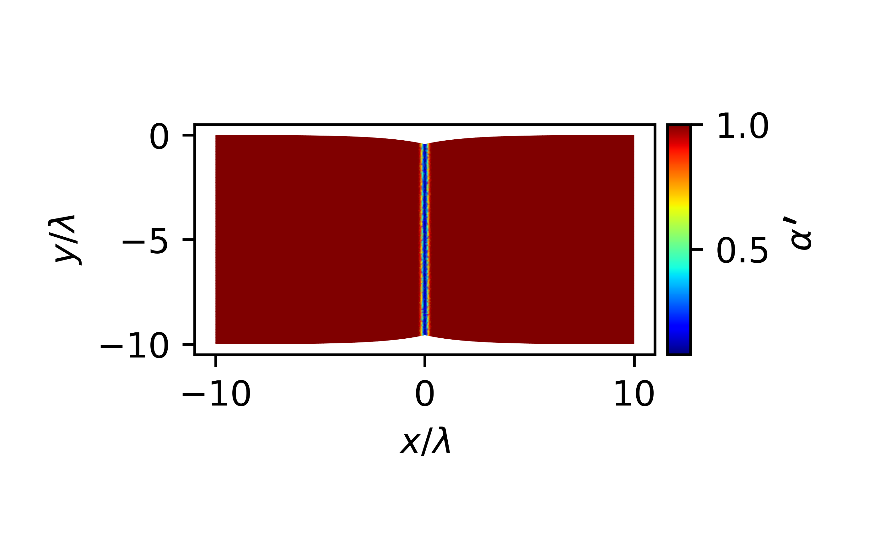
In addition to stoichiometry, previous work suggests that strain effects in the neighborhood of a grain boundary can also effect local superconducting properties. For example, a 1% strain can result in a 10% reduction in the Fermi level density of statesGodeke et al. 2018. In contrast, an excess of 5% Sn can result is more than a 50% reduction in the density of states at the Fermi level. Here, we focus on the dominant, stoichiometry effect and model a reduction in that is strongly localized to the grain boundary.
The Ginzburg-Landau parameter for Nb3Sn is 26, which is challenging to simulate because of the extreme separation in length scales that require a very refined mesh. However, the relevant physics for vortex nucleation are variations in material parameters on length scales comparable to the superconducting coherence length, . Therefore, we have simulated a moderate type-II material () but scaled the width of the segregated region (i.e., depleted ) so that its dimensions relative to are the same as that observed in Figure 3. At sufficiently high fields, the line of vortices undergoes a buckling instability when the vortex-vortex repulsion overcomes the pinning strength of the grain boundary. Because our simulations use a smaller value of the penetration depth, we under-estimate the vortex-vortex repulsion and overestimate the critical field at which the chain becomes unstable. However, the pinning force in real-world cavities also depends on details, such as the slope of the in the transition region, as we discuss below. These details will affect quantitative predictions for real-world cavities; however, we expect these simulations to capture the qualitative picture.
IV.2 Vortex Nucleation in Grain Boundaries
To simulate the nucleation of vortices into a grain boundary, we set the value of the magnetic field at the top and bottom boundary such that it is low enough that an array of vortices do not penetrate directly into the bulk, but large enough for vortices to enter into the grain boundaryPack et al. 2019. As we evolve in time (assuming a constant applied field), two different behaviors are observed depending on the magnitude of the applied field. In the first scenario, vortices enter into the grain boundary at the geometric divot. With increasing field, the spacing between vortices decreases until it reaches critical levels. In the second scenario, vortices first fill the grain boundary, as in the first case, but then begin to penetrate into the grain from the boundary.
Once a vortex has penetrated into the grain boundary, it is pushed from the surface, allowing more vortices to come in after it. Once space is available, another vortex penetrates. This continues until the vortices have filled the grain boundary, i.e. an optimal spacing between the vortices inside grain boundary has been achieved. This is illustrated by the sequence in Figure 9. Note that vortices are manifest as regions in which the order parameter is reduced to near zero at their center and exponentially decay radially outward to unity.


If the applied magnetic field is sufficiently high, vortices will also begin to penetrate into the bulk once the grain boundary has been filled. See, for example, the bottom of Figure 9. The escape of vortices into the bulk occurs through a buckling transition similar to that observed in anisotropic, layered superconductorsDodgson 2002. The field at which vortices penetrate from the grain boundary into the grain is dependent on the distribution of . The shallower the slope of the lower the applied field needs to be to nucleate vortices into the grain from the grain boundary. These results are summarized in the phase diagram in Figure 10. Comparing with results from section III, for a segregated region with in a cavity operating at (), we observe a non-trivial region of the phase diagram that admits flux trapped at the grain boundary.
The value of the applied field at which the vortices first leave the grain boundary and penetrate the bulk depends on the properties in the transition zone between the segregated and non-segregated region. If the transition form (segregated region) to (non-segregated region) is very sharp (as the blue solid curve in Figure 11), then vortices will be trapped in the grain boundary for larger fields. However, if the transition is more gradual (such as the orange dashed curve), then it is easier for vortices to escape the boundary and penetrate the bulk. Figures [8, 9, 10] were generated with a very sharp interface.

V Estimates of vortex dissipation at grain boundaries
Inhomogeneous properties of superconductors have high impact on the performance of SRF cavities, affecting figures of merit such as the residual resistance due to trapped magnetic flux Gurevich and Ciovati 2013; Hall et al. 2018; Liarte et al. 2018, and the superheating field Kramer 1968b; Catelani and Sethna 2008; Transtrum et al. 2011; Liarte et al. 2016; Liarte et al. 2017; Ngampruetikorn and Sauls 2019. Grain boundaries well aligned with the surface magnetic field can become weak spots for the nucleation of superconducting vortices (see Fig. 12), and could be ultimately responsible for the quench of an SRF cavity. Note that our Ginzburg-Landau model did not simulate the full semi-loops of Figure 12. In this section, we discuss simple estimates for the power dissipation and heat diffusion due to nucleation of vortices at grain boundaries in Nb3Sn cavities.

We start with an estimate for the power dissipated in an SRF cavity when a grain boundary is filled with superconducting vortices. We assume of order vortex lines are annihilated once per cycle, their energy is lost, and the power dissipated per vortex line is simply the drop in the energy of the outside magnetic field times the RF frequency. Our estimate gives a rough estimate for the actual power dissipated by vortices at grain boundaries, if the field reaches high enough values for them to enter.
The drop in magnetic energy when a vortex line of length nucleates into the superconductor is given by:
| (6) |
where is the volume, is the permeability of free space, is the fluxoid quantum, and is the penetration depth. Note that is also approximately the work done by the external magnetic field to push a vortex into the bulk of the superconductor: , where is the Lorentz force per length. Thus, our calculation gives the vortex dissipation at grain boundaries assuming that the vortices do not leave the grain boundary as the external field drops and changes sign, as our simulations indicate, and as one would expect for vortices that enter a distance more than , past the surface nucleation barrier. The total energy drop for a grain boundary of linear size with vortices spaced by (see Fig. 12) is , and the power dissipated per grain boundary is given by
| (7) |
where is the cavity frequency. For a 1.3GHz Nb3Sn cavity with typical grain size of m, we find nW at mT.
Note that our estimate relies on the assumption that vortices quickly fill the grain boundary before being annihilated during the RF cycle. If the vortex line relaxes slowly, the RF field might vanish and change sign before vortices had time to fill the grain boundary, and our assumption would not be valid. We now show that that is not the case — vortices move at extremely high speeds in the typical environment of Nb3Sn SRF cavities.
Consider the one-dimensional motion of a “train” of vortices moving through a grain boundary towards the superconductor interior (see Fig. 13). Assuming over-damped dynamics, the equations of motion for each vortex line of velocity read:
where is the Lorentz force per length at the surface, is the surface magnetic field, is the Bardeen-Stephen viscosity Bardeen and Stephen 1965, is the resistivity of the normal state and is the repulsion force from vortex into vortex . Thus,
| (8) |
For Nb3Sn at mT, we find m/ns and m/ns for ten vortices and one vortex, respectively. The average velocity of the vortex train is high enough for vortices to quickly fill in the grain boundary during the RF cycle, but this numerical value should be taken with a grain of salt. The Bardeen-Stephen formula is not valid at these high speeds, which also exceed the pair-breaking limit of the superconducting condensate Embon et al. 2017. In principle, one could incorporate pair-breaking mechanisms into our simple estimates by using the nonlinear viscosity calculated by Larkin and Ovchinnikov (LO) Larkin and Ovchinnikov 1975: , where is the Bardeen-Stephen viscosity and the LO velocity marks the onset of highly dissipative states for straight vortices. Following the same steps that we have used to calculate , and assuming that each vortex moves with the same vortex-train velocity , we find
| (9) |
for , showing that nonlinear corrections lead to an increase of the velocity of the vortex train from the Bardeen-Stephen result. However, note that estimates for Nb3Sn at low temperatures Gurevich and Ciovati 2008 yield km/s, which is much smaller than our estimates for , so that a more sophisticated analysis is needed to better describe vortex motion at these high-speed regimes. In recent work Pathirana and Gurevich 2020, Pathirana and Gurevich consider the nonlinear dynamics of curvilinear vortices subject to LO viscous forces to study dissipation and vortex teardown instabilities.
Grain boundary activation might be associated with the degradation of the quality factor of SRF cavities at high fields. We now use our estimates to calculate the number of active grain boundaries needed to deplete by a certain amount.
The quality factor is given by , where is the dissipated power per unit area and is a geometry factor. We break up the total surface area of the cavity into blocks, so that , where is the average area occupied by one grain boundary. Assume inactive and active blocks dissipate power and , respectively, where by active block we mean a block with a grain boundary filled with vortices. For active blocks,
| (10) |
where is the ratio of active grain boundaries. In the absence of active grain boundaries, we assume is constant (i.e. ), so that
| (11) |
Plugging Eq. (11) into Eq. (10) and solving for , we find
| (12) |
To estimate the percentage of active grain boundaries that is needed for to drop by a certain amount, we assume Q is constant and equal to for fields up to mT, and then decreases exponentially until it reaches at mT. This form for the -slope profile is shown in yellow in Fig. 14, and is chosen to roughly mimic the experimental data shown with red symbols in Figure 1. Here we assume that degradation is solely due to grain activation; the field of vortex penetration is chosen to roughly match that of the onset of the experimental Q slope (mT). Note that Calculations for the exactly solvable limit of Josephson vortices which penetrate along weakly-coupled planar junctions yield a threshold critical current density , where is the Josephson penetration depth, which is assumed to be much larger than the penetration depth Sheikhzada and Gurevich 2017. Figure 14 shows a plot of the percentage of active grain boundaries (, blue curve) as a function of corresponding to the artificial -slope profile shown in the yellow curve (using Nb3Sn parameters with , m2 and ). Note that about 0.03% of the surface grain boundaries need be filled with vortices for to drop from to for Nb3Sn at about 66mT.
We end this section with a simple model calculation of the steady-state thermal heating at a grain boundary. Figure 15 illustrates our model for thermal diffusion near an active grain boundary. Cross sections of Nb and Nb3Sn layers are illustrated below and above the yellow dashed line in Fig. 15, respectively. The Nb surface is in contact with a low-temperature He bath. The Nb3Sn surface is in contact with vacuum, and is subject to a parallel oscillating magnetic field. The grain boundary is represented by a red rectangle at the top center of Figure 15, and has linear size . White arrows depict approximate directions for heat diffusion in our model. First, we assume one-dimensional heat diffusion away from the grain boundary up to a distance . We expect the heat front to attain a semi-spherical shape for distances . We then assume three-dimensional heat diffusion away from a half-sphere of radius for distances . For we consider the Nb3Sn thermal conductivity . At last, we assume three-dimensional heat diffusion away from a half-sphere of radius for distances , with given by the Nb thermal conductivity . Note that our assumptions are stronger when ( for typical Nb3Sn/Nb SRF cavities).
The equilibrium temperature profile can then be cast from the stationary solutions of the heat equation in each region:
| (13) |
where , , and are constants, and is the stationary solution of the one-dimensional heat equation (the Nb3Sn thermal conductivity strongly varies with temperature in this region Cody and Cohen 1964, which complicates the problem of finding an analytical solution for ) 11 1 Note that the temperature dependence of the thermal conductivity of Nb3Sn should also change the stationary solution of the three-dimensional heat equation for . Here we ignore this effect for the sake of mathematical simplicity, since our qualitative conclusions are not altered if we incorporate the temperature dependence of in this region.. Note that we relax the definition of the coordinate here, which should be interpreted as a lateral distance away from the grain boundary for , and a depth coordinate towards the Helium bath for distances .
To calculate , we use Fourier’s law — , where is the heat flux. The stationary solution of the heat equation can be found from the solution of , i.e.
| (14) |
where is constant.
The thermal conductivity in the superconducting layer has two important contributions: a phonon contribution and an electronic component (carried by superconducting quasiparticles). The low-temperature phonon thermal conductivity is strongly dependent on the morphology of the crystal Cahill and Pohl 1988; in clean insulating crystals it is dominated by scattering off grain boundaries and sample boundaries, and varies as . Scattering off impurities can cut off the contribution of high-frequency phonons, or even resonantly cut off certain frequency bands. All of these mechanisms lead to a thermal conductivity that monotonically increases with temperature, so we avoid the complexity by using a constant phonon thermal conductivity , giving a lower bound for the conductivity and hence an upper limit to the heating. The electronic portion of the thermal conductivity in the normal metal at low temperatures is roughly independent of temperature, and is set by the electronic mean-free path. In the superconductor, it decreases exponentially as , as seen experimentally Cody and Cohen 1964. Using the BCS relation between the gap and the transition temperature, we therefore use
| (15) |
We use the normal electron thermal conductivity W/mK from Cody and Cohen 1964. Because the electronic contribution is negligible at the operating temperature of the cavity, we set W/mK as the approximate total thermal conductivity of Nb3Sn at 2K Cody and Cohen 1964. Both of these constants are dependent upon the preparation of the film, and also could vary from one region of the film to another as the growth conditions or the underlying Nb grain orientations vary.
Integration of Eq. (14) results in
| (16) |
where is constant, and
| (17) |
with denoting the exponential integral function. is then the solution of Eq. (16) for . Note that our simple model assumes that the quasiparticles and the phonons remain at the same effective temperature (the inelastic electronic mean free path is small), and that both remain diffusive (the elastic phonon and electron mean free paths are small). Violating either of these assumptions would likely lower the transport of energy away from the grain boundary, making the heating more dangerous.
We focus our attention on grain-boundary activation and ignore other sources of power dissipation. These sources, in particular the BCS dissipation that exponentially increases with temperature, may have a significant impact on stationary temperature profiles, with possible indicatives of thermal runaway and cavity quenches at low fields. As we discuss at the end of this section, our simple estimates suggest that larger grain boundaries or multiple nearby boundaries could already raise the temperature high enough to quench the cavity. Hence, although the inclusion of other sources would lead to a more accurate description of heat diffusion near active grain boundaries, they will not lead to qualitative changes in our conclusions. Thus, we assume that the heat flux is the power dissipated per grain boundary () per unit area. We use Fourier’s law to determine the coefficients , and in Eqs. (13) and (16). For , , so that:
| (18) |
For (), , () and (), so that:
| (19) |
To find , we use , where is the temperature of the Helium bath:
| (20) |
To find and , we use the continuity of at and , respectively (we ignore the Kapitza resistance at the interface between Nb3Sn and Nb). Thus,
| (21) |
and
| (22) |
Figure 16 shows temperature profiles (Eq. (13)) near an active grain boundary for Nb3Sn/Nb systems at mT. Note that the temperature of an active grain boundary increases to about 10K near the boundary surface for a Helium temperature of 2K. Although this increase in temperature is not large enough to drive Nb3Sn into the normal state, it certainly has significant impact on the superconducting properties. Also, note that the temperature decays to nearly as approaches twice the grain size , suggesting that heating due to grain-boundary activation is mostly localized.
A temperature rise of 10K at the grain boundary is over half of the critical temperature of the film, suggesting that larger grain boundaries or multiple nearby boundaries could raise the temperature high enough to quench the cavity. Cavities with tin-rich grain boundaries and more pristine grain boundaries show the same quench fields, suggesting that another mechanism controls the quench fields of existing Nb3Sn cavities. If the excess dissipation in the cavities with tin-rich boundaries is due to vortex penetration (Fig. 14), one would expect rare events with large or multiple grain boundaries would happen, suggesting that our grain-boundary heating estimate is unduly pessimistic. Alternatively, it remains possible that the grain boundaries have high superheating fields, and the excess dissipation has another explanation. In any case, our estimates suggest that vortex entry at grain boundaries should be expected for tin-rich boundaries well below the superheating field for a perfect crystal, and that the subsequent heat release should be important both as a contribution to the overall dissipation and as a quench mechanism for the cavity.
VI Conclusion
In this work we have presented an interdisciplinary, multi-scale study of vortex nucleation in Sn-segregated grain boundaries and its subsequent effect on SRF performance. Scanning transmission electron microscopy images and energy dispersive spectroscopy show Sn concentration as high as 35 at.% and widths 3nm in chemical composition in grain boundaries. We used density functional theory to estimate the effective critical temperature for the material in the segregation zone and find that the effective can be reduced to as low as 5 K for Sn concentrations in excess of 30 at.%. Next, we used these calculations as inputs into time-dependent Ginzburg-Landau simulations. These simulations demonstrate that grain boundaries can act as nucleation sites for magnetic vortices. The grain boundaries then act as pinning “planes” after nucleation that allow vortices to move vertically along the grain boundary, but prevent them from moving laterally into the bulk. We have seen that for a range of applied fields, vortices may nucleate at but remain constrained to the grain boundary. These vortices will nucleate and annihilate once per RF cycle, and we estimate the superconducting losses of this phenomenon at the scale of SRF cavities. We have shown that as long as vortices do not penetrate the bulk grain, losses are localized near the grain boundary and will not lead to a global quench. However, the annihilation process each cycle will lead to a reduction in the quality factor that increases with larger applied fields, consistent with the experimentally observed Q-slope.
SRF cavities are an important application area that require multi-disciplinary talents to address. This study has leveraged the skills of accelerator physicists, material scientists, and condensed matter theorists with expertise across a range of scales to explore a question fundamental to the advancement of next-generation SRF material, Nb3Sn. This study has presented evidence that segregation zones in grain boundaries play an important role in cavity performance. Understanding the mechanism behind the Q-slope will motivate new manufacturing protocols and help constrain the design space of future cavities.
VII Acknowledgement
We would like to thank Matthias Liepe, and Richard Hennig for helpful conversations. This research is supported by the United States Department of Energy, Offices of High Energy. Fermilab is operated by the Fermi Research Alliance LLC under Contract No. DE-AC02-07CH11359 with the United States Department of Energy. This work made use of the EPIC, Keck-II, and/or SPID facilities of Northwestern University’s NUANCE Center, which received support from the Soft and Hybrid Nanotechnology Experimental (SHyNE) Resource (NSF ECCS-1542205); the MRSEC program (NSF DMR-1121262) at the Materials Research Center; the International Institute for Nanotechnology (IIN); the Keck Foundation; and the State of Illinois, through the IIN. This work was supported by the US National Science Foundation under Award OIA-1549132, the Center for Bright Beams.
References
- Liarte et al. (2017) D. B. Liarte, S. Posen, M. K. Transtrum, G. Catelani, M. Liepe, and J. P. Sethna, Superconductor Science and Technology 30, 033002 (2017).
- Transtrum et al. (2011) M. K. Transtrum, G. Catelani, and J. P. Sethna, Physical Review B 83, 094505 (2011).
- Chapman (1995) S. J. Chapman, SIAM Journal on Applied Mathematics 55, 1233 (1995).
- Dolgert et al. (1996) A. J. Dolgert, S. J. Di Bartolo, and A. T. Dorsey, Physical Review B 53, 5650 (1996).
- Kramer (1968a) L. Kramer, Physical Review 170, 475 (1968a).
- Posen et al. (2015) S. Posen, N. Valles, and M. Liepe, Physical review letters 115, 047001 (2015).
- Catelani and Sethna (2008) G. Catelani and J. P. Sethna, Physical Review B 78, 224509 (2008).
- Lin and Gurevich (2012) F. P.-J. Lin and A. Gurevich, Physical Review B 85, 054513 (2012).
- Pack et al. (2019) A. R. Pack, J. Carlson, S. Wadsworth, and M. K. Transtrum, arXiv preprint arXiv:1911.02132 (2019).
- Aladyshkin et al. (2001) A. Y. Aladyshkin, A. Mel’Nikov, I. Shereshevsky, and I. Tokman, Physica C: Superconductivity 361, 67 (2001).
- Burlachkov et al. (1991) L. Burlachkov, M. Konczykowski, Y. Yeshurun, and F. Holtzberg, Journal of applied physics 70, 5759 (1991).
- Vodolazov (2000) D. Y. Vodolazov, Physical Review B 62, 8691 (2000).
- Soininen and Kopnin (1994) P. Soininen and N. Kopnin, Physical Review B 49, 12087 (1994).
- Scanlan et al. (1975) R. Scanlan, W. Fietz, and E. Koch, Journal of Applied Physics 46, 2244 (1975).
- Godeke (2006) A. Godeke, Superconductor Science and Technology 19, R68 (2006).
- Suenaga and Jansen (1983) M. Suenaga and W. Jansen, Applied physics letters 43, 791 (1983).
- Sandim et al. (2013) M. Sandim, D. Tytko, A. Kostka, P. Choi, S. Awaji, K. Watanabe, and D. Raabe, Superconductor Science and Technology 26, 055008 (2013).
- Posen and Hall (2017) S. Posen and D. L. Hall, Superconductor Science and Technology 30, 033004 (2017).
- Posen and Liepe (2014) S. Posen and M. Liepe, Physical Review Special Topics-Accelerators and Beams 17, 112001 (2014).
- Posen et al. (2019) S. Posen, J. Lee, O. Melnychuk, Y. Pischalnikov, D. Seidman, D. Sergatskov, and B. Tennis, in 19th Int. Conf. on RF Superconductivity (SRF’19), Dresden, Germany, 30 June-05 July 2019 (JACOW Publishing, Geneva, Switzerland, 2019) pp. 818–822.
- Müller et al. (2000) G. Müller, H. Piel, J. Pouryamout, P. Boccard, and P. Kneisel, in Proceedings of the Workshop on Thin Film Coating Methods for Superconducting Accelerating Cavities (2000).
- Gurevich (2017) A. Gurevich, Superconductor Science and Technology 30, 034004 (2017).
- Hall (2017) D. L. Hall, New Insights into the Limitations on the Efficiency and AchievableGradients in Nb 3 Sn SRF Cavities (Cornell University, 2017).
- Lee et al. (2018) J. Lee, S. Posen, Z. Mao, Y. Trenikhina, K. He, D. L. Hall, M. Liepe, and D. N. Seidman, Superconductor Science and Technology 32, 024001 (2018).
- Trenikhina et al. (2017) Y. Trenikhina, S. Posen, A. Romanenko, M. Sardela, J.-M. Zuo, D. Hall, and M. Liepe, Superconductor Science and Technology 31, 015004 (2017).
- Becker et al. (2015) C. Becker, S. Posen, N. Groll, R. Cook, C. M. Schlepütz, D. L. Hall, M. Liepe, M. Pellin, J. Zasadzinski, and T. Proslier, Applied Physics Letters 106, 082602 (2015).
- Lee et al. (2020) J. Lee, Z. Mao, K. He, Z. H. Sung, T. Spina, S.-I. Baik, D. L. Hall, M. Liepe, D. N. Seidman, and S. Posen, Acta Materialia 188, 155 (2020).
- Dillon et al. (2007) S. J. Dillon, M. Tang, W. C. Carter, and M. P. Harmer, Acta Materialia 55, 6208 (2007).
- Seidman (2002) D. N. Seidman, Annual Review of Materials Research 32, 235 (2002).
- Rittner et al. (1997) J. Rittner, D. Udler, and D. Seidman, Interface Science 4, 65 (1997).
- Kelley et al. (2020) M. M. Kelley, N. S. Sitaraman, and T. A. Arias, arXiv preprint arXiv:2005.12133 (2020).
- Kempshall et al. (2002) B. Kempshall, B. Prenitzer, and L. Giannuzzi, Scripta materialia 47, 447 (2002).
- Sitaraman et al. (2019) N. S. Sitaraman, J. Carlson, A. R. Pack, R. D. Porter, M. U. Liepe, M. K. Transtrum, and T. A. Arias, arXiv preprint arXiv:1912.07576 (2019).
- Godeke et al. (2018) A. Godeke, F. Hellman, H. ten Kate, and M. Mentink, Superconductor Science and Technology 31, 105011 (2018).
- McMillan (1968) W. L. McMillan, Physical Review 167, 331 (1968).
- Sundararaman et al. (2017) R. Sundararaman, K. Letchworth-Weaver, K. A. Schwarz, D. Gunceler, O. Y., and T. A. Arias, SoftwareX 6, 278 (2017).
- Marzari and Vanderbilt (1997) N. Marzari and D. Vanderbilt, Physical Review B 56, 12847 (1997).
- Devantay et al. (1981) H. Devantay, J. L. Jorda, M. Decroux, J. Muller, and R. Flükiger, Materials Science 16, 2145–2153 (1981).
- Alnæs et al. (2015) M. S. Alnæs, J. Blechta, J. Hake, A. Johansson, B. Kehlet, A. Logg, C. Richardson, J. Ring, M. E. Rognes, and G. N. Wells, Archive of Numerical Software 3 (2015), 10.11588/ans.2015.100.20553.
- Logg et al. (2012) A. Logg, K.-A. Mardal, and G. Wells, Automated solution of differential equations by the finite element method: The FEniCS book, Vol. 84 (Springer Science & Business Media, 2012).
- Gao and Sun (2015) H. Gao and W. Sun, Journal of Computational Physics 294, 329 (2015).
- Kramer and Watts-Tobin (1978) L. Kramer and R. Watts-Tobin, Physical Review Letters 40, 1041 (1978).
- Dodgson (2002) M. J. Dodgson, Physical Review B 66, 014509 (2002).
- Gurevich and Ciovati (2013) A. Gurevich and G. Ciovati, Phys. Rev. B 87, 054502 (2013).
- Hall et al. (2018) D. Hall, D. Liarte, M. Liepe, R. Porter, and J. Sethna, in Proc. of International Conference on RF Superconductivity (SRF’17), Lanzhou, China, July 17-21, 2017, International Conference on RF Superconductivity No. 18 (JACoW, Geneva, Switzerland, 2018) pp. 844–847, https://doi.org/10.18429/JACoW-SRF2017-THPB042.
- Liarte et al. (2018) D. B. Liarte, D. Hall, P. N. Koufalis, A. Miyazaki, A. Senanian, M. Liepe, and J. P. Sethna, Phys. Rev. Applied 10, 054057 (2018).
- Kramer (1968b) L. Kramer, Phys. Rev. 170, 475 (1968b).
- Liarte et al. (2016) D. B. Liarte, M. K. Transtrum, and J. P. Sethna, Phys. Rev. B 94, 144504 (2016).
- Ngampruetikorn and Sauls (2019) V. Ngampruetikorn and J. A. Sauls, Phys. Rev. Research 1, 012015 (2019).
- Bardeen and Stephen (1965) J. Bardeen and M. J. Stephen, Phys. Rev. 140, A1197 (1965).
- Embon et al. (2017) L. Embon, Y. Anahory, Ž. L. Jelić, E. O. Lachman, Y. Myasoedov, M. E. Huber, G. P. Mikitik, A. V. Silhanek, M. V. Milošević, A. Gurevich, et al., Nature communications 8, 85 (2017).
- Larkin and Ovchinnikov (1975) A. Larkin and Y. Ovchinnikov, Sov. Phys. JETP 41, 960 (1975).
- Gurevich and Ciovati (2008) A. Gurevich and G. Ciovati, Phys. Rev. B 77, 104501 (2008).
- Pathirana and Gurevich (2020) W. P. M. R. Pathirana and A. Gurevich, Phys. Rev. B 101, 064504 (2020).
- Sheikhzada and Gurevich (2017) A. Sheikhzada and A. Gurevich, Phys. Rev. B 95, 214507 (2017).
- Cody and Cohen (1964) G. D. Cody and R. W. Cohen, Rev. Mod. Phys. 36, 121 (1964).
- (57) Note that the temperature dependence of the thermal conductivity of Nb3Sn should also change the stationary solution of the three-dimensional heat equation for . Here we ignore this effect for the sake of mathematical simplicity, since our qualitative conclusions are not altered if we incorporate the temperature dependence of in this region.
- Cahill and Pohl (1988) D. G. Cahill and R. O. Pohl, Annual Review of Physical Chemistry 39, 93 (1988), https://doi.org/10.1146/annurev.pc.39.100188.000521 .