Snitch: A tiny Pseudo Dual-Issue Processor for Area and Energy Efficient Execution of Floating-Point Intensive WorkloadsPubID: pubid: 0018-9340 ©2020 IEEE
Abstract
Data-parallel applications, such as data analytics, machine learning, and scientific computing, are placing an ever-growing demand on floating-point operations per second on emerging systems. With increasing integration density, the quest for energy efficiency becomes the number one design concern. While dedicated accelerators provide high energy efficiency, they are over-specialized and hard to adjust to algorithmic changes. We propose an architectural concept that tackles the issues of achieving extreme energy efficiency while still maintaining high flexibility as a general-purpose compute engine. The key idea is to pair a tiny (kilo gate equivalent) control core, called Snitch, with a double-precision floating-point unit (FPU) to adjust the compute to control ratio. While traditionally minimizing non-floating-point unit (FPU) area and achieving high floating-point utilization has been a trade-off, with Snitch, we achieve them both, by enhancing the ISA with two minimally intrusive extensions: stream semantic registers (SSR) and a floating-point repetition instruction (FREP). SSRs allow the core to implicitly encode load/store instructions as register reads/writes, eliding many explicit memory instructions. The FREP extension decouples the floating-point and integer pipeline by sequencing instructions from a micro-loop buffer. These ISA extensions significantly reduce the pressure on the core and free it up for other tasks, making Snitch and FPU effectively dual-issue at a minimal incremental cost of 3.2%. The two low overhead ISA extensions make Snitch more flexible than a contemporary vector processor lane, achieving a energy-efficiency improvement. We have evaluated the proposed core and ISA extensions on an octa-core cluster in 22 nm technology. We achieve more than multi-core speed-up and a gain in energy efficiency on several parallel microkernels.
Index Terms:
RISC-V, many-core, energy efficiency, general purposeI Introduction
The ever-increasing demand for floating-point performance in scientific computing, machine learning, big data analytics, and human-computer interaction are dominating the requirements for next-generation computer systems [1]. The paramount design goal to satisfy the demand of computing resources is energy efficiency: Shrinking feature sizes allow us to pack billions of transistors in dies as large as . The high transistor density makes it impossible to switch all of them at the same time at high speed as the consumed power in the form of heat cannot dissipate into the environment fast enough. Ultimately, designers have to be more careful than ever only to spend energy on logic, which contributes to solving the problem.
Thus, we see an explosion on the number of accelerators solely dedicated to solving one particular problem efficiently. Unfortunately, there is only a limited optimization space that, with the end of technology scaling, will reach a limit of a near-optimal hardware architecture for a certain problem [2]. Furthermore, algorithms can evolve rapidly, thereby making domain-specific architectures less efficient for such algorithms [3]. On the other end of the spectrum, we can find fully programmable systems such as graphics processing units (GPUs) and even more general-purpose units like central processing units (CPUs). The programmability and flexibility of those systems incur significant overhead and make such systems less energy efficient. Furthermore, CPUs and GPUs (to a lesser degree) are affected by the Von Neumann bottleneck: The rate of which information can travel from data and instruction memory limits the computational throughput of the architecture. More hardware is necessary to mitigate these effects, such as caching, multi-threading, and super-scalar out-of-order processor pipelines [4]. All these mitigation techniques aim to increase the utilization of the compute resource, in this case, the FPU. They achieve this goal at a price of much-increased hardware complexity, which in turn decreases efficiency because a smaller part of the silicon budget remains dedicated to compute units. A reproducible example, thanks due to its open-source nature, is the out-of-order BOOM CPU [5, 6]: Approximately of the core’s overall area, is spent on the FPU.11 1 estimated on a post-synthesis netlist in Globalfoundries 22 nm FDX More advanced CPUs such as AMD’s Zen2 architecture show a better compute per area efficiency (around ), primarily thanks to the wide single instruction multiple data (SIMD) floating-point execution units [7].
I-A Design Goal: Area and Energy efficiency

To give the reader quantitative intuition on the severe efficiency limits affecting programmable architectures, let us consider, the simple kernel of a dot product () in Figure 1(b,c). The corresponding energies per instruction type in Figure 1(a) for a 64-bit application-class RISC-V processor as reported in [8] in a technology. The kernel consists of up of five instructions. Four of those instructions perform bookkeeping tasks such as moving the data into the local register file (RF) on which arithmetic instructions can operate and looping over all elements of the input vectors. In total, the energy used for performing an element multiplication and addition in this setting is . The only “useful” workload in this kernel is performed by the FPU, which accounts for . The rest of the energy () is spent on auxiliary tasks. Even this short kernel gives us an immediate intuition on where energy efficiency is lost. FPU utilization is low (), mostly due to load and store and loop management instructions.
I-B Existing Mitigation Techniques and Architectures
Techniques and architectures exist that try to mitigate the efficiency issue highlighted above.
- •
Instruction set architecture (ISA) extensions: Post increment load and store instruction can accelerate pointer bumping within a loop [9]. For an efficient implementation they require a second write-port into the RF, therefore increasing the implementation cost. SIMD such as Streaming SIMD extensions (SSE)/advanced vector extensions (AVX) [10] in x86 or NEON Media Processing Engine (NEON) [11] in Advanced RISC Machines (Arm) perform a single-instruction on a fixed amount of data items in a parallel fashion. Therefore reducing the total loop count and amortizing the loop overhead per computation. Wide SIMD data-paths are quite inflexible when elements need to be accessed individually: Dedicated shuffle operations are used to bring the data into a SIMD-amenable form.
- •
- •
GPUs: Single instruction multiple thread (SIMT) architectures such as NVIDIA’s V100 [15] GPU use multiple parallel scalar threads that execute the same instructions. Hardware scheduling of threads hides memory latency. Coalescing units bundle the memory traffic to make accesses into (main) memory more efficient. However, the hardware to manage threads is quite complex and comes at a cost that offsets the energy efficiency of GPUs. The thread scheduler needs to swap different thread contexts on the same streaming multiprocessor (SM) whenever it detects a stalling thread (group) waiting for memory loads to return or due to different outcomes of branches (branch divergence). This means that the SM must keep a very large number of thread contexts (including the relatively large RF) in local static random-access memories (SRAMs) [16]. SRAM accesses incur a higher energy cost than reads to flipflop-based memories and enforce a word-wise access granularity. For GPUs to overcome these limitations, they offer operand caches in which software can cache operands and results, which are then reusable at a later point in time, which decreases area and energy efficiency. For example, NVIDIA’s Volta architecture offers two 64-bit read ports on its register file per thread. To sustain a three operand fused multiply-add (FMA) instruction, it needs to source one operand from one of its operand caches [16].
I-C Contributions
The solutions we propose here to solve the problems outlined above are the following:
- 1.
A general-purpose, single-stage, single-issue core, called Snitch, tuned for high energy efficiency. Aiming to maximize the compute/control ratio (making the FPU the dominant part of the design) mitigating the effects of deep pipelines and dynamic scheduling.
- 2.
An ISA extension, originally proposed by Schuiki et al. [17], called stream semantic register (SSR). This extension accelerates data-oblivious [18] problems by providing an efficient semantic to read and write from memory. Load and store instructions which follow affine access patterns (streams) are implicitly mapped to register read/writes. SSRs effectively elide all explicit memory operations. Semantically they are comparable to vector operations as they operate on vectors (tensors) without the explicit need for load and store instructions. We have enhanced the SSR implementation by providing shadow registers to overlap configuration and computation. The shadow registers are transparent from a programming perspective, new configurations are accepted as long as the shadow registers are not full. As soon as the current configuration has finished, the shadow register’s value is swapped in as a new active configuration. The streamers immediately start fetching using the new stream configuration.
- 3.
A second ISA extension, floating-point repetition instruction (FREP), which controls an FPU sequence Buffer. The FPU and the integer core in the proposed system are fully decoupled and only synchronize with explicit move instructions between the two subsystems. The FPU sequencer is situated on the offloading path of the integer core to the FPU. It provides a small, configurable size sequence buffer from which it can sequence floating-point instructions in a configurable manner. The sequence buffer frees the integer core from issuing instructions to the FPU that is, therefore, available for other control tasks. This makes this single-issue, in-order core pseudo dual-issue, enabling it to overlap independent integer and floating-point instructions. Furthermore, the sequence buffer eliminates the need for loops in the code and reduces the pressure on the instruction fetch. Repetition instructions are also implemented in the X86 [19] and TMS320C28x digital signal processor (DSP) [20] ISAs. Compared to those instructions that allow only a single instruction to be repeated, our approach, in conjunction with SSRs, offers greater flexibility as a few instruction can program the entire loop-buffer, and complex operations can be entirely offloaded.
While traditionally minimizing non-FPU area and achieving floating-point high utilization has been a trade-off, we can eliminate the need to compromise: Our extensions have negligible area cost and boost FPU utilization significantly. Our Snitch core achieves the same clock frequency, higher flexibility, and is more area- and energy-efficient than a conventional vector processor lane.
From the design and implementation viewpoint, the contributions of this work are:
- 1.
A fully programmable, shared memory, multi-core system tuned for utmost energy efficiency by using a tiny integer core attached to a double-precision FPU. Achieving more energy efficiency and better FPU utilization on small matrices than the current state of the art.
- 2.
An implementation of the SSR [17] enhanced with shadow registers to allow overlapping loop-setup with ongoing operations using the FREP extension enabling the usage of our SSR and FREP extensions on more irregular kernels such as Fast Fourier Transform (FFT). Achieving speed-ups of in the single-core case and close to in the parallel octa-core case for the FFT benchmark.
- 3.
A decoupled FPU and integer core architecture featuring a sequence buffer that can independently service the FPU while the integer core is busy with control tasks. This extension, together with the SSR, make the small integer core pseudo dual-issue at a minimal incremental area cost of less than for the core complex and on the cluster level including memories.
The rest of the paper is organized as follows: Section II describes the proposed architecture and ISA extensions, Section III offers more details on the programming model of the system and the ISA extensions, Section IV presents the experimental setup, evaluation and comparison to other systems. The last sections conclude the presented work and present future research directions.
II Architecture

Figure 2 depicts the microarchitecture of the proposed system. The smallest unit of repetition is a Snitch CC. It contains the integer core and the FPU subsystem. The core is repeated times to form a Snitch Hive. Cores of a Hive share an integer multiply/divide unit and an L1 instruction cache. Hives make up a Snitch Cluster that shares a TCDM acting as a software-managed L1 cache. clusters share last level memory via a crossbar. All the parameters can be freely adjusted. For example, a Hive can just contain one core, therefore effectively making it a private multiplier and instruction cache. Similarly, a cluster can just contain one Hive with one core, making the TCDM a private scratchpad memory.
II-A Snitch Core Complex
The smallest unit of repetition is a Snitch CC, see Figure 2 (4). It contains an RV32IMAFD (RV32G) RISC-V core and can be configured with or without support for the proposed ISA extensions. Depending on the technology and desired speed targets of the design, the offloading request, response, and the load/store interface to the TCDM can be fully decoupled, increasing the design’s clock frequency at the expense of increased latency of one cycle.
II-A1 Integer Core
The foundation of the system is an ultra-small (), and energy-efficient 32 bit integer RISC-V compute unit, which we call Snitch (Figure 2 (1)). Snitch implements the entire (mandatory) integer base (RV32I). As its RF dominates the design of the CPU implementation, we alternatively also support the embedded profile (E) as the other implementation choice. The embedded profile only provides 15 integer registers instead of 31. In addition, the RF can either be implemented based on D-latches or D-flipflops. Each Snitch has a dedicated instruction fetch port, a data port with an independent valid-then-ready [21] decoupled request and response path, and a generic accelerator offloading interface. The accelerator interface has full support for offloading an entire 32 bit RISC-V instruction, and we re-use the same RISC-V instruction encoding. This saves energy in the core’s decoding logic as only a few bits need to be decoded to decide whether to offload an instruction or not. The interface has two independent decoupled channels. One for offloading an operation, up to three operands, and a back-channel for writing-back the result of the offloaded operation. In the presented design, we use the accelerator port to offload integer multiply/divide and floating-point instructions.
As our system’s workload focuses on floating-point computation Snitch was implemented with a minimal area footprint. The core is a single-stage, single-issue, in-order design. Integer instructions with all of their operands available (no data dependencies present) can be fetched, decoded, executed, and written back in the same cycle. We chose this design point to maximize energy efficiency and keep the design area at a minimum. The core keeps track of all 31 registers (the zero register is not writable, hence it does not need dedicated tracking) using a single bit in a scoreboard. There are three classes of instructions that need special handling:
Integer instructions
Most of the instructions contained in the RISC-V I subset, such as integer arithmetic instructions, manipulation of control and status registers (CSRs), and control flow changes, can be executed in a single-cycle as soon as all operands are available. Integer multiply/divide instructions are part of the M subset and are offloaded to the (possibly) shared multiply/divide unit. There is no source of stalling as the arithmetic logic unit (ALU) is fully combinational and executes its instruction in a single cycle. To foster the re-use of the ALU, it also performs comparison for branches, calculates CSR masks, and performs address calculations for load/store instructions.
Load/Store instructions
Load/store instructions execute as soon as all operands are available, and the memory subsystem can process a new request. The data port of the core can exert back-pressure onto the load/store subsystem. Furthermore, the load store unit (LSU) needs to keep track of issued load instructions and perform re-alignment and possible sign-extension. The core can have a configurable number of outstanding load instructions to the non-blocking memory hierarchy. Store instructions are considered fire-and-forget from a core perspective. The memory subsystem needs to maintain issue order as the core expects the arrival of load values in-order.
In addition to regular load and stores, the LSU can also issue atomic memory operations and load-reserved/store-conditional (LR/SC) as defined by the RISC-V atomic memory operation specification. From a core perspective, the only difference is that the core also sends an atomic operation to the memory subsystem alongside the address and data. We provide additional signaling to accomplish that.
Accelerator/special function unit instructions
Off-loaded instruction can execute as soon as all operands are available, and the accelerator interface can accept a new offloading request. We distinguish three types of instructions:
- 1.
Both destination and source operands are in the integer RF, such as integer multiplication and division. Snitch’s scoreboard keeps track of the destination operand.
- 2.
Source operands are in the integer RF, and the receiving unit maintains the destination register. Such an example would be a move from integer to floating-point RF.
- 3.
Both operands are outside of the integer RF, such as any floating-point compute instruction (e.g., FMA).
We offload floating-point instructions to the core-private FP-SS (Section II-A2). As most of the floating-point instructions operate on a separate floating-point RF we can easily decouple the floating-point logic from the integer logic. The RISC-V ISA specifies explicit move instructions from and to the floating-point RF, which makes this ISA particularly amenable for such an implementation. Decoupling the FP-SS from the integer core makes it possible to alter and sequence floating-point instructions into the FP-SS. This is discussed in detail in Section II-E.
The second compelling use-case of the accelerator interface is to share expensive but, in our case, uncommonly used resources [22]. We provide a hardware implementation of the multiplication and division instructions for RISC-V (M). This includes a fully pipelined 32 bit multiplier, and a 32 bit bit-serial integer divider with preliminary operand shifting for an early-out division — all cores of a Hive share such a hardware multiply/divide unit. Integer multiplications are two-cycle instructions while divisions are bit-serial and take up to 32 cycles in the worst case. By controlling the number of cores per Hive, the designer can adjust the sharing ratio. Sharing is independent of the functionality, and possibly many other resources can be shared, for example, a bit-manipulation ALU.
As the RF only contains a single write-port, the three sources mentioned above contend over the single write port in a priority arbitrated fashion. Single-cycle instructions have priority over results from the LSU over write-backs from the accelerator interface. That makes it possible to interleave results if an integer instruction does not need to write back, such as branch instructions, for example. Requests to the memory subsystem are only issued if there is space available to store the load result. Hence, cores cannot block each other with outstanding requests to the memory hierarchy. The integer core has priority on the register file to reduce the amount of logic necessary to retire a single-cycle instruction.
The Snitch integer core is formally verified against the ISA specification using the open-source RISC-V formal framework [23].
II-A2 FPU Subsystem
The FP-SS, see Figure 2 (2,3), bundles an IEEE-754 compliant FPU with a 3264 bit RF. The FP-SS has its own dedicated scoreboard where it keeps track of all registers in a similar fashion to the integer core. The FPU is parameterizable in supported precision and operation latency [24]. All floating-point operations are fully pipelined (with possibly different pipeline depths). Operations without dependencies can be issued back to back. In addition to the FPU it also contains a separate LSU dedicated to loading and storing floating-point data from/to the floating-point RF, the address calculation is performed in the integer core, which significantly reduces the area of the LSU. Furthermore, the FP-SS contains two SSRs which map, upon activation through a CSR write, registers ft0 and ft1 to memory streams. The architecture of the streamers is depicted in Figure 3 and described in more detail in Section II-D.
II-B Snitch Hive
A Hive contains a configurable number of core complexes that share an instruction cache and a hardware multiply divide unit, see Figure 2 (5).
Each core has a small, private, fully set-associative L0 instruction cache from which it can fetch instructions in a single cycle. A miss on the L0 cache generates a refill request upon the shared L1 instruction cache. If the cache-line is present, it is served from the data array of the L1 cache. If it also misses on the L1 cache, a refill request is generated and send to backing memory. Multiple requests to the same cache-line coalesce to a single refill request, which serves all pending requests. The L1 cache refills using an Advanced eXtensible Interface (AXI) burst-based protocol from the cluster crossbar.
The Snitch Hive serves another vital purpose: It provides a suitable boundary for separating physical design concerns. All signals crossing the design boundary are fully decoupled, and pipeline registers can be inserted to ease timing concerns on the boundaries of the design. The possibility to make a Hive the unit of repetition (a macro that is synthesized and placed and routed separately) allows for assembling larger clusters containing many more cores.
II-C Snitch Cluster
One or more Hives make up a cluster, see Figure 2 (6). Hives connect into the TCDM crossbar that attaches to a banked shared memory, and the instruction refill port connects to the AXI cluster crossbar where it shares peripherals and communication to other clusters. The cluster crossbar provides both slave and master ports, which makes it possible to access the data of other clusters.
II-C1 Tightly Coupled Data Memory (TCDM)
Core data requests are passed through an address decoder. Requests to a specific (configurable) memory range are routed towards the TCDM, and all other requests are forwarded to the cluster crossbar. In its current implementation, the TCDM crossbar is a fully connected, purely combinational interconnect. Other interconnect strategies can easily be implemented and will offer different scalability and conflict trade-offs. In order to reduce the effects of banking conflicts, we employ a banking factor of two, i.e., for each initiator port (two per core), we use two memory banks.
We resolve atomic memory operations and LR/SC issued by the core in a dedicated unit in front of each memory. The unit consists of a simple finite-state machine (FSM) that performs the read-out of the operands from the underlying SRAM. In the next cycle, it uses its local ALU to perform the required operations and finally saves the results in its memory. During the duration of an atomic operation, the unit blocks any access to the SRAM.
II-C2 Cluster Peripherals
The cluster peripherals are used by software to get information about the underlying hardware. Read-only registers provide information on TCDM start and end address, number of cores per cluster, and performance monitoring counters (PMCs) such as effective FPU utilization, cycle count, TCDM bank conflicts. Writable registers are a couple of scratch registers and a wake-up register, which triggers an inter-processor interrupt (IPI).
II-D Stream Semantic Register (SSR)

The SSR extension was first proposed by Schuiki et al. [25, 17]. This hardware extension allows the programmer to configure up to two memory streams with an affine address pattern of dimension . The dimension depends on the number of available loops (see Figure 3) and can be parameterized. Streamers are configurable using memory-mapped input/output (IO). Each streamer is only configurable by the integer core controlling the FP-SS. No other core can write the core-private configuration registers.
The SSR module wraps logically around the floating-point RF. When activated by using a write to a CSR, operations on the RF are intercepted iff the operands correspond to either ft0 or ft1 (which map to SSR lane 0 or lane 1 respectively). The reads or writes are redirected towards an internal queue. The core communicates with the SSR lane via a two-phase handshake. The core signals a valid request by pulling its read or write valid signal high. In case data in the internal queue is available the respective SSR lane signals readiness. Finally, if the core decides to consume its register element it pulls its done signal high.
For this work, we have extended the SSR’s configuration scheme [17] by adding shadow registers in which the core can already push the configuration of the next memory stream while the streaming is still in progress. This allows for overlapping loop-bound calculation with actual computation when using the frep extension.
II-E FPU Sequence Buffer


The FPU sequencer, depicted in Figure 4, is located at the off-loading interface between integer core and FP-SS. It can be configured using the frep instruction that provides the following information:
- •
is_outer: 1 bit indicating whether to repeat the whole kernel (consisting ofmax_inst) or each instruction. - •
max_inst: 4-bit immediate (up to 16 values), indicates that the nextmax_instshould be sequenced. - •
max_rep: register identifier that holds the number of iterations (up to iterations) - •
stagger_mask: 4 bits for each operand (rs1 rs2 rs3 rd). If the bit is set, the corresponding operand is staggered. - •
stagger_count: 3 bits, indicating for how many iterations the stagger should increment before it wraps again (up to ).
The frep instruction marks the beginning of a floating-point kernel which should be repeated, see Figure 5 (a). It indicates how many subsequent instructions are stored in the sequence buffer, how often and how (operand staggering, repetition mode) each instruction is going to be repeated. To illustrate this we have given two examples in Figure 5 (b, c, d). The first example sequences a block of two instructions a total of four times. The second example sequences two instructions three times. For this example, the sequencing mode is inner, meaning that each instruction is sequenced three times before the sequencer steps to the next instruction in the block.
A particular difficulty arises from the fact that, due to speed requirements, the FPU is (heavily) pipelined, and floating-point instructions take multiple cycles until their results become available for subsequent instructions. If the sequencer is going to sequence a short loop with data-dependencies amongst its operands, then the FP-SS is going to stall because of data dependencies and therefore deteriorating performance, effective FPU utilization, and energy efficiency. To mitigate the effects of stalling, the sequencer can change the register operands, indicated by a stagger mask, by adding a staggering count. Figure 5 (c, d) demonstrates the sequencer’s staggering capabilities. The first example (c) staggers the destination register, and the second source register a total of two times. The second example only staggers the first source register a total of 3 times.
III Programming
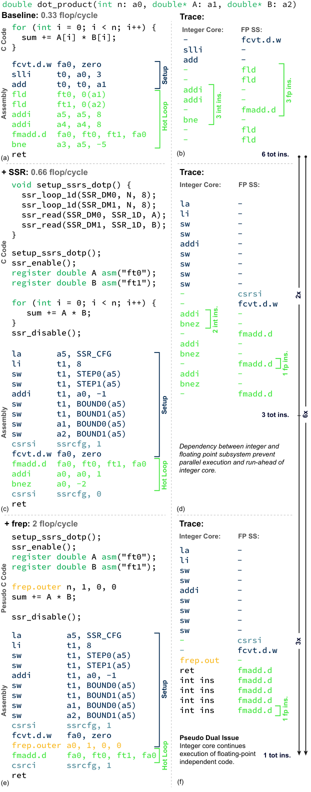
Changing environments require a programmable system. To avoid overspecialization, we propose a system composed of many programmable and highly energy-efficient processing elements by leveraging widely applicable ISA extensions. At the foundation, the proposed system is a general-purpose RISC-V-based multi-core system. The system has no private data caches but offers a fast, energy-efficient, and high-throughput software managed TCDM as an alternative. It can be efficiently programmed using a RISC-V toolchain, see Figure 6(a). The hardware provides atomic memory operations as defined by RISC-V for efficient multi-core programs. The program operates on physical addresses with a minimal runtime.
The SSR and FREP extension can be used with the provided header-only C library using an intrinsic-like style, similar to the RISC-V vector intrinsics currently under development [27]. A set of, hand-tuned library routines can be used to exploit the proposed SSR and FREP hardware extensions for optimal benefit of the proposed ISA extensions, similar to the cuBLAS or cuDNN libraries provided for Nvidia’s GPUs. Furthermore, a first Low Level Virtual Machine (LLVM) prototype shows that automatic code generation for SSR setup is feasible [17].
III-A Stream Semantic Registers
We provide a small, header-only, software library to program the SSR efficiently. In particular, the programmer can decide the dimension of the stream and select the appropriate library function. For each dimension, the programmer needs to provide a stride, a bound, and a base address to configure the streamer. Finally a write to the SSR CSR activates the stream semantic on register ft0 and ft1. After the streaming operation finishes, the same CSR is cleared to deactivate the extension. The whole programming sequence for an example kernel is depicted in Figure 6(c). On the example of the dot product kernel, we can see the speed-up of using the SSR extension over the baseline implementation. The vanilla RISC-V implementation executes a total of six instructions in its innermost loop, of which three are integer, and three are floating-point instructions, see Figure 6(b). The SSR-enhanced version, on the other hand, elides all loads and only needs to track one loop counter to determine the loop termination condition. This saves three instructions and provides a 2x speed-up. The loop setup overhead is slightly higher, and a detailed analysis can be found in the original SSR paper [17]. For this system, we have enhanced the SSR system to provide the programmer with shadow registers for the loop configuration. Therefore, the integer core can already set up the next loop iteration and store the configuration in the shadow registers while the current iteration is still in progress. When the current iteration finishes, the SSR configuration logic automatically starts the iteration for the new configuration.
III-B FPU Sequencer
The frep instruction configures the FPU sequencer to automatically repeat and autonomously issue the next floating-point instructions to the FPU. This completely elides all loop instructions in the innermost loop iteration as the branch decision and loop counting is pushed to the sequencer hardware. For the dot product example, this only leaves one instruction in the innermost loop and provides a speed-up of compared to the baseline, and a improvement over the plain SSR version of the kernel see Figure 6(f). As the FPU sequencer frees the integer core of issuing instructions to the FP-SS, it can continue executing integer instructions. This makes the core pseudo dual-issue, see Figure 6(f). The pseudo-dual issue is a property of the decoupled design of FP-SS and integer core: Both subsystems will execute as many instructions in parallel until they detect a blocking event such as a data movement from or to the FP-SS and a dependent instruction.
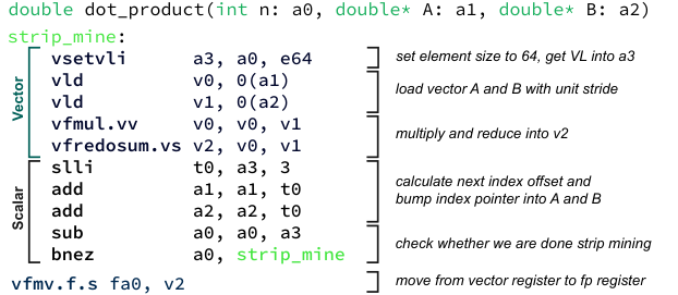
For the same dot product kernel, we have also listed the corresponding RISC-V vector assembly as a comparison point, see Figure 7. Depending on the hardware’s maximum VL and the problem size, software needs to perform a strip mine loop over the input data. For each iteration, the setvl instruction saves the number of elements of subsequent vector instructions into its destination register. The integer core performs bookkeeping and pointer arithmetic for each iteration. Of the ten instructions of the strip mine loop, only five execute on the vector unit, of which only two perform arithmetic operations.
III-B1 Operand Staggering
The complex floating-point operations performed by the FPU require pipelining to achieve reasonable clock frequencies. Pipelining, on the other hand, increases the latency of floating-point instructions, which makes it impossible for one floating-point instruction to directly re-use the result of the previous instruction without stalling the pipeline. Depending on the speed target, we expect between two and six pipeline stages for floating-point multiply-add. Therefore the next operation would need to wait for the same number of cycles until the operand becomes available. Some of these stalls can be hidden by executing independent floating-point operations in the meantime. This technique requires partial unrolling of the kernel. To combine this efficiently with the FREP extension, we provide an option for the sequencer to stagger its operands. The staggering logic automatically increases the operand names of the issued instruction by one. The frep command takes an additional stagger mask and stagger count. The mask defines which register should be staggered. The mask contains one bit for all three source operands and the destination operand, four bits in total. If the corresponding bit is set, the FPU sequencer increases the register name by one until the stagger count has been reached. Once the count is reached, the register name wraps again. The anatomy of the frep instruction including a sample trace with staggering enabled can be seen in Figure 5 (a).
IV Results
We have synthesized, placed and routed an eight core configuration with two hives (each with four cores), of TCDM, and of instruction cache using the Synopsys Design Compiler 2017.09 and Cadence Innovus 17.11 in a modern Globalfoundries 22 nm FDX technology. The floorplan of this cluster is depicted in Figure 8. For the synthesis we have constrained the design to close timing at in worst case conditions (SSG22 2 p-channel metal–oxide–semiconductor field-effect transistor (MOSFET) globally slow, n-channel MOSFET globally slow, , ). The subsequent place and route step was constrained to . Sign-off static timing analysis (STA) using Synopsys Primetime 2019.12 showed that the design runs at in worst case conditions and in typical conditions (TT33 3 p-channel MOSFET typical, n-channel MOSFET typical, , ).

IV-A Microkernels
To evaluate the performance, power, and energy-efficiency of the architecture, we have implemented a set of different data-oblivious parallel benchmarks, where the control flow only depends on a constant number of program parameters. We selected four complementary kernels:
- •
Dot product: A simple dot product implementation that calculates the scalar product of two arrays of length . Included because it is a fundamental vector-vector operation (basic linear algebra subprograms (blas) 2).
- •
ReLU: This kernel applies a rectified linear unit (ReLU) to the elements of an array of length . The kernel is often used as an activation function for neural networks ( blas ).
- •
Matrix multiplication using the dot product method: A chunked implementation of matrix multiplication of size . A highly relevant kernel for the machine learning domain (blas 3). The output matrix is chunked across the cores.
- •
FFT: Implementation of a parallel FFT algorithm of size . Included to show the versatility of the tightly coupled core and the proposed extensions. The FFT is based on Cooley–Tukey’s algorithm.
- •
AXPY () on vectors of length : Included as a memory-bound kernel. As the benchmarked system only provides two SSRs, the core needs to perform the store operation, which prevents any speed-ups from FREP. Furthermore, the kernel is memory-bound as it requires three memory accesses per two floating-point operations but each core can only sustain two memory operations through its two ports in the TCDM interconnect (blas 1).
- •
kNN: This algorithm performs a point-wise Euclidean distance calculation between all points () in the system and a sample. In a second sorting step, the closest points are returned as classification results. The SSR +FREP can significantly speed-up the Euclidean distance calculation. However, the dominant factor of the over-all runtime is the sorting step, which can not easily be accelerated using SSR and FREP. To provide maximum insight into the achievable improvement, we focused our measurements on the distance calculation. Parallelization is achieved by distributing the sampling step amongst all cores.
- •
Monte Carlo method approximating in steps. The integer core generates random numbers while the floating-point subsystem evaluates the function to be integrated. SSR and FREP make for an exciting application since the pseudo-dual issue allows the two tasks to entirely overlap and execute in parallel on the integer core and floating-point subsystem, respectively. Interestingly, we see a slight drop in speed-up in the pure SSR case because the problem needs to be re-formulated for SSR usage, which in turn exhibits an adversarial instruction pattern in the FP-SS (many dependent floating-point instructions).
- •
2D Convolution on a image with a kernel (kernel size is from the first layer of Google LeNet, the input image size has been truncated to reduce the problem runtime): A highly relevant workload for the machine-learning and data-science domain. The high data-reuse and affine access pattern make it an ideal candidate for enhancement with SSRs and FREP.
For each kernel we provide a baseline C implementation44 4 riscv32-unknown-elf-gcc (GCC) 7.2.0 -03 (without auto-vectorization or special intrinsics), an implementation which makes use of SSRs and one which combines SSRs and FREP. We have made sure (partially by using inline-assembly) that the generated baseline code is optimal and executes well on the Snitch core. Speed-ups are measured in a cycle-accurate register transfer level (RTL) simulation, similarly power estimations are measured in a post-layout simulation. All the kernels input and output data set sizes are chosen so that they fit into the TCDM to avoid measuring effects of the cluster-external memory hierarchy.
IV-B Single-Core
IV-B1 Performance
| Utilization | |||||||||
|---|---|---|---|---|---|---|---|---|---|
| Single-Core | Multi-Core (8 Cores) | ||||||||
| Kernel | FPU | FPSS | Snitch | IPC | FPU | FPSS | Snitch | IPC | |
| Dot Pr. | 0.17 | 0.50 | 0.50 | 1.00 | 0.20 | 0.58 | 0.22 | 0.80 | |
| + SSR | 0.61 | 0.63 | 0.35 | 0.98 | 0.35 | 0.38 | 0.32 | 0.69 | |
| + SSR + FREP | 0.87 | 0.89 | 0.06 | 0.96 | 0.35 | 0.41 | 0.18 | 0.59 | |
| Dot Pr. | 0.25 | 0.75 | 0.25 | 1.00 | 0.24 | 0.70 | 0.24 | 0.94 | |
| + SSR | 0.66 | 0.66 | 0.34 | 1.00 | 0.57 | 0.58 | 0.32 | 0.90 | |
| + SSR + FREP | 0.98 | 0.99 | 0.01 | 0.99 | 0.72 | 0.74 | 0.05 | 0.79 | |
| ReLU | 0.14 | 0.42 | 0.57 | 1.00 | 0.13 | 0.37 | 0.53 | 0.90 | |
| + SSR | 0.32 | 0.32 | 0.67 | 0.99 | 0.23 | 0.23 | 0.56 | 0.79 | |
| + SSR + FREP | 0.88 | 0.89 | 0.07 | 0.96 | 0.36 | 0.36 | 0.23 | 0.62 | |
| DGEMM | 0.19 | 0.58 | 0.17 | 0.75 | 0.17 | 0.51 | 0.15 | 0.66 | |
| + SSR | 0.23 | 0.26 | 0.53 | 0.80 | 0.20 | 0.23 | 0.49 | 0.72 | |
| + SSR + FREP | 0.86 | 0.97 | 0.07 | *1.04 | 0.63 | 0.71 | 0.13 | 0.84 | |
| DGEMM | 0.24 | 0.26 | 0.52 | 0.77 | 0.24 | 0.26 | 0.51 | 0.77 | |
| + SSR | 0.24 | 0.26 | 0.52 | 0.77 | 0.24 | 0.26 | 0.51 | 0.77 | |
| + SSR + FREP | 0.93 | 0.99 | 0.03 | *1.02 | 0.85 | 0.90 | 0.04 | 0.94 | |
| FFT | 0.36 | 0.49 | 0.23 | 0.72 | 0.26 | 0.35 | 0.23 | 0.58 | |
| + SSR | 0.54 | 0.58 | 0.32 | 0.90 | 0.21 | 0.23 | 0.41 | 0.65 | |
| + SSR + FREP | 0.57 | 0.62 | 0.19 | 0.81 | 0.24 | 0.27 | 0.42 | 0.69 | |
| AXPY | 0.19 | 0.77 | 0.20 | 0.97 | 0.14 | 0.63 | 0.19 | 0.82 | |
| + SSR | 0.34 | 0.67 | 0.27 | 0.95 | 0.23 | 0.47 | 0.30 | 0.77 | |
| 2D Conv. | 0.14 | 0.43 | 0.57 | 1.00 | 0.14 | 0.42 | 0.58 | 1.00 | |
| + SSR | 0.60 | 0.60 | 0.39 | 0.99 | 0.60 | 0.61 | 0.39 | 0.99 | |
| + SSR + FREP | 0.97 | 0.99 | 0.04 | *1.03 | 0.91 | 0.93 | 0.04 | 0.97 | |
| kNN | 0.15 | 0.31 | 0.40 | 0.70 | 0.14 | 0.31 | 0.40 | 0.70 | |
| + SSR | 0.30 | 0.30 | 0.64 | 0.95 | 0.30 | 0.31 | 0.66 | 0.97 | |
| + SSR + FREP | 0.35 | 0.36 | 0.76 | *1.13 | 0.35 | 0.37 | 0.79 | *1.16 | |
| Monte Carlo | 0.14 | 0.18 | 0.59 | 0.77 | 0.13 | 0.16 | 0.54 | 0.70 | |
| + SSR | 0.15 | 0.21 | 0.61 | 0.82 | 0.14 | 0.20 | 0.57 | 0.77 | |
| + SSR + FREP | 0.22 | 0.22 | 0.90 | *1.12 | 0.20 | 0.20 | 0.82 | *1.02 | |
- *
Pseudo-dual issue behavior with a cumulative IPC higher than one
-
Reduction of FPU utilization because of SSR setup and frequent re-synchronization between FFT stages. We still show a speed-up of (see Figure 13)
-
AXPY can not be enhanced using FREP because the current architecture provides only two streamers. For the AXPY kernel three streamers would be needed.
The single-pipeline stage of the core lets it achieve a very high IPC of close to one for most of the kernels. The only effective source of stalls comes from the memory interface if there is a load-use dependency present or when the load result contends for the single write port of the core’s RF. The proposed ISA extensions, SSR, and FREP reduce the number of explicit load and store instructions as well as the branching overhead. For above-mentioned microkernels we can report single-core speed-ups of over 6x in Figure 9 on certain benchmarks. The single-core case presents an idealized execution environment as there is no contention on the shared TCDM. We observe interesting effects: The matrix multiplication, 2D convolution, kNN distance calculation, and the Monte Carlo benchmark achieve an IPC of more than one by overlapping the computation of one block with the SSR setup and integer instructions of the next block.
In Table I we are tracking four metrics:
- 1.
FPU utilization: The total number of arithmetic floating-point instructions executed. We consider (fused) arithmetic operations, casts, and comparison instructions as floating-point operations.
- 2.
FP-SS utilization: Includes all instructions that are off-loaded to the FP-SS. This counts all floating-point instructions as well as floating-point loads and stores.
- 3.
Snitch utilization: Contains all instructions that are not offloaded to the FP-SS.
- 4.
Total IPC: Snitch utilization and FP-SS utilization result in the total IPC. For the baseline case, this metric is interesting as due to the single pipeline stage and the tightly coupled memory subsystem we achieve an IPC of one for almost every kernel in the single-core case. For the multi-core system, contentions on the memory interface slightly limit the attainable IPC. This ensures a fair baseline for further evaluating our ISA extensions. The reported IPC for the FREP enhanced kernels includes the FREP generated instructions.
The single-issue nature of the baseline core limits the maximum achievable FPU utilization as we need to explicitly move data from memory into the core’s register file. This ranges from to depending on the benchmark. We can see a very high core utilization as the integer core is supplying the FPU with instructions.
The introduction of SSR relaxes these constraints as we are translating all loads and stores into implicitly encoded register reads. We can see a positive effect on execution time as we are not using an issue slot (cycle) of the integer core to issue load(s)/store(s). We can still see that the integer core is busy issuing arithmetic floating-point instructions to the FPU by observing a high Snitch utilization.
Finally, with the introduction of FREP, we significantly reduce the pressure on the integer core. The integer core only issues the floating-point operations once into the frep buffer from which it is being sequenced multiple times to the FP-SS. We can observe a very low integer core utilization of somewhere between . As we free the integer core from issuing floating-point instructions on every cycle, we can easily keep the FPU busy. This results in a very high FPU utilization of . A high FPU utilization, in turn, means high energy efficiency. For the single-core case we can see an improvement in speed-up (see Figure 9) and FPU utilization for all microkernels. The FFT benchmark shows a reduction in IPC as more frequent SSR set-up and load-use dependencies insert stall cycles which result in pipeline bubbles.
IV-B2 Area

The integer core ISA is configurable to either be RV32I or RV32E. Both support the same instructions but differ in the size of the RF. While RV32I comes with 32 general purpose integer register, RV32E only provides 16. As the CPU design is heavily dominated by the RF (see Figure 10) this design choice has a significant influence on the core’s area. Furthermore, as mentioned in Section II-A1 we provide a latch-based and a FF-based RF implementation. The first being smaller in area while the latter can be used if latches are not available in the standard-cell library. Moreover, PMCs can be enabled separately which adds approximately in area. Altogether this makes the integer core configurable from (RV32E, latch-based RF without PMC) up to (RV32I, flip-flop-based RF with PMC), see Figure 11. The SSR hardware consumes to implement address generation and control logic as well as load data buffering. This puts it at of the FP-SS and of the CC. The FREP extension, configured with entries, takes up which is of the FP-SS’s area and of the overall system on chip (SoC) (a total of for the CC).
IV-C Multi-Core
IV-C1 Performance
| # Cores | # Cores | ||||||||
|---|---|---|---|---|---|---|---|---|---|
| 1 | 0.89 | 1.00 | 1.00 | 8 | 0.87 | 2.00 | 7.80 | ||
| 2 | 0.90 | 1.98 | 1.98 | 16 | 0.81 | 1.87 | 14.62 | ||
| 4 | 0.87 | 1.97 | 3.91 | 32 | 0.82 | 1.89 | 27.61 |
| 4 FPUs | 8 FPUs | 16 FPUs | |||||||
|---|---|---|---|---|---|---|---|---|---|
| Snitch | Ara | Hwacha* | Snitch | Ara | Hwacha | Snitch | Ara | Hwacha | |
| 16 | 68.2 | 49.5 | — | 63.2 | 25.4 | — | 58.3 | 12.8 | — |
| 32 | 87.1 | 82.6 | 49.9 | 84.8 | 53.4 | 35.6 | 81.4 | 27.6 | 22.4 |
| 64 | 93.4 | 89.6 | — | 91.7 | 77.5 | — | 89.0 | 45.6 | — |
| 128 | 96.0 | 94.3 | — | 94.7 | 93.1 | — | 94.1 | 78.8 | — |
- *
Performance results extracted from [28]
For the multi-core performance evaluations we have instantiated an eight core cluster with of instruction cache and of TCDM memory (see Figure 8).
Parallelization
We have parallelized our kernels to distribute work evenly on all cores. Synchronization between cores is achieved using RISC-V’s atomic extension and support for atomics on the TCDM and on AXI using AXI5’s atomic extension and an atomic adapter [29]. Depending on the workload, parallelization achieves a speed-up from up to for the measured octa-core cluster compared to the single-core version (see Figure 12). Ideal speed-ups of eight are achieved for the pure SSR 2D convolution and the kNN baseline. High multi-core speed-ups can be achieved for matrix multiplication, 2D convolution, kNN, and Monte Carlo methods. The FFT, dot product and AXPY kernels do not scale that well, mostly due to small problem size which amplifies the reduction and synchronization impact on the overall runtime.
Multi-core speed-up with SSR and FREP
As can be seen in Figure 13 we achieve speed-ups from to depending on the benchmark. As in the single-core case we can use the proposed SSR and FREP extensions to elide explicit load/stores and control flow instructions. In contrast to the single-core case (Figure 9) we can observe a slight reduction in speed-up as operand values are potentially (temporarily) unavailable due to contentions on the shared TCDM (SRAM bank conflicts), as well as effects of Amdahl’s law. Furthermore, we achieve over FPU utilization for matrices of size . As can be seen in Table III we significantly, by a factor of , outperform existing vector processors on small matrix multiplication problems. On larger problems we can show equal or better performance.
The FFT benchmark demonstrates that the proposed ISA extensions are also applicable on less linear problems such as FFT. While we see a decreased FPU utilization in the multi-core system (Table II) we can observe a total speed-up of . The decreased FPU utilization is attributable to the less linear access pattern and the higher core synchronization frequency for each FFT stage, which in turn leads to higher contentions as cores are forced to start fetching at the same time from the same memory bank upon each (re-)synchronization.
The Monte Carlo problem is interesting as the pure SSR version is slower than the baseline. This is attributed to the fact that the problem needs to re-formulated to operate on blocks of random input data to be beneficial to the streamer infrastructure. The block-wise operation in contrast exhibits floating-point data dependencies which could have been filled with integer instructions in the baseline case. Finally, the introduction of FREP can then fully exploit the fact that integer and floating-point pipeline can be executed in parallel exhibiting pseudo-dual-issue behavior. The algorithm is still dominated by the integer core generating good random numbers which effectively limits the overall speed-up (we use the xoshiro128+ linear pseudorandom number generator introduced by Blackman and Vigna [30]). The RISC-V bit-manipulation extension or a special function unit (SFU) dedicated to generating (good) random numbers could significantly enhance this kernel’s speed-up.
IV-C2 Area
While the impact of the FREP extension is confined to CC the SSR extension also has a cluster-level impact. With SSR enabled, each core has two ports into the TCDM, increasing the area of the fully connected interconnect. In the selected implementation of an eight-core cluster, we have 16 request ports and 32 memory banks (providing a banking-factor of two). With the TCDM interconnect occupies of the overall area. The complexity of the crossbar scales with the product of its master and slave ports. We have estimated the complexity of a requests and banks crossbar to be around and the area of a request ports and banks to be around .
IV-C3 Energy Efficiency and Power

We have selected a matrix multiplication benchmark running on a post-layout netlist to give an indicative power break-down of the system’s component (Figure 14). For the given benchmark the cluster consumes a total of of which are consumed in the CC, in the interconnect and in the SRAM banks of the TCDM. of the energy is spent in the actual FPU on the computation. While the integer control core only uses of the overall power. The additional hardware for SSR and FREP only make up for a fraction of the overall power consumption, less than and respectively. What is particularly interesting ist that the instruction cache only consumes or of the total cluster power. This is due to the FREP extension servicing the FPU from its local sequence buffer, and the Snitch integer core exhibiting a very low activity that can mostly be served from its L0 instruction cache, that has been implemented as a FF-based memory and can be read and written using less energy compared to SRAMs. The total power of all micro-benchmarks is given in Figure 15. As we only see a marginal increase in power for the given benchmarks but a significant improvement in execution speed and a high FPU utilization we can observe a similiar increase in energy efficiency. Figure 16 shows a increase in energy efficiency compared to the baseline. The systems achieves an absolute peak energy efficiency of close to and for double precision matrix multiplication and up to for the 2D convolution benchmark.
To put the absolute energy efficiency into perspective, we estimated the achievable peak energy efficiency in . Every architecture, even highly specialized accelerators, must at least perform two loads and a FMA instruction for each element. We can, therefore, estimate the energy-efficiency upper bound of . Snitch achieves of this theoretical peak efficiency.
V Related Work
| Snitch | Ara | Volta SM | Carmel* | |||
| Unit | Us | [14] | [31] | [31] | ||
| Problem Size | 32 | 32 | 256 | 256 | ||
| Base ISA | RV | RV | Volta | Arm | ||
| Technode | [] | 22 | 22 | 12 | 12 | |
| Clock (typical) | [] | 1.06 | 1.17 | 1.38 | 2.27 | |
| Clock (worst) | [] | 0.75 | 0.87 | — | — | |
| Peak SP | [] | 16.96 | 18.72 | 176 | 36.25 | |
| Peak DP | [] | 16.96 | 18.72 | — | 18.13 | |
| Sustained SP | [] | 14.38 | 10.00 | 153 | §22.10 | |
| Sustained DP | [] | 14.38 | 10.00 | — | 9.27 | |
| Utilization SP | [] | 84.80 | — | 86.66 | 60.97 | |
| Utilization DP | [] | 84.80 | 53.40 | — | 51.15 | |
| Impl. Area# | [] | 0.89 | 1.07 | 11.03 | **7.37 | |
| Area Eff. SP | [] | 25.83 | — | 13.84 | 3.00 | |
| Area Eff. DP | [] | 25.83 | 17.53 | 13.84 | 1.26 | |
| Tot. Power SP | [] | 0.13 | — | 2.91 | 2.16 | |
| Tot. Power DP | [] | 0.17 | 0.46 | — | 1.85 | |
| Leakage | [] | 12 | 21.1 | — | — | |
| Energy Eff. SP | [] | 103.84 | — | 52.39 | 10.24 | |
| Energy Eff. DP | [] | 79.42 | 39.9 | — | 5.01 |
- *
Single-core, estimated from the eight core core complex including L3 cache
-
The Volta SM in Tegra Xavier does not contain any double precision FPUs
-
Measured using the SGEMM implementation of CUBLAS [32]
- §
Measured using an SGEMM implementation of the ARM ComputeLibary using NEON ISA extension [33]
-
Measured using the OpenBLAS implementation [34]
- #
Post-layout area measured from die photograph
- **
Including proportionate L2 and L3 caches
The problem of keeping the FPU utilization high has been the subject of a lot of architecture research. The most prominent and widely used techniques encompass super-scalar (out-of-order), general-purpose, CPUs, (Cray-style) vector architectures and general-purpose compute using GPUs. While these architectures promise to deliver high performance, they do not target energy efficiency as their primary design goal.
V-A Vector Architectures
Cray-style vector architectures are enjoying renewed popularity with Arm providing their SVE [13] and RISC-V actively developing a vector extension [26]. An early, but complete version of the RISC-V vector extension in called Ara, has been implemented by Cavalcante et al. [14]. The same technology node and configuration size allow for a direct comparison to our architecture. As a comparison point, we chose an eight-lane configuration that delivers a peak of equal to the octa-core cluster we have presented in the evaluation section. The vector architecture accelerates programs that work on vectored data by providing a single-instruction which operates on (parts of) the vector. The instruction front-end of the attached core is feeding the vector unit special vector instructions that can then independently operate on chunks of data from the vector register file. The vector register file is similar in size and access latency to the TCDM in a Snitch cluster. However, in stark contrast to the vector register file, our system allows us to access individual elements of the TCDM as it is byte-wise addressable. The vector architecture compensates this fact by providing dedicated shuffle instructions, which, in contrast, consume precious instruction bandwidth and issue-slots.
As a consequence, the scalar core needs to issue many instructions to the vector architecture that potentially bottleneck the instruction front-end and hence performs poorly on smaller and finer granular problems (see Table III). On smaller matrix multiplication problems, our architecture significantly outperforms, by a factor of 4.5, the Ara vector architecture as our TCDM interconnect and byte-wise access to the TCDM provides implicit shuffle semantic. On increasing problem sizes, the vector architecture catches up in performance, but we can retain superiority even for larger problem sizes (see Table III).
The rigid, linear access pattern, superimposed by the nature of vectors, imposes yet another problem: To compensate for the lack of access semantic into the register file additional ISA extensions such as 2D and tensor extensions are needed to encode the more complicated access patterns. As the shape of the computation is encoded in the instruction, this significantly bloats the encoding space, which in turn makes the instruction-frontend and decoding logic more complex and hence more energy-inefficient. In contrast the SSR and FREP extension provide up to 4 access dimensions in their current implementation. With the implicit load/store encoding into register reads/writes, no new instructions are needed, and the instruction-frontend and decoding logic is identical to the scalar core.
Table IV compares several figures of merit between Ara (Ariane’s vector extension) and the same size Snitch system. Both systems offer the same number of floating-point operations per cycle at comparable clock-frequency. On the chosen problem size of a matrix multiplication, our system offers more than sustained floating-point operations at twice the energy efficiency of almost compared to of Ara. A similar comparison can be done for the axpy and 2D convolution benchmark, where we achieve and the energy efficiency improvement over Ara. Most of the energy efficiency gains come from the higher area efficiency and the much higher compute/control ratio. A comparable architecture to Ara is Hwacha [28], which suffers from similar limitations.
V-B GPUs
GPUs have completely penetrated the market of general-purpose computing with their superior capabilities to accelerate dense linear algebra kernels most prominently found in machine-learning applications. The key idea of General Purpose Computation on Graphics Processing Unit (GPGPU) is to oversubscribe the compute units using multiple, parallel threads that can be dynamically scheduled by hardware to hide access latencies to memory. We have estimated energy efficiency of an NVIDIA GPU using a Tegra Xavier SoC [31] development kit. The board allows for direct power measurements on the supply rails of both the GPU and CPU. The Tegra SoC contains a Volta-based [35] GPU consisting of eight SMs which each in turn consists of 32 double- and 64 single-precision FPUs. Each SM contains four execution units, each managing eight double-precision and 16 single-precision FPUs, which share a common register file and an instruction cache. Hence such a quadrant is directly comparable to one Snitch cluster as presented here. Clock speeds of of Snitch and for the Volta SM are comparable keeping in mind that the SM has been manufactured in a more advanced technology, see Table IV. On a high-level comparison, the Snitch system surpasses the SM in terms of energy efficiency, by over on single-precision workloads. This comparison does not take technology scaling into consideration, which would further improve energy-efficiency in favor of Snitch.
V-C Super-scalar CPUs
The Tegra Xavier SoC also offers an eight-core cluster of NVIDIA’s ARMv8 implementation called Carmel. The Carmel CPU is a 10-issue, super-scalar CPU including support for Arm’s SIMD extension NEON. Each core contains two 128-bit SIMD-FPUs that are fracturable in either two 64-bit, four 32-bit or eight 16-bit units, offering a total of 8 double-precision , hence comparable to the presented octa-core Snitch cluster. The processor runs at a substantially higher clock frequency of at the expense of a much deeper pipeline, which in turn requires the processor to hide pipeline stalls by exploiting instruction level parallelism (ILP) in the form of super-scalar execution and a steep memory hierarchy to mitigate the effects of high memory latency. The increased hardware cost reduces the attainable area efficiency to only . The losses in area efficiency have a direct influence on the energy efficiency of the system. Not accounting for technology scaling, we can show more than improvement in energy efficiency for FP32 and for FP64.
Recent developments in high-performance chips, such as Fujitsu’s A64FX [36], clearly demonstrate that energy-efficiency is becoming the number one design concern. The new Green500 [37] winner achieves system-level energy-efficiency (including cooling, board and power supplies). Unfortunately, as we do not have access to such a system for detailed measurements, we can not perform accurate direct comparisons.
VI Conclusion
We present a general-purpose computing system tuned for the highest possible energy efficiency on double-precision floating-point arithmetic. The system offers an implementation of the RISC-V atomic extension (A) for efficient multi-core programming and can be targeted with a standard RISC-V toolchain. We outperform existing state-of-the-art systems (Table IV on energy efficiency by a factor of by leveraging several ideas.
Tightly Coupled Data Memory (TCDM)
Explicit scratchpad memories (TCDM) instead of hardware managed caches enable deterministic data placement and avoid suboptimal cache replacement strategies. The TCDM memory is shared amongst a cluster of cores, making data sharing significantly more energy efficient as no cache coherence protocol is necessary.
Small and efficient integer core
We aim to maximize the control to compute ratio by providing a small and agile integer core that can do single-cycle control flow decisions and integer arithmetic and combine it with a large FPU. The FP-SS decouples the integer/control flow from the floating-point operations and the FP-SS can operate on its own register file and provides its own floating-point (FP) LSU.
ISA extensions
We provide two minimal impact ISA extensions, SSRs and FREP. The first makes it possible to set up a four-dimensional stream to memory from which the core can simply read/write using two designated register names. The FREP extension complements the SSR extension by further decoupling the issuing of floating-point instructions to the FP-SS. The integer core pushes RISC-V instructions into the previously configured loop-buffer and subsequently issue those instructions to the FPU. This has two beneficial side-effects: While the FPU loop-buffer feeds the FPU with instructions, the integer core is free to do auxiliary tasks, such as orchestrating data movement. The second positive effect is that it relieves the pressure on the instruction cache, therefore saving energy.
The system achieves a speed-up of up to on data-oblivious kernels while still being fully programmable and not overspecializing on one problem domain. The flexibility offered by the small, integer control unit makes it a versatile architecture and possible to adapt to changing algorithmic requirements. Furthermore, we have shown that eight cores per cluster provide a good trade-off between speed-up and complexity of the interconnect (see Table II and Section IV-C2). A future extension of the proposed SSR hardware could target improved efficiency for sparse linear algebra problems. Furthermore, extended benchmarking and improvements in the compiler infrastructure are exciting future research directions.
Acknowledgments
This work has received funding from the European Union’s Horizon 2020 research and innovation programme under grant agreement number 732631, project “OPRECOMP”.
References
- [1] Y. Yao and Z. Lu, “Pursuing Extreme Power Efficiency with PPCC Guided NoC DVFS,” IEEE Transactions on Computers, 2019.
- [2] A. Fuchs and D. Wentzlaff, “The accelerator wall: Limits of chip specialization,” in 2019 IEEE International Symposium on High Performance Computer Architecture (HPCA). IEEE, 2019, pp. 1–14.
- [3] T. Nowatzki, V. Gangadhan, K. Sankaralingam, and G. Wright, “Pushing the limits of accelerator efficiency while retaining programmability,” in 2016 IEEE International Symposium on High Performance Computer Architecture (HPCA). IEEE, 2016, pp. 27–39.
- [4] J. L. Hennessy and D. A. Patterson, Computer architecture: a quantitative approach. Elsevier, 2011.
- [5] C. Celio, P.-F. Chiu, B. Nikolic, D. Patterson, and K. Asanovic, “BOOM v2,” 2017.
- [6] J. Zhao, B. Korpan, A. Gonzalez, and K. Asanovic, “Sonicboom: The 3rd generation berkeley out-of-order machine.”
- [7] T. Singh, S. Rangarajan, D. John, R. Schreiber, S. Oliver, R. Seahra, and A. Schaefer, “2.1 zen 2: The amd 7nm energy-efficient high-performance x86-64 microprocessor core,” in 2020 IEEE International Solid- State Circuits Conference - (ISSCC), 2020, pp. 42–44.
- [8] F. Zaruba and L. Benini, “The Cost of Application-Class Processing: Energy and Performance Analysis of a Linux-Ready 1.7-GHz 64-Bit RISC-V Core in 22-nm FDSOI Technology,” IEEE Transactions on Very Large Scale Integration (VLSI) Systems, pp. 1–12, 2019.
- [9] M. Gautschi, P. D. Schiavone, A. Traber, I. Loi, A. Pullini, D. Rossi, E. Flamand, F. K. Gürkaynak, and L. Benini, “Near-threshold RISC-V core with DSP extensions for scalable IoT endpoint devices,” IEEE Transactions on Very Large Scale Integration (VLSI) Systems, vol. 25, no. 10, pp. 2700–2713, 2017.
- [10] M. Cornea, “Intel AVX-512 instructions and their use in the implementation of math functions,” Intel Corporation, 2015.
- [11] V. G. Reddy, “Neon technology introduction,” ARM Corporation, vol. 4, no. 1, 2008.
- [12] R. M. Russell, “The CRAY-1 computer system,” Communications of the ACM, vol. 21, no. 1, pp. 63–72, 1978.
- [13] N. Stephens, S. Biles, M. Boettcher, J. Eapen, M. Eyole, G. Gabrielli, M. Horsnell, G. Magklis, A. Martinez, N. Premillieu et al., “The ARM scalable vector extension,” IEEE Micro, vol. 37, no. 2, pp. 26–39, 2017.
- [14] M. Cavalcante, F. Schuiki, F. Zaruba, M. Schaffner, and L. Benini, “Ara: A 1 GHz+ Scalable and Energy-Efficient RISC-V Vector Processor with Multi-Precision Floating Point Support in 22 nm FD-SOI,” arXiv preprint arXiv:1906.00478, 2019.
- [15] NVIDIA, “Tesla V100 GPU Architecture Whitepaper,” August 2017, accessed: September 2019. [Online]. Available: https://images.nvidia.com/content/volta-architecture/pdf/volta-architecture-whitepaper.pdf
- [16] Z. Jia, M. Maggioni, B. Staiger, and D. P. Scarpazza, “Dissecting the nvidia volta gpu architecture via microbenchmarking,” arXiv preprint arXiv:1804.06826, 2018.
- [17] F. Schuiki, F. Zaruba, T. Hoefler, and L. Benini, “Stream Semantic Registers: A Lightweight RISC-V ISA Extension Achieving Full Compute Utilization in Single-Issue Cores,” 2019.
- [18] O. Goldreich and R. Ostrovsky, “Software protection and simulation on oblivious RAMs,” Journal of the ACM (JACM), vol. 43, no. 3, pp. 431–473, 1996.
- [19] I. Corporation, “Intel 64 and IA-32 Architectures Software Developer’s Manual,” [Online]. Available: https://www.intel.com/content/dam/www/public/us/en/documents/manuals/64-ia-32-architectures-software-developer-instruction-set-reference-manual-325383.pdf.
- [20] D. TMS320C28x, “Cpu and instruction set reference-guide (rev. c),” Texas lnstruments, vol. 5, 2004.
- [21] M. B. Taylor, “Basejump STL: systemverilog needs a standard template library for hardware design,” in Proceedings of the 55th Annual Design Automation Conference. ACM, 2018, p. 73.
- [22] A. Gonzalez, F. Latorre, and G. Magklis, “Processor microarchitecture: An implementation perspective,” Synthesis Lectures on Computer Architecture, vol. 5, no. 1, pp. 1–116, 2010.
- [23] C. Wolf, “RISC-V Formal Verification Framework,” 2019. [Online]. Available: https://github.com/SymbioticEDA/riscv-formal
- [24] S. Mach, F. Schuiki, F. Zaruba, and L. Benini, “A 0.80pj/flop, 1.24tflop/sw 8-to-64 bit transprecision floating-point unit for a 64 bit risc-v processor in 22nm fd-soi,” in 2019 IFIP/IEEE 27th International Conference on Very Large Scale Integration (VLSI-SoC), Oct 2019, pp. 95–98.
- [25] F. Schuiki, M. Schaffner, F. K. Gürkaynak, and L. Benini, “A scalable near-memory architecture for training deep neural networks on large in-memory datasets,” IEEE Transactions on Computers, vol. 68, no. 4, pp. 484–497, 2018.
- [26] RISC-V Vector Task Group, “Risc-v vector extension,” https://github.com/riscv/riscv-v-spec, 2020.
- [27] BSC, “RISC-V Vector Intrinsics,” 2020. [Online]. Available: https://repo.hca.bsc.es/gitlab/rferrer/epi-builtins-ref/blob/master/epi-builtins-ref.md
- [28] D. Dabbelt, C. Schmidt, E. Love, H. Mao, S. Karandikar, and K. Asanovic, “Vector processors for energy-efficient embedded systems,” in Proceedings of the Third ACM International Workshop on Many-core Embedded Systems. ACM, 2016, pp. 10–16.
- [29] A. Kurth, S. Riedel, F. Zaruba, T. Hoefler, and L. Benini, “Atuns: Modular and scalable support for atomic operations in a shared memory multiprocessor.”
- [30] D. Blackman and S. Vigna, “Scrambled linear pseudorandom number generators,” arXiv preprint arXiv:1805.01407, 2018.
- [31] M. Ditty, A. Karandikar, and D. Reed, “Nvidia’s xavier SoC,” in Hot Chips: A Symposium on High Performance Chips, 2018.
- [32] C. Nvidia, “CUBLAS library programming guide,” NVIDIA Corporation. edit, vol. 1, 2007.
- [33] P. Charles, “Computelibrary,” https://github.com/ARM-software/ComputeLibrary, 2020.
- [34] Z. Xianyi, W. Qian, and Z. Chothia, “OpenBLAS,” URL: http://xianyi.github.io/OpenBLAS, p. 88, 2012.
- [35] T. NVIDIA, “NVIDIA Tesla V100 GPU Architecture,” 2017.
- [36] T. Yoshida, “Fujitsu high performance CPU for the Post-K Computer,” in Hot Chips, vol. 30, 2018.
- [37] W.-c. Feng and K. Cameron, “The green500 list: Encouraging sustainable supercomputing,” Computer, vol. 40, no. 12, pp. 50–55, 2007.
![[Uncaptioned image]](2002.10143v2/fig/bio_zaruba.jpg) |
Florian Zaruba received his BSc degree from TU Wien in 2014 and his MSc from the Swiss Federal Institute of Technology Zurich in 2017. He is currently pursuing a PhD degree at the Integrated Systems Laboratory. His research interests include design of very large scale integration circuits and high performance computer architectures. |
![[Uncaptioned image]](2002.10143v2/fig/bio_schuiki.jpg) |
Fabian Schuiki received the B.Sc. and M.Sc. degree in electrical engineering from ETH Zürich, in 2014 and 2016, respectively. He is currently pursuing a Ph.D. degree with the Digital Circuits and Systems group of Luca Benini. His research interests include computer architecture, transprecision computing, as well as near- and in-memory processing. |
![[Uncaptioned image]](2002.10143v2/fig/bio_hoefler.jpg) |
Torsten Hoefler is a Professor of Computer Science at ETH Zürich, Switzerland. He is also a key member of the Message Passing Interface (MPI) Forum where he chairs the “Collective Operations and Topologies” working group. His research interests revolve around the central topic of “Performance-centric System Design” and include scalable networks, parallel programming techniques, and performance modeling. Torsten won best paper awards at the ACM/IEEE Supercomputing Conference SC10, SC13, SC14, EuroMPI’13, HPDC’15, HPDC’16, IPDPS’15, and other conferences. He published numerous peer-reviewed scientific conference and journal articles and authored chapters of the MPI-2.2 and MPI-3.0 standards. He received the Latsis prize of ETH Zurich as well as an ERC starting grant in 2015. |
![[Uncaptioned image]](2002.10143v2/fig/bio_benini.jpg) |
Luca Benini holds the chair of digital Circuits and systems at ETHZ and is Full Professor at the Universita di Bologna. Dr. Benini’s research interests are in energy-efficient computing systems design, from embedded to high-performance. He has published more than 1000 peer-reviewed papers and five books. He is a Fellow of the ACM and a member of the Academia Europaea. He is the recipient of the 2016 IEEE CAS Mac Van Valkenburg award. |