Properties of Grooved Dayem Bridge based YBa2Cu3O7-δ Superconducting Quantum Interference Devices and Magnetometers
Abstract
The transport properties of a YBa2Cu3O7-δ superconducting quantum interference device (SQUID) based on grooved Dayem bridge weak links are studied as a function of temperature: at high temperatures (K K) the weak links show properties similar to SNS junctions, while at temperatures below 60 K the weak links behave like short Dayem bridges. Using these devices, we have fabricated SQUID magnetometers with galvanically coupled in-plane pick-up loops: at K, magnetic field white noise levels as low as fT/ have been achieved.
One of the most prominent applications of superconducting materials is the superconducting quantum interference device (SQUID)Weinstock 2012. SQUIDs are used in geophysical surveys and mining, non-destructive structure evaluation, scanning SQUID microscopy, and biomagnetic diagnostics (magnetoencephalography, magnetocardiography, etc) Fagaly 2006; Clarke and Braginski 2006; Seidel 2015; Clarke, Lee, and Schneiderman 2018. State of the art SQUIDs are based on low critical temperature superconductors (LTS)Granata and Vettoliere 2016 typically requiring expensive and scarce liquid helium for their operation. High critical temperature superconductor (HTS) based SQUIDs, instead, can be operated at liquid nitrogen temperatures. The use of cheap and abundant liquid nitrogen furthermore simplifies the cryogenic requirements in terms of cooling and thermal insulation as compared to LTS-based systems. The realization of HTS Josephson junctions, the key ingredient of a SQUID, has been a topic of intense research during the last three decades Hilgenkamp and Mannhart 2002; Koelle et al. 1999; Martínez-Pérez and Koelle 2016; Tafuri and Kirtley 2005; Cho et al. 2018. The state-of-the-art HTS SQUIDs operating near 77 K typically use either bicrystal or step edge grain boundary Josephson junctions.Faley et al. 2014; Mitchell and Foley 2010; Öisjöen et al. 2012; Nagel et al. 2010; Beyer et al. 1998 However, bicrystal junctions need to be placed at the grain boundary line, while step edge junctions require more than one lithography stepFoley 1999 and several epitaxial thin film depositions.Faley et al. 2014 The recent development of the YBCO grooved Dayem bridge (GDB) made it possible to realize SQUID magnetometers with magnetic field noise values at 77 K comparable to the best single layer devices.Trabaldo et al. 2019 In contrast to grain boundary JJs, GDBs can be defined anywhere on the chip and oriented at will within the film plane. Moreover, the bridge and weak link inside it are realized during a single lithography process. However, the nature of the GDB weak link determining its transport properties has not been explored yet.
In this letter we present a study of GDB-based SQUID properties as a function of temperature. From the temperature dependence of these properties, we conclude that the GDB is governed by superconductor-normal conductor-superconductor (SNS) like behaviour at K, whereas at lower temperatures the weak link is better described by an SS′S type of weak link, where S′ describes a superconducting constriction. By coupling a GDB-based SQUID galvanically to a 9 mm 8.7 mm pick-up loop on a mm substrate we achieve a magnetic field sensitivity as low as 63 fT/ at 77 K.

The SQUIDs are fabricated by first depositing a nm thick YBa2Cu3O7-δ (YBCO) film on a (001) oriented SrTiO3 substrate by pulsed laser deposition (PLD). The lateral size of the substrate is mm which allows accommodation of a pick-up loop, and thus an effective area, that is significantly larger as compared to our previous work. Trabaldo et al. 2019 The deposition conditions have been tuned so that the YBCO film is close to optimally doped (critical temperature K) and -axis oriented. Arpaia et al. 2018; Baghdadi et al. 2015a An amorphous carbon film, with thickness nm, is deposited by PLD on top of the YBCO film, which is subsequently patterned by electron beam lithography (EBL) and oxygen plasma reactive ion etching. The pattern of the carbon mask is transferred to the YBCO film using low voltage (300 eV) Ar+ ion milling. The Ar+ ion milling parameters have been tuned to minimize damage to the superconducting nanostructures. Nawaz et al. 2013; Arpaia et al. 2016; Trabaldo et al. 2017
A Grooved Dayem Bridge (GDB) is obtained by designing a gap in the carbon mask, along the whole width of a short nanowire (Dayem bridge), with a typical gap length nm, see Fig.1(a). The etching rate during Ar+ ion milling of the material inside the nano-gap is decreased compared to the rest of the sample, when . Trabaldo et al. 2019; Manos and Flamm 1989 In this regime, the increased re-deposition rate inside the nano-gap leads to a reduced effective etching rate. The final result of the Ar+ ion milling is a nano-bridge with width nm and length nm and with a groove etched in the center, which acts as a weak link (see Fig.1(b)). The whole mask design (nanostructures and pick-up loop) is defined in a single EBL step, avoiding alignment errors, which are common in nano-fabrication processes involving several lithography steps. Baghdadi et al. 2015b; Granata et al. 2013 The single step of Ar+ ion milling required to define the device simplifies the fabrication process and minimizes the detrimental effect of Ar+ ion milling to the YBCO nanostructures. The SQUID loop has a hairpin design Xie et al. 2017 (see Fig. 1(c)) with hair pin slit length, , ranging from to m, slit width of nm, and line width of m. The GDBs act as the SQUID weak links (Fig. 1(b)) where the groove locally reduces the of the nano-bridge. The electric and magnetic parameters of the 4 SQUIDs studied in this work are summarized in Table 1.
The sensitivity of a SQUID magnetometer is limited by its magnetic flux noise (1/f and white), and its effective area, . The minimal intrinsic flux noise of a SQUID can be achieved for a screening parameter Tesche and Clarke 1977 close to 1. Here, is the SQUID critical current, is the total inductance of the SQUID (including hair pin loop inductance and the parasitic kinetic inductance of the GDB ), and the superconducting flux quantum. The large critical current density, A/cm2, at 77 K of bare YBCO Dayem bridges Nawaz et al. 2013; Arpaia et al. 2014a, together with the parasitic kinetic inductance of a Dayem bridge of thickness and width , , sets a lower bound for the screening factor, on the order of 1-3 at 77 K for a typical bridge length nm.Arpaia et al. 2014a Here , and are the London penetration depth, and the vacuum permeability, respectively. Instead, for SQUIDs implementing GDBs, the contribution of the parasitic kinetic inductance to is well below 0.3 at K, because the critical current density, , with the critical current of the GDB, is at least a factor of 10 lower than that of bare Dayem bridges.Trabaldo et al. 2019 This furthermore allows for sizable SQUID hair pin loops, which increases the effective area of the magnetometer and minimizes the resulting magnetic field noise as will be discussed below.
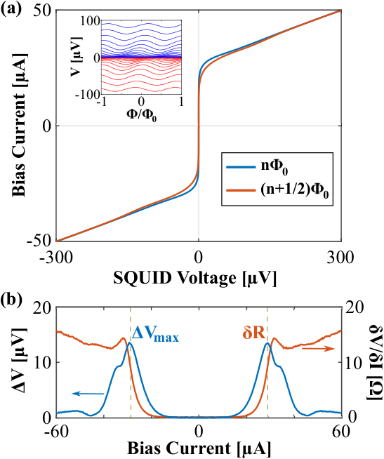
The amplifier input voltage noise contribution to the total white flux noise should moreover be minimized. This contribution is given by , where is the SQUID voltage-to-flux transfer function. is the maximum voltage modulation depth in response to an externally applied magnetic flux (see Fig. 2).
can be approximated by , where and are the critical current modulation depth and the differential resistance at the optimal bias current working point (i.e., where ), respectively. Therefore, a large value of is desirable in order to minimize the contribution of the amplifier voltage input noise to the total flux noise.
In Fig. 2(a) we show the current voltage characteristics of SQUID SQ2 (see Table 1 for details) measured at K for two different applied magnetic flux values. The shape of the current voltage characteristics resembles that of a resistively shunted junction (RSJ). The voltage modulations of SQUID SQ2 as a function of applied magnetic flux are shown in the inset of Fig. 2(a). Here each curve corresponds to an increment of bias current, , by A. From this measurement one can extract the voltage modulation depth as a function of the bias current, which is shown in Fig. 2(b). From the maximum voltage modulation depth V we obtain for the transfer function at K. This is a net improvement compared to nanowire-based SQUIDs with similar SQUID loop size Xie et al. 2017, which is attributed to the increased differential resistance and reduced parasitic inductance of GDBs as compared to bare nanowires. As will be shown below, this results in lower magnetic flux and field noise as well. The values of measured at K for the other SQUIDs are summarized in Table 1.
In Fig. 3 (a), we show the maximum modulation depth of SQUID SQ0 as a function of temperature . In the temperature range between 10 K and 20 K, decreases rapidly with temperature. Increasing the temperature above 20 K up to K causes to further decrease slightly. For temperatures above 55 K we observe an increase of up to K above which the maximum voltage modulation depth goes to zero when reaching the critical temperature of the GDBs, K.

The non-monotonic behavior of can be understood from the temperature dependence of the critical current modulation depth and the differential resistance at the optimal working point, which are shown in Fig. 3(b). The critical current modulation depth decreases with increasing temperature whereas the differential resistance first decreases with temperature until it increases again for temperatures above K. The increase of the differential resistance with temperature is a typical feature of an SNS-like junction. The product , shown in comparison with in Fig. 3(a) (crosses), reproduces nicely the maximum value of measured voltage modulation depth.
In Fig. 3 (c) we show the critical current of device SQ0 as a function of temperature (blue circles). The solid line is the Bardeen expression for the depairing critical current of superconducting nanowires Nawaz et al. 2013; Bardeen 1962: . Here we used K, the critical temperature of the YBCO film. In our previous workNawaz et al. 2013 we have shown that the Bardeen expression properly reproduces the critical current of YBCO nanowires in the full temperature regime. The fact that the critical current of our GDBs can be well fitted by the Bardeen expression for temperatures below K suggests that the GDBs behave like short Dayem bridges at low temperatures. Here the length of the bridge is approximately given by the GDB gap length ( nm) and the thickness is given by the thickness of the remaining superconducting film, , inside the gap buried under the redeposited amorphous YBCO Trabaldo et al. 2019 (see inset Fig. 3(b)). From the typical critical current density of thin YBCO Dayem bridgesArpaia et al. 2017 A/cm2 at 4.2 K, we therefore obtain for the thickness of the superconducting constriction in the GDB nm.
For K the measured critical current, , clearly departs from the temperature dependence of a bare Dayem bridge predicted by the Bardeen expression, . A possible explanation is the weakening of superconductivity in the constriction of the GDB for approaching K, which could also explain the increase of the differential resistance above K. Indeed, in thin ( nm) YBCO films, a clear broadening of the superconducting transition in resistance vs temperature measurements has been observed Arpaia et al. 2017. This broadening can be attributed to a Kosterlitz-Thouless vortex-antivortex pair dissociation transition close to the of the filmBeasley, Mooij, and Orlando 1979; Bartolf et al. 2010. Alternative explanations include thermal activation of vortex-antivortex pairs or vortices overcoming the Bean-Livingston edge barrier.Arpaia et al. 2014b
The magnetic field noise of SQUID-based magnetometers can be obtained from the flux noise as , where (here and are the magnetic flux through the SQUID loop and the externally applied magnetic field, respectively). Due to their small size, bare SQUIDs have extremely small effective areas , resulting in rather large values for . This is a problem that is common to all SQUIDs, but particularly acute for nanoSQUIDs. To improve the magnetic field sensitivity, SQUIDs can be coupled to a much larger pick-up loop.Koelle et al. 1999 We galvanically coupled 32 SQUIDs to a single pick-up loop, which is integrated directly in the EBL design of the sample, without additional fabrication steps. A schematic of the pick-up loop is shown in the inset of Fig. 4. The pick-up loop has lateral sizes of mm mm and line width of mm.
An externally applied magnetic field results in a screening current circulating the loop which results in a phase difference between the weak links . is the SQUID hairpin loop inductance and represents the coupling inductance between SQUID and pick-up loop. This coupling determines the effective area asArzeo et al. 2016 , where and are the effective areas of the SQUID and pick-up loop, respectively. is the inductance of the pick-up loop. To increase , one needs to increase the coupling by increasing . Since a higher SQUID inductance increases the screening factor , in order to obtain the lowest , the value of needs to be optimized. The coupling inductance values of three SQUIDs were measured using a current injection scheme.Johansson et al. 2009 The injection current modulates the phase difference between the two GDBs. From the modulation period of the critical current one can extract the inductance of the hairpin loop . In Table 1 we summarize the values of the coupling inductance of the various SQUIDs measured at K.
The magnetic field sensitivity of three different devices were measured at K in a magnetically shielded room. A commercial Magnicon SEL-1 dc-SQUID electronics Magnicon operated in flux-locked loop and bias reversal ( kHz) mode was used to measure the magnetic flux noise. From the measured magnetic flux noise , the magnetic field noise is calculated as . Here the effective area was separately measured via responsivity measurements using a calibrated Helmholtz coil.Ruffieux et al. 2020
| [nm] | [nm] | [m] | [A] | [pH] | [V] | [mm2] | [] | [] | ||
|---|---|---|---|---|---|---|---|---|---|---|
| SQ0 | 40 | 150 | 8 | 92 | - | - | 30 | - | - | - |
| SQ1 | 50 | 200 | 16 | 15 | 48.5 | 0.3 | 39 | 0.15 | 6 | 85 |
| SQ2 | 50 | 200 | 30 | 30 | 103 | 1.5 | 16.5 | 0.35 | 10.6 | 63 |
| SQ3 | 50 | 200 | 30 | 16 | 103 | 0.8 | 18.7 | 0.35 | 11 | 67 |
In Table 1 we summarize the magnetic noise properties of three different SQUID magnetometers. Devices SQ2 and SQ3 were fabricated on the same chip sharing the same pick-up loop, whereas SQ1 was realized on a different chip. The best performance in terms of voltage modulations and flux noise are achieved on device SQ1. This would be expected given the shorter and, consequently, smaller . However, this also results in a smaller , compared to SQ2 and SQ3, due to reduced coupling. Indeed, devices SQ2 and SQ3, which have larger , show better coupling but at the cost of a reduced . Nevertheless, the of SQ2 and SQ3 results in comparable to state-of-the-art YBCO SQUIDs (, achieved in devices based on grain boundary junctions Öisjöen et al. 2012; Faley et al. 2017; Ruffieux et al. 2020; Chukharkin et al. 2013; Mitchell and Foley 2010; Faley et al. 2014).

The lowest magnetic noise spectral density was achieved for SQ2 and is shown in Fig. 4. The knee is below Hz and the white magnetic field noise is around fT/. This result is almost a factor 2 lower than that which was previously obtained with GDB weak linksTrabaldo et al. 2019 and represents the lowest field noise achieved in SQUID magnetometers implementing Dayem bridge based weak links. Moreover, the measured magnetic field noise is comparable with the lowest reported field noise values achieved with single-layer grain boundary-based SQUIDs galvanically coupled to a pick-up loop made on mm mm substrates Öisjöen et al. 2012; Ruffieux et al. 2020; Faley et al. 2014; Lee et al. 1995; Beyer et al. 1998, fT.
In conclusion, we have studied the temperature dependence of GDB based SQUIDs. At low temperatures, the GDBs behave like short and thin Dayem bridges, whereas at temperatures above 60 K the fluctuation-driven suppression of superconductivity in the constriction of the GDB causes the weak link to behave like an SNS junction. This results in a local maximum in the temperature dependence of the transfer function around 65 K. Magnetic field noise as low as fT/ at K has been obtained for GDB based magnetometers galvanically coupled to an in-plane pick-up loop. Such low values makes these devices an attractive candidate for magnetoencephalography application, possibly outperforming their LTS counterpart.Riaz, Pfeiffer, and Schneiderman 2017
Acknowledgements.
This work was been supported in part by the Knut and Alice Wallenberg Foundation (KAW) and in part by the Swedish Research Council (VR). This project has received funding from the ATTRACT project funded by the EC under Grant Agreement 777222. R.A. is supported by the Swedish Research Council (VR) under the project 2017-00382. This work was performed in part at Myfab Chalmers.References
- Weinstock (2012) H. Weinstock, SQUID sensors: fundamentals, fabrication and applications, Vol. 329 (Springer Science & Business Media, 2012).
- Fagaly (2006) R. Fagaly, “Superconducting quantum interference device instruments and applications,” Review of scientific instruments 77, 101101 (2006).
- Clarke and Braginski (2006) J. Clarke and A. Braginski, “The squid handbook: Applications of squids and squid systems. vol. 2,” (2006).
- Seidel (2015) P. Seidel, Applied Superconductivity: Handbook on Devices and Applications (John Wiley & Sons, 2015).
- Clarke, Lee, and Schneiderman (2018) J. Clarke, Y.-H. Lee, and J. Schneiderman, “Focus on squids in biomagnetism,” Superconductor Sci. Technol. 31, 080201 (2018).
- Granata and Vettoliere (2016) C. Granata and A. Vettoliere, “Nano superconducting quantum interference device: A powerful tool for nanoscale investigations,” Phys. Rep. 614, 1–69 (2016).
- Hilgenkamp and Mannhart (2002) H. Hilgenkamp and J. Mannhart, “Grain boundaries in high-t c superconductors,” Reviews of Modern Physics 74, 485 (2002).
- Koelle et al. (1999) D. Koelle, R. Kleiner, F. Ludwig, E. Dantsker, and J. Clarke, “High-transition-temperature superconducting quantum interference devices,” Reviews of Modern Physics 71, 631 (1999).
- Martínez-Pérez and Koelle (2016) M. J. Martínez-Pérez and D. Koelle, “Nanosquids: Basics & recent advances,” Phys. Sci. Rev. 2 (2016).
- Tafuri and Kirtley (2005) F. Tafuri and J. R. Kirtley, “Weak links in high critical temperature superconductors,” Reports on Progress in Physics 68, 2573 (2005).
- Cho et al. (2018) E. Y. Cho, Y. W. Zhou, J. Y. Cho, and S. A. Cybart, “Superconducting nano josephson junctions patterned with a focused helium ion beam,” Applied Physics Letters 113, 022604 (2018).
- Faley et al. (2014) M. Faley, D. Meertens, U. Poppe, and R. Dunin-Borkowski, “Graphoepitaxial high-tc squids,” in Journal of Physics: Conference Series, Vol. 507 (IOP Publishing, 2014) p. 042009.
- Mitchell and Foley (2010) E. Mitchell and C. Foley, “Ybco step-edge junctions with high icrn,” Supercond. Sci. Technol. 23, 065007 (2010).
- Öisjöen et al. (2012) F. Öisjöen, J. F. Schneiderman, G. Figueras, M. Chukharkin, A. Kalabukhov, A. Hedström, M. Elam, and D. Winkler, “High-t c superconducting quantum interference device recordings of spontaneous brain activity: Towards high-t c magnetoencephalography,” Appl. Phys. Lett. 100, 132601 (2012).
- Nagel et al. (2010) J. Nagel, K. Konovalenko, M. Kemmler, M. Turad, R. Werner, E. Kleisz, S. Menzel, R. Klingeler, B. Büchner, R. Kleiner, et al., “Resistively shunted yba2cu3o7 grain boundary junctions and low-noise squids patterned by a focused ion beam down to 80 nm linewidth,” Superconductor Science and Technology 24, 015015 (2010).
- Beyer et al. (1998) J. Beyer, D. Drung, F. Ludwig, T. Minotani, and K. Enpuku, “Low-noise yba 2 cu 3 o 7- x single layer dc superconducting quantum interference device (squid) magnetometer based on bicrystal junctions with 30∘ misorientation angle,” Applied physics letters 72, 203–205 (1998).
- Foley (1999) C. Foley, “Fabrication and characterisation of ybco single grain boundary step edge junctions,” IEEE Trans. Appl. Supercond. 9, 4281–4284 (1999).
- Trabaldo et al. (2019) E. Trabaldo, C. Pfeiffer, E. Andersson, R. Arpaia, A. Kalaboukhov, D. Winkler, F. Lombardi, and T. Bauch, “Grooved dayem nanobridges as building blocks of high-performance yba2cu3o7- squid magnetometers,” Nano letters 19, 1902–1907 (2019).
- Arpaia et al. (2018) R. Arpaia, E. Andersson, E. Trabaldo, T. Bauch, and F. Lombardi, “Probing the phase diagram of cuprates with yba2cu3o7-δ thin films and nanowires,” Phys. Rev. Mater. 2, 024804 (2018).
- Baghdadi et al. (2015a) R. Baghdadi, R. Arpaia, T. Bauch, and F. Lombardi, “Toward yba2cu3o7-δ nanoscale structures for hybrid devices,” IEEE Trans. Appl. Supercond. 25, 1100104 (2015a).
- Nawaz et al. (2013) S. Nawaz, R. Arpaia, T. Bauch, and F. Lombardi, “Approaching the theoretical depairing current in yba2cu3o7- x nanowires,” Physica C Supercond 495, 33–38 (2013).
- Arpaia et al. (2016) R. Arpaia, M. Arzeo, R. Baghdadi, E. Trabaldo, F. Lombardi, and T. Bauch, “Improved noise performance of ultrathin ybco dayem bridge nanosquids,” Supercond. Sci. Technol. 30, 014008 (2016).
- Trabaldo et al. (2017) E. Trabaldo, M. Arzeo, R. Arpaia, R. Baghdadi, E. Andersson, F. Lombardi, and T. Bauch, “Noise properties of ybco nanostructures,” IEEE Trans. Appl. Supercond. 27 (2017).
- Manos and Flamm (1989) D. M. Manos and D. L. Flamm, Plasma etching: an introduction (Elsevier, 1989).
- Baghdadi et al. (2015b) R. Baghdadi, R. Arpaia, S. Charpentier, D. Golubev, T. Bauch, and F. Lombardi, “Fabricating nanogaps in yba 2 cu 3 o 7- for hybrid proximity-based josephson junctions,” Physical Review Applied 4, 014022 (2015b).
- Granata et al. (2013) C. Granata, A. Vettoliere, R. Russo, M. Fretto, N. De Leo, and V. Lacquaniti, “Three-dimensional spin nanosensor based on reliable tunnel josephson nano-junctions for nanomagnetism investigations,” Appl. Phys. Lett. 103, 102602 (2013).
- Xie et al. (2017) M. Xie, M. Chukharkin, S. Ruffieux, J. Schneiderman, A. Kalabukhov, M. Arzeo, T. Bauch, F. Lombardi, and D. Winkler, “Improved coupling of nanowire-based high-t c squid magnetometers—simulations and experiments,” Supercond. Sci. Tech. 30, 115014 (2017).
- Tesche and Clarke (1977) C. D. Tesche and J. Clarke, “dc squid: Noise and optimization,” Journal of Low Temperature Physics 29, 301–331 (1977).
- Arpaia et al. (2014a) R. Arpaia, M. Arzeo, S. Nawaz, S. Charpentier, F. Lombardi, and T. Bauch, “Ultra low noise yba2cu3o7- nano superconducting quantum interference devices implementing nanowires,” Appl. Phys. Lett. 104, 072603 (2014a).
- Bardeen (1962) J. Bardeen, “Critical fields and currents in superconductors,” Reviews of modern physics 34, 667 (1962).
- Arpaia et al. (2017) R. Arpaia, D. Golubev, R. Baghdadi, R. Ciancio, G. Dražić, P. Orgiani, D. Montemurro, T. Bauch, and F. Lombardi, “Transport properties of ultrathin yba 2 cu 3 o 7- nanowires: A route to single-photon detection,” Physical Review B 96, 064525 (2017).
- Beasley, Mooij, and Orlando (1979) M. Beasley, J. Mooij, and T. Orlando, “Possibility of vortex-antivortex pair dissociation in two-dimensional superconductors,” Physical Review Letters 42, 1165 (1979).
- Bartolf et al. (2010) H. Bartolf, A. Engel, A. Schilling, K. Il’In, M. Siegel, H.-W. Hübers, and A. Semenov, “Current-assisted thermally activated flux liberation in ultrathin nanopatterned nbn superconducting meander structures,” Physical Review B 81, 024502 (2010).
- Arpaia et al. (2014b) R. Arpaia, D. Golubev, R. Baghdadi, M. Arzeo, G. Kunakova, S. Charpentier, S. Nawaz, F. Lombardi, and T. Bauch, “Resistive state triggered by vortex entry in yba2cu3o7- nanostructures,” Physica C: Superconductivity and its Applications 506, 165–168 (2014b).
- Arzeo et al. (2016) M. Arzeo, R. Arpaia, R. Baghdadi, F. Lombardi, and T. Bauch, “Toward ultra high magnetic field sensitivity yb a 2 c u 3 o 7- nanowire based superconducting quantum interference devices,” J. Appl. Phys. 119, 174501 (2016).
- Johansson et al. (2009) J. Johansson, K. Cedergren, T. Bauch, and F. Lombardi, “Properties of inductance and magnetic penetration depth in (103)-oriented yba 2 cu 3 o 7- thin films,” Phys. Rev. B 79, 214513 (2009).
- (37) Magnicon, SQUID electronics SEL-1, http://www.magnicon.com.
- Ruffieux et al. (2020) S. Ruffieux, A. Kalaboukhov, M. Xie, M. Chukharkin, C. Pfeiffer, S. Sepehri, J. F. Schneiderman, and D. Winkler, “The role of kinetic inductance on the performance of ybco squid magnetometers,” Superconductor Science and Technology 33, 025007 (2020).
- Faley et al. (2017) M. Faley, J. Dammers, Y. Maslennikov, J. Schneiderman, D. Winkler, V. Koshelets, N. Shah, and R. Dunin-Borkowski, “High-tc squid biomagnetometers,” Superconductor Science and Technology 30, 083001 (2017).
- Chukharkin et al. (2013) M. Chukharkin, A. Kalabukhov, J. F. Schneiderman, F. Öisjöen, M. Jönsson, M. Xie, O. V. Snigirev, and D. Winkler, “Improvement of ultra-low field magnetic resonance recordings with a multilayer flux-transformer-based high-tc squid magnetometer,” IEEE Trans. Appl. Supercond. 23 (2013).
- Lee et al. (1995) L. Lee, J. Longo, V. Vinetskiy, and R. Cantor, “Low-noise yba2cu3o7- direct-current superconducting quantum interference device magnetometer with direct signal injection,” Applied physics letters 66, 1539–1541 (1995).
- Riaz, Pfeiffer, and Schneiderman (2017) B. Riaz, C. Pfeiffer, and J. F. Schneiderman, “Evaluation of realistic layouts for next generation on-scalp meg: spatial information density maps,” Sci. Rep. 7, 6974 (2017).