Orbital Hall Insulating Phase in Transition Metal Dichalcogenide Monolayers
Abstract
We show that H-phase transition metal dichalcogenides (TMDs) monolayers such as MoS2 and WSe2, are orbital Hall insulators. They present very large orbital Hall conductivity plateaus in their semiconducting gap, where the spin Hall conductivity vanishes. Our results open the possibility of using TMDs for orbital current injection and orbital torque transfers that surpass their spin-counterparts in spin-orbitronics devices. The orbital Hall effect (OHE) in TMD monolayers occurs even in the absence of spin-orbit coupling. It can be linked to exotic momentum-space Dresselhaus-like orbital textures, analogous to the spin-momentum locking in 2D Dirac fermions that arise from a combination of orbital attributes and lattice symmetry.
The flexibility to combine atom-thick layers with different characteristics in novel quantum metamaterials makes two-dimensional (2D) systems interesting platforms for spintronics Han et al. 2014; Avsar et al. 2019. In recent years, innovative routes to generate and manipulate spin currents in 2D materials where spin-orbit coupling mediates the conversion between charge and spin currents have been discovered, such as the spin Hall effect (SHE), Rashba-Edelstein effect (REE) Offidani et al. 2017 and all-optical spin injection Avsar et al. 2017. Orbital angular momentum can be manipulated like spin and be relevant in many materials, even in the absence of strong spin-orbit coupling (SOC). Orbitronics, an analog of spintronics that operates with the electronic orbital angular momentum degrees of freedom, although embryonic, is sparking renewed interests. An increasing number of effects are being predicted, such as the orbital-momentum locking Castro de Lima et al. 2019, orbital torque Go and Lee 2020, orbital Rashba effect Go et al. 2017; Park et al. 2013; Park et al. 2012, orbital Edelstein effect Yoda et al. 2018; Salemi et al. 2019 and orbital Hall effect (OHE) Bernevig et al. 2005; Tanaka et al. 2008, an orbital analog of the SHE.
The OHE, similarly to the SHE, refers to the creation of a transverse flow of orbital angular momentum (OAM) that is induced by a longitudinally applied electric field Bernevig et al. 2005. It has been explored mostly in three dimensional metallic systems, where it can be quite strong Tanaka et al. 2008; Kontani et al. 2008; Kontani et al. 2009; Go et al. 2018. However, the OHE does not necessarily rely on strong SOC. It can be linked to orbital textures Go et al. 2018 where the OAM is locked to the carrier momentum (similar to the spin-momentum locking observed in systems that present REE), and can be relevant in a diverse pool of materials. Recent theoretical results have predicted the existence of OHE in 2D insulators, suggesting that this effect could be found also in other elements of this class of systems Canonico et al. 2020.
Single layers of TMDs hold great appeal for electronics, optoelectronics, and spintronics applications Manzeli et al. 2017; Mak and Shan 2016; Gmitra and Fabian 2015; Cysne et al. 2018a; Cysne et al. 2018b. Two-dimensional layers of TMDs such as MX2 (M =Mo,W,and X =S,Se,Te) exhibit direct band-gap properties that are ideal for optoelectronics applications Mak and Shan 2016. Their lack of inversion symmetry, combined with strong SOC, causes a sizeable spin splitting at the valence band edges, enabling spin- and valley-selective light absorption. These characteristics provide all-optical methods for manipulation of internal degrees of freedoms, enabling, for example, all-optical spin-injection. Although the OAM is present in TMDs and coupled to the valley and spin degrees of freedom, the possibility of manipulating it in TMDs monolayers for spin-orbitronics applications is just beginning to be noticed Xiao et al. 2012; Mak et al. 2018.
Only a few studies of OHE were performed in 2D materials, partially due to their usually small orbital conductivity values Tokatly 2010; Phong et al. 2019; Canonico et al. 2020. The search for 2D materials with a robust orbital signal is fundamental for possible developments in orbitronics. Here, we shall investigate the orbital Hall conductivity of transition metal dichalcogenide (TMD) monolayers in the H structural phase. For this purpose, we first consider a simplified tight-binding (TB) model involving only three relevant orbitals of the transition metal atoms. We then extend our analysis to a more involved multiband TB model that includes the and orbitals of the chalcogen atoms, as well as the orbitals of the TM atoms. The hopping integrals and onsite energies are obtained from ab initio calculations Pizzi et al. 2019. In both cases, we demonstrate that TMDs host very robust orbital Hall currents in their insulating gap, even in the absence of spin-orbit coupling. The orbital Hall conductivity can be significantly larger than the spin Hall one and exhibits a relatively large plateau inside the TMD electronic energy gap, where the SHE is absent.
The atomic environment of the transition metal atoms together with the interaction with the chalcogen atoms lead to a large crystal field splitting. The resulting band edges are well reproduced by a TB model comprising three atomic orbitals only arranged in a triangular lattice. This 3-bands model captures the essential features of the energy spectrum near valleys of most single layer TMD-H Liu et al. 2013. The TB Hamiltonian is given by
| (1) |
Here, and denote the triangular lattice sites positioned at and , respectively. indicates that the sum is restricted to the nearest neighbour (n.n) sites only. The operator creates an electron of spin in the atomic orbitals located at site , where represent the atomic orbitals , and , respectively; is the corresponding on-site atomic energy associated with orbital , and are the transfer integrals between orbitals and centred on sites and , respectively, constructed based on symmetry operations of the point group D3h of TMDs Liu et al. 2013. The third term describes an intrinsic atomic SOC where .
To calculate the orbital-Hall (OH) and spin-Hall (SH) conductivities for the TMDs make use of the Kubo-Bastin formula Bastin et al. 1971:
| (2) |
Here, represents the area of the sample, is the Fermi-Dirac distribution for energy , chemical potential and temperature . symbolises the advanced(retarded) one-electron Green function. To calculate the SH conductivity , we take as the current-density operator component along the applied electric field direction , , and as the transverse spin current-density operator component where is the spin-Pauli’s matrix and is the transverse component of the velocity operator. For calculating the OH conductivity , we consider and as the orbital transverse current density operator component , where is the -component of the atomic angular momentum operator. Eq. (2) is equivalent to the Kubo formula written in terms of spin and orbital Berry curvatures Go et al. 2018; Phong et al. 2019; Sup.
Our transport calculations are performed in real-space with the use of a modified version of the quantum transport software KITE João et al. 2019 based on Chebyshev polynomial expansions Weiße et al. 2006. This method is highly efficient for computation of Hall responses in 2D systems García et al. 2015; Ferreira and Mucciolo 2015; Canonico et al. 2019; Garcia and Rappoport 2016; Garcia et al. 2017. Our simulations were performed for systems with unit cells, including up to 1024 moments in the Chebyshev polynomial expansion


Panels (a) and (c) of Figure 1 show the band structures of MoS2 and WSe2, respectively, both calculated with the 3-bands TB model in the presence of SOC. The SOC causes a splitting in the valence band in the vicinity of the symmetry point, which is clearly more pronounced for WSe2. Panels (b) and (d) exhibit the corresponding spin-Hall, and orbital-Hall conductivities, as well as the densities of states, calculated for MoS2 and WSe2, respectively. As expected, the spin-Hall conductivities for the H-TMDs with SOC vanish in the main energy gap because they are topologically trivial Feng et al. 2012. However, the orbital-Hall conductivities are finite and exhibit plateaus of rather large magnitude within this energy range. We notice that these plateaus have similar values for MoS2 and WSe2, despite the markedly difference in their SOC intensities. In fact, the TMDs display very similar OHE plateaus even in the absence of SOC, as Fig. 2 illustrates. Panel (a) of Fig. 2 shows the band structure of MoS2 calculated using the 3-bands TB model without SOC, and panel (b) depicts the corresponding orbital-Hall conductivity and the density of states.The spin-Hall conductivity in this case is zero and is worthless displaying it. Comparing Figs. 1 (b) and 2 (b), we clearly see that the presence of SOC in the TMDs affects the metallic phase, but just a little the orbital-Hall conductivity plateau. It slightly changes the plateau width by introducing a spin splitting in the valence band around the symmetry point, but the plateau hight is not altered. As we shall subsequently see, this comes from the fact that the accumulated in-plane orbital texture of the occupied states up to top of the valence band remains the same with the introduction of the SOC. One should notice that the OHE is a consequence of the existence of non-trivial angular-momentum-weighted (non-abelian) Berry curvature, as defined in references Phong et al. 2019; Go et al. 2018; Murakami et al. 2003. This curvature can be non-trivial even in the presence of time-reversal and inversion symmetry and can be used as an alternative approach to calculate the OHE.
To get a further insight on the origin of this novel effect, it is instructive to enquire into the nature of the orbital textures in the TMDs, since they are linked to the OHE in three dimensional metals Go et al. 2018 as well as in two-dimensional metals and insulators Canonico et al. 2020. This simplified 3-bands TB model is restricted to a sector of the angular momentum vector space spanned only by the eigenstates of : and associated with , respectively. Within this sector, it is useful to introduce a pseudo angular momentum -algebra. The angular momentum operator components in this basis can be obtained from , imposing that . We can also define the orbital texture associated with each electronic band,
| (3) |
where are the Cartesian unit vectors, represent the eigenstates associated with the energy bands , where label the 3-bands in increasing order of energy and s designate the spin sector.


Let us begin by analysing the orbital angular momentum textures for MoS2 in the absence of spin-orbit coupling. Panels (c), (d) and (e) of Fig.2 illustrates both the out-of-plane (color map) and the in-plane (vector field) projections of the orbital textures, calculated without SOC, for the energy bands , respectively. Panel (c) evinces that the valence bands of TMD monolayers exhibit an orbital-valley locking, showing that this effect precedes the well stablished spin-valley locking in TMDs and takes place even in the absence of SOC. In panel (d) we see that the out-of-plane component for the conduction band vanishes at the valleys. The orbital textures of the valence and conduction bands near and as well as the orbital-valley locking are consistent with experimental optical characterisation of the valley-Zeeman effect in TMD monolayers Stier et al. 2016. Panel (e) also shows orbital-valley locking even in absence of SOC for the highest energy band.
The OHE is caused by the dynamics of the in-plane orbital texture under the influence of an external longitudinal electric field, similarly to the SHE in the presence of Rashba SOC Sinova et al. 2004. It is clear from panels (c), (d) and (e) of Fig. 2 that the in-plane component of the orbital texture is stronger near the () points and thus, the main contribution for the OHE in the insulating phase comes from the valley states where the simplified 3-bands model works pretty well. The contribution from the rest of the BZ affects the OHE quantitatively only. Fig. 2 (b) clearly shows that the OHE exists within the electronic energy band gap even in the absence of SOC. We also have checked that the inclusion of up to three next nearest neighbours hopping integrals in our 3-bands TB model Liu et al. 2013 has a negligible effect on the orbital texture and in the OHE plateau, although it modifies OHE in the metallic phase Sup. The in-plane texture of the valence band near valleys is similar to a Dresselhaus orbital texture found for the - model in honeycomb lattice, which also exhibits OHE in an insulating phase Canonico et al. 2020. When SOC is included the orbital-valley locking persists, as panels (f)-(k) of Fig. 2 show. The in-plane orbital texture is not qualitatively affected by the SOC, but the out-of-plane texture is strongly modified near the point for the conduction band. In its vicinity we find full out-of-plane orbital polarisations with reverse directions for opposite spin sectors. At the and valleys, the out-of-plane orbital texture is again only quantitatively influenced by the SOC, and we see that it has the same signal independent of spin sector. Similarly to what we have previously pointed out, it is the in-plane component of the orbital textures displayed by panels (f)-(k) of Fig. 2 that generates the OHE illustrated in Fig. 1 (b) for MoS2 Canonico et al. 2020.
It is worth mentioning that vertex corrections are not expected to suppress the OHE in the TMDs because of their symmetry Dimitrova 2005, and should not affect the OHE plateau due to the absence of Fermi-surface in insulators Milletarì et al. 2017. We also remark that OAM in the insulator phase of the TMDs can be partially transported by well-known edge-states of TMDs in zigzag nanoribbons Rostami et al. 2016, but additional contributions may come from the bulk Phong et al. 2019.


So far we have used a simplified 3-bands model for unveiling the main features of the OH insulator phase of the TMDs. This model describes very well the physics near valleys, which are responsible for the main contribution to the OHE plateau, and give us good insights about the phenomena. Still, it is crucial to verify if our findings are endorsed by a more realistic calculation that is not restricted to the vicinity of the point. This is especially relevant in this scenario because in a real material other atomic orbitals could contribute to the transport properties of these systems. It is instructive, for example, to inquire into the contributions to the OHE coming from the atomic orbitals of the chalcogen atoms. To this end, we have performed density-functional theory (DFT) calculations, within the local-density approximation (LDA), using the Quantum Espresso numerical packages Giannozzi et al. 2009. We have employed norm-conserving and fully relativistic pseudopotentials Hamann 2013; van Setten et al. 2018, and generated a basis of atomic orbitals using Wannier90 Pizzi et al. 2019 for MoS2, that includes the , , and orbitals of the chalcogen atoms and the five orbitals of the TM atoms (see exact composition of states at in Ref. Molina-Sánchez et al. 2015). The effective tight-binding Hamiltonian obtained with Wannier90 is then exported to KITE, with the help of PythTB scripts Vanderbilt 2018 to carry out our quantum transport calculations. Panels (a) and (c) of Fig. 3 illustrate comparisons between band structure calculations for MoS2 obtained by DFT and by the effective TB Hamiltonian, without and with SOC respectively. We have considered all hopping integrals with energies higher than of the maximum hopping value . The agreement between the two methods is excellent, especially in the vicinity of the band gap.
In panel 3 (b) we present the density of states and OH conductivity calculated with the effective Hamiltonian taking into account 13 orbitals per unit cell, where we see that a sizeable OHE within the MoS2 electronic gap. When SOC is taken into account, a new parametrised Hamiltonian is obtained and we see that it also reproduces the corresponding DFT band structure quite well, including the spin-splitting of the valence band in the vicinity of the Dirac pints - see the inset in panel 3 (b). Figure 3 (d) depict the density of states, SH and OH conductivities calculated with SOC for MoS2. It clearly shows that the OHE is much stronger than the SHE for H-TMDs. The OH plateau height calculated with this full TB parametrisation is approximately 30 smaller than the one obtained with the simplified 3-bands TB model. This seems reasonable because the OHE depends upon details of the electronic structure Canonico et al. 2020 and the OH plateau height increases with the projected Berry curvature value. Since the curvature of the band structure in the vicinity of the Dirac point is more pronounced for the 3-bands model, it is likely to yield a higher plateau. We also note that SOC clearly does not affect much the OHE within the energy gap for the H-TMDs, reinforcing the fact that the OHE is essentially linked to the orbital composition and symmetry of the system.
Regarding the observation of the OH insulating phase, we recall that within the energy gap of the H-TMDs no spin Hall current is generated by a longitudinally applied electric field, but a pure orbital Hall current is produced. In order to detect it we envisage this pure orbital angular momentum current being injected into a suitable system with non negligible SOC, thereby inducing a spin current that can be detected by the inverse SHE in a non-magnetic material or by means of exerted torques on a ferromagnet, as suggested in references Go and Lee 2020 and Zheng et al. 2020.
It is noteworthy that the valley Hall effect (VHE) displayed by TMDs bears similarities with the OHE discussed here, but they are not the same phenomena. The VHE is associated with the valley OAM Mak et al. 2018; Xiao et al. 2010 and requires no sizeable orbital angular momentum texture to occur. It may happen, for example, in graphene when sub-lattice symmetry is broken Ren et al. 2016. In contrast, the OHE is related to the existence of orbital angular momentum textures in reciprocal space, which arise from characteristics of the and atomic orbitals and lattice symmetry. It does not rely on the existence of well-defined valleys and takes place also in systems with indirect band gaps Canonico et al. 2020. When the VHE contribution is written in terms of its OAM Xiao et al. 2007, the total OHE is a sum of the two contributions. Presently, however, it may be experimentally challenging to discriminate them in the TMDs. Careful analysis of their roles in non-local transport experiments Velenzuela and Tinkham 2006 and valley-selective dichroism Xiao et al. 2012; Cao et al. 2012 may possibly lead to progress in this direction, as well as further investigations on orbital and valley angular momentum coherence lengths.
In summary, with quantum transport calculations we have shown that TMDs such as MoS2 and WSe2 are orbital Hall insulators and can host sizeable OHE for energies within their electronic energy gaps. The use of OAM as an information carrier in TMDs widens the development possibilities for novel spin-orbitronics two-dimensional devices.
Acknowledgements.
We acknowledge CNPq/Brazil, CAPES/Brazil, FAPERJ/Brazil and INCT Nanocarbono for financial support, and NACAD/UFRJ for providing high-performance computing facilities. TGR acknowledges COMPETE2020, PORTUGAL2020, FEDER and the Portuguese Foundation for Science and Technology (FCT) through project POCI-01- 0145-FEDER-028114. TPC acknowledges São Paulo Research Foundation (FAPESP) grant 2019/17345-7Supplementary material for “Orbital Hall Insulating Phase in Transition Metal Dichalcogenide Monolayers”
I Kubo formula for linear response conductivity
In the main text, we used the Kubo-Bastin formula to compute spin and orbital Hall conductivities for tight-binding models in real-space. Here we shall briefly examine an alternative formulation for calculating orbital and spin Hall conductivities, which is equivalent to Eq. 2 of the main text. With this approach the spin Hall (SH) and orbital Hall (OH) -polarized response, in direction, to an electric field applied in direction is given by,
| (4) |
| (5) |
where is the orbital Hall (spin Hall) DC conductivity with polarizsation in -direction, is the gauge-invariant spin and orbital weighted Berry curvatures. In Eq. 5, and are eigenvalues and eigenvectors of the tight-binding Hamiltonian in the reciprocal space, for Bloch band, and labels the spin-sector. The velocity operators are defined as , where is the tight-binding Hamiltonian in reciprocal space. The current density operator component in direction is defined as , where for OH (SH) conductivities polarized in direction.
II OHE for 3-bands model using Kubo Formula for MoS2
We have examined the orbital-Hall insulating phase of TMDs by considering a simplified 3-bands model that includes only three atomic orbitals () of the transition metal (TM) atoms arranged in a triangular lattice. The hopping integrals for his effective 3-bands model are computed by assuming the -point group symmetry of the TMD in the H structural phase, which captures the effect of the hybridization of the -orbitals of TM with the -orbitals of the chalcogenes. This effective model was developed by Liu et. al. Liu et al. 2013. As a first approximation, they consider first nearest neighbour hopping integrals only in the triangular lattice. This simplified model was then used to fit the energy spectrum of DFT calculations near the K-points (valleys) of the two dimensional (2D) first Brillouin Zone (BZ). The TB parameters obtained for this simplified model and the corresponding Hamiltonian written in the reciprocal space are registered in reference [Liu et al. 2013].
The representation of the -component of the orbital angular momentum operator in this simplified 3-bands model is given by
| (6) |
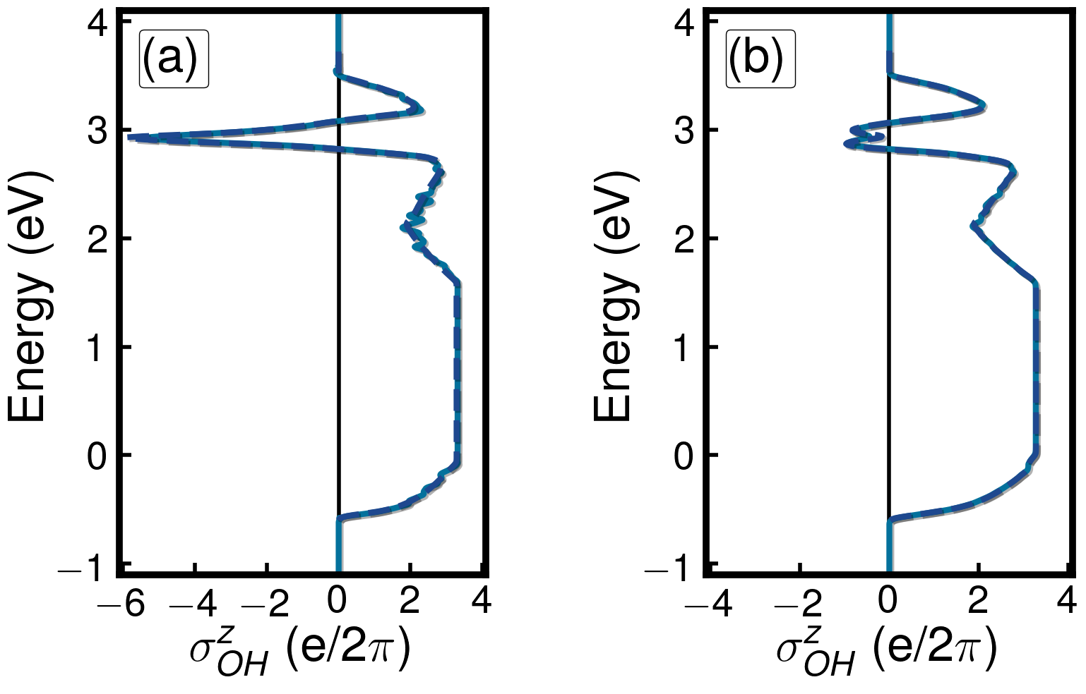
We have mentioned in the main text that the Kubo-Bastin formula used in our primary calculations is equivalent to Eqs. (4) and (5) shown above. In order to illustrate such equivalence we compare results obtained for the orbital Hall conductivity of MoS2 with both approaches. They are depicted in Fig. 4, where the blue solid lines represent the results calculated with the the Kubo-Bastin formula and the black dashed lines the ones obtained with Eqs. (4) and (5). Panels (a) and (b) show the calculated results without and with SOC, respectively. The agreement between the two approaches is excellent, as expected.
As reported in in reference [Liu et al. 2013], the TB parameterization with first nearest-neighbour (1nn) hopping integrals only works well in the vicinity of the -points, but relatively far from them the energy spectrum is not well reproduced. An improvement can be obtained by including up to three nearest-neighbor (3nn) hopping integrals in this model, reproducing very well the band edges, higher energy valence-band () and lower energy conduction-band () in the vicinity of the semiconducting gap obtained by DFT calculations. The detailed construction and the parameters obtained with both first 1nn and up to 3nn approximations can be found also in same reference.
In our work, we have presented results for the OH conductivity calculated with 3-bands TB model taking into account 1nn-hopping integrals only, and mentioned that it gives a good description of the orbital-Hall plateau. Here, we compare results for the OHE calculated for MoS2 with the 3-bands model considering 1nn hopping integrals and up to 3nn. To this end, we used the Kubo-formula given by the Eqs. (4) and (5) of this Supplementary Material (SM) to compute the orbital Hall conductivities employing both approximations.
Figure 5 shows the results for OHE obtained with the 1nn (blue dashed curves) and 3nn (black solid curves) approximations, in the presence (right panel) and in the absence (left panel) of spin-orbit coupling (SOC). It is worth noticing that the OH plateau height changes very little with the inclusion 3nn hopping integrals. This corroborates our reasoning that the OH insulator phase in TMDs is dominated by a Dresselhaus-like orbital-texture [Canonico et al. 2020] near valleys, as mentioned in the main text. The metallic phase, however, is strongly affected by the inclusion of 3nn hopping integrals, as expected. The height of the OH plateau is proportional to the integral of the orbital Berry-curvature in the 2D first BZ. Figure 6 illustrates a density-plot of the orbital Berry-curvature for the valence band , namely , in entire 2D first BZ for MoS2. The results are obtained using the 3-bands model without SOC, taking into account 1nn hopping integrals only (the left panel) and up to 3nn (right panel). Although the orbital-Berry curvatures calculated with 1nn and up to 3nn are very different far from the valleys, the peaks near K-points are very similar - see color code in the figure (6) - leading to almost identical OH plateau heights in both cases.


References
- Han et al. (2014) W. Han, R. Kawakami, M. Gmitra, and J. Fabian, Nature Nanotech 9, 794–807 (2014), URL https://www.nature.com/articles/nnano.2014.214.
- Avsar et al. (2019) A. Avsar, H. Ochoa, F. Guinea, B. Ozyilmaz, B. J. van Wees, and I. J. Vera-Marun, arXiv:1909.09188 (2019), URL https://arxiv.org/abs/1909.09188.
- Offidani et al. (2017) M. Offidani, M. Milletarì, R. Raimondi, and A. Ferreira, Phys. Rev. Lett. 119, 196801 (2017), URL https://link.aps.org/doi/10.1103/PhysRevLett.119.196801.
- Avsar et al. (2017) A. Avsar, D. Unuchek, J. Liu, O. Lopez Sanchez, K. Watanabe, T. Taniguchi, B. Ozyilmaz, and A. Kis, ACS Nano 11, 11678 (2017), URL https://pubs.acs.org/doi/abs/10.1021/acsnano.7b06800.
- Castro de Lima et al. (2019) F. Castro de Lima, G. J. Ferreira, and R. H. Miwa, Nano Lett. 19, 6564 (2019), URL https://pubs.acs.org/doi/abs/10.1021/acs.nanolett.9b02802.
- Go and Lee (2020) D. Go and H.-W. Lee, Phys. Rev. Research 2, 013177 (2020), URL https://link.aps.org/doi/10.1103/PhysRevResearch.2.013177.
- Go et al. (2017) D. Go, J.-P. Hanke, M. P. Buhl, F. Freimuth, G. Bihlmayer, H.-W. Lee, Y. Mokrousov, and S. Blugeç, Scientific Reports 7, 46742 (2017), URL https://www.nature.com/articles/srep46742.
- Park et al. (2013) J.-H. Park, C. H. Kim, H.-W. Lee, and J. H. Han, Phys. Rev. B 87, 041301 (2013), URL https://link.aps.org/doi/10.1103/PhysRevB.87.041301.
- Park et al. (2012) J.-H. Park, C. H. Kim, J.-W. Rhim, and J. H. Han, Phys. Rev. B 85, 195401 (2012), URL https://link.aps.org/doi/10.1103/PhysRevB.85.195401.
- Yoda et al. (2018) T. Yoda, T. Yokoyama, and S. Murakami, Nano Lett. 18, 916 (2018), URL https://pubs.acs.org/doi/abs/10.1021/acs.nanolett.7b04300.
- Salemi et al. (2019) L. Salemi, M. Berritta, A. K. Nandy, and P. M. Oppeneer, arXiv:1905.08279 (2019), URL https://arxiv.org/abs/1905.08279.
- Bernevig et al. (2005) B. A. Bernevig, T. L. Hughes, and S.-C. Zhang, Phys. Rev. Lett. 95, 066601 (2005), URL https://link.aps.org/doi/10.1103/PhysRevLett.95.066601.
- Tanaka et al. (2008) T. Tanaka, H. Kontani, M. Naito, T. Naito, D. S. Hirashima, K. Yamada, and J. Inoue, Phys. Rev. B 77, 165117 (2008), URL https://link.aps.org/doi/10.1103/PhysRevB.77.165117.
- Kontani et al. (2008) H. Kontani, T. Tanaka, D. S. Hirashima, K. Yamada, and J. Inoue, Phys. Rev. Lett. 100, 096601 (2008), URL https://link.aps.org/doi/10.1103/PhysRevLett.100.096601.
- Kontani et al. (2009) H. Kontani, T. Tanaka, D. S. Hirashima, K. Yamada, and J. Inoue, Phys. Rev. Lett. 102, 016601 (2009), URL https://link.aps.org/doi/10.1103/PhysRevLett.102.016601.
- Go et al. (2018) D. Go, D. Jo, C. Kim, and H.-W. Lee, Phys. Rev. Lett. 121, 086602 (2018), URL https://link.aps.org/doi/10.1103/PhysRevLett.121.086602.
- Canonico et al. (2020) L. M. Canonico, T. P. Cysne, T. G. Rappoport, and R. B. Muniz, Phys. Rev. B 101, 075429 (2020), URL https://link.aps.org/doi/10.1103/PhysRevB.101.075429.
- Manzeli et al. (2017) S. Manzeli, D. Ovchinnikov, D. Pasquier, O. V. Yazyev, and A. Kis, Nature Reviews Materials 2 (2017), URL https://doi.org/10.1038/natrevmats.2017.33.
- Mak and Shan (2016) K. F. Mak and J. Shan, Nature Photonics 10, 216 (2016), URL https://doi.org/10.1038/nphoton.2015.282.
- Gmitra and Fabian (2015) M. Gmitra and J. Fabian, Phys. Rev. B 92, 155403 (2015), URL https://link.aps.org/doi/10.1103/PhysRevB.92.155403.
- Cysne et al. (2018a) T. P. Cysne, A. Ferreira, and T. G. Rappoport, Phys. Rev. B 98, 045407 (2018a), URL https://link.aps.org/doi/10.1103/PhysRevB.98.045407.
- Cysne et al. (2018b) T. P. Cysne, J. H. Garcia, A. R. Rocha, and T. G. Rappoport, Phys. Rev. B 97, 085413 (2018b), URL https://link.aps.org/doi/10.1103/PhysRevB.97.085413.
- Xiao et al. (2012) D. Xiao, G.-B. Liu, W. Feng, X. Xu, and W. Yao, Phys. Rev. Lett. 108, 196802 (2012), URL https://link.aps.org/doi/10.1103/PhysRevLett.108.196802.
- Mak et al. (2018) K. F. Mak, D. Xiao, and J. Shan, Nature Photon 12, 451–460 (2018), URL https://www.nature.com/articles/s41566-018-0204-6.
- Tokatly (2010) I. V. Tokatly, Phys. Rev. B 82, 161404 (2010), URL https://link.aps.org/doi/10.1103/PhysRevB.82.161404.
- Phong et al. (2019) V. o. T. Phong, Z. Addison, S. Ahn, H. Min, R. Agarwal, and E. J. Mele, Phys. Rev. Lett. 123, 236403 (2019), URL https://link.aps.org/doi/10.1103/PhysRevLett.123.236403.
- Pizzi et al. (2019) G. Pizzi, V. Vitale, R. Arita, S. Bluegel, F. Freimuth, G. Géranton, M. Gibertini, D. Gresch, C. Johnson, T. Koretsune, et al., Journal of Physics: Condensed Matter (2019), URL http://iopscience.iop.org/10.1088/1361-648X/ab51ff.
- Liu et al. (2013) G.-B. Liu, W.-Y. Shan, Y. Yao, W. Yao, and D. Xiao, Phys. Rev. B 88, 085433 (2013), URL https://link.aps.org/doi/10.1103/PhysRevB.88.085433.
- Bastin et al. (1971) A. Bastin, C. Lewiner, O. Betbeder-matibet, and P. Nozieres, Journal of Physics and Chemistry of Solids 32, 1811 (1971), ISSN 0022-3697, URL http://www.sciencedirect.com/science/article/pii/S0022369771801476.
- (30) (????), supplementary Material, URL XXX.
- João et al. (2019) S. M. João, Miša Anđelković, L. Covaci, T. Rappoport, J. M. P. Lopes, and A. Ferreira, Kite: high-performance quantum transport software (2019), URL https://zenodo.org/record/3245011.
- Weiße et al. (2006) A. Weiße, G. Wellein, A. Alvermann, and H. Fehske, Rev. Mod. Phys. 78, 275 (2006), URL https://link.aps.org/doi/10.1103/RevModPhys.78.275.
- García et al. (2015) J. H. García, L. Covaci, and T. G. Rappoport, Phys. Rev. Lett. 114, 116602 (2015), URL https://link.aps.org/doi/10.1103/PhysRevLett.114.116602.
- Ferreira and Mucciolo (2015) A. Ferreira and E. R. Mucciolo, Phys. Rev. Lett. 115, 106601 (2015), URL https://link.aps.org/doi/10.1103/PhysRevLett.115.106601.
- Canonico et al. (2019) L. M. Canonico, T. G. Rappoport, and R. B. Muniz, Phys. Rev. Lett. 122, 196601 (2019), URL https://link.aps.org/doi/10.1103/PhysRevLett.122.196601.
- Garcia and Rappoport (2016) J. H. Garcia and T. G. Rappoport, 2D Materials 3, 024007 (2016), URL http://stacks.iop.org/2053-1583/3/i=2/a=024007.
- Garcia et al. (2017) J. H. Garcia, A. W. Cummings, and S. Roche, Nano Letters 17, 5078 (2017), pMID: 28715194, URL https://doi.org/10.1021/acs.nanolett.7b02364.
- Feng et al. (2012) W. Feng, Y. Yao, W. Zhu, J. Zhou, W. Yao, and D. Xiao, Phys. Rev. B 86, 165108 (2012), URL https://link.aps.org/doi/10.1103/PhysRevB.86.165108.
- Murakami et al. (2003) S. Murakami, N. Nagaosa, and S.-C. Zhang, Science 301, 1348 (2003), URL https://science.sciencemag.org/content/301/5638/1348.
- Stier et al. (2016) A. V. Stier, K. M. McCreary, B. T. Jonker, J. Kono, and S. A. Crooker, Nature Communications 7, 10643 (2016), ISSN 2041-1723, URL https://doi.org/10.1038/ncomms10643.
- Sinova et al. (2004) J. Sinova, D. Culcer, Q. Niu, N. A. Sinitsyn, T. Jungwirth, and A. H. MacDonald, Phys. Rev. Lett. 92, 126603 (2004), URL https://link.aps.org/doi/10.1103/PhysRevLett.92.126603.
- Dimitrova (2005) O. V. Dimitrova, Phys. Rev. B 71, 245327 (2005), URL https://link.aps.org/doi/10.1103/PhysRevB.71.245327.
- Milletarì et al. (2017) M. Milletarì, M. Offidani, A. Ferreira, and R. Raimondi, Phys. Rev. Lett. 119, 246801 (2017), URL https://link.aps.org/doi/10.1103/PhysRevLett.119.246801.
- Rostami et al. (2016) H. Rostami, R. Asgari, and F. Guinea, Journal of Physics: Condensed Matter 28, 495001 (2016), URL https://doi.org/10.1088%2F0953-8984%2F28%2F49%2F495001.
- Giannozzi et al. (2009) P. Giannozzi, S. Baroni, N. Bonini, M. Calandra, R. Car, C. Cavazzoni, D. Ceresoli, G. L. Chiarotti, M. Cococcioni, I. Dabo, et al., Journal of Physics: Condensed Matter 21, 395502 (2009), URL http://www.quantum-espresso.org.
- Hamann (2013) D. R. Hamann, Physical Review B 88, 085117 (2013), ISSN 1098-0121, URL https://link.aps.org/doi/10.1103/PhysRevB.88.085117.
- van Setten et al. (2018) M. van Setten, M. Giantomassi, E. Bousquet, M. Verstraete, D. Hamann, X. Gonze, and G.-M. Rignanese, Computer Physics Communications 226, 39 (2018), ISSN 0010-4655, URL https://www.sciencedirect.com/science/article/pii/S0010465518300250?via{%}3Dihub.
- Molina-Sánchez et al. (2015) A. Molina-Sánchez, K. Hummer, and L. Wirtz, Surface Science Reports 70, 554 (2015), ISSN 0167-5729, URL http://www.sciencedirect.com/science/article/pii/S016757291500028X.
- Vanderbilt (2018) D. Vanderbilt, The PythTB Package (Cambridge University Press, 2018), p. 327–362.
- Zheng et al. (2020) Z. C. Zheng, Q. X. Guo, D. Jo, D. Go, L. H. Wang, H. C. Chen, W. Yin, X. M. Wang, G. H. Yu, W. He, et al., Phys. Rev. Research 2, 013127 (2020), URL https://link.aps.org/doi/10.1103/PhysRevResearch.2.013127.
- Xiao et al. (2010) D. Xiao, M.-C. Chang, and Q. Niu, Rev. Mod. Phys. 82, 1959 (2010), URL https://link.aps.org/doi/10.1103/RevModPhys.82.1959.
- Ren et al. (2016) Y. Ren, Z. Qiao, and Q. Niu, Reports on Progress in Physics 79, 066501 (2016), URL https://doi.org/10.1088/0034-4885/79/6/066501.
- Xiao et al. (2007) D. Xiao, W. Yao, and Q. Niu, Phys. Rev. Lett. 99, 236809 (2007), URL https://link.aps.org/doi/10.1103/PhysRevLett.99.236809.
- Velenzuela and Tinkham (2006) S. O. Velenzuela and M. Tinkham, Nature 7442, 176 (2006), URL https://www.nature.com/articles/nature04937.
- Cao et al. (2012) T. Cao, G. Wang, W. Han, H. Ye, C. Zhu, J. Shi, Q. Niu, P. Tan, E. Wang, B. Liu, et al., Nature Communications 3 (2012), URL https://doi.org/10.1038/ncomms1882.