Antiferromagnetic and Electric Polarized States in Two-Dimensional Janus Semiconductor Fe2Cl3I3
Abstract
Two-dimensional (2D) Janus semiconductors with mirror asymmetry can introduce novel properties, such as large spin-orbit coupling (SOC) and normal piezoelectric polarization, which have attracted a great interest for their potential applications. Inspired by the recently fabricated 2D ferromagnetic (FM) semiconductor CrI3, a stable 2D (in x-y plane) antiferromagnetic (AFM) Janus semiconductor Fe2Cl3I3 with normal sublattice magnetization () is obtained by density functional theory calculations. By applying a tensile strain, the four magnetic states sequentially occur: AFM with of sublattice, AFM with of sublattice, FM with , and FM with . Such novel magnetic phase diagram driven by strain can be well understood by the spin-spin interactions including the third nearest-neighbor hoppings with the single-ion anisotropy, in which the SOC of I atoms is found to play an essential role. In addition, the electric polarization of Fe2Cl3I3 preserves with strain due to the broken inversion symmetry. Our results predict the rare Janus material Fe2Cl3I3 as an example of 2D semiconductors with both spin and charge polarizations, and reveal the highly sensitive strain-controlled magnetic states and magnetization direction, which highlights the 2D magnetic Janus semiconductor as a new platform to design spintronic materials.
I I. Introduction
Two-dimensional (2D) materials, such as graphene, transition metal dichalcogenides and black phosphorus K. S. Novoselov 2004; Yu2007; Novoselov et al. 2005; Jin et al. 2009; Mak et al. 2010; Li et al. 2014, have attracted tremendous attention due to their excellent electrical, optical and acoustic properties. Although many efforts have been devoted to investigating 2D materials, the 2D semiconductors with intrinsic magnetism are still rare Bonilla et al. 2018; Wang et al. 2016; Long et al. 2017; Zhou et al. 2016; Zheng et al. 2018; Ersan et al. 2019. Recently, the successful synthesis of intrinsic ferromagnetic (FM) semiconductor monolayer CrI3 Huang et al. 2017 and bilayer CrGeTe3 Gong et al. 2017 with the Curie temperature of 45K and 28K, respectively, has attracted much attention on 2D magnetic semiconductors. However, potential applications of these magnets in spintronics, high Curie temperature above room temperature is highly required. In addition, the large magnetic anisotropy is needed to stabilize the magnetism in 2D systems, according to Mermin-Wagner theorem Mermin and Wagner 1966. The large magnetic anisotropy is predicted in the technetium based 2D magnetic semiconductors You et al. 2020. A useful approach to tune magnetism and Curie temperature is by strain Webster and Yan 2018; Huang et al. 2018; Zheng et al. 2019; Dong et al. 2019; Baskurt et al. 2020; Ersan and Sarikurt 2019; Iyikanat et al. 2018; Sarikurt et al. 2018; Vatansever et al. 2019; Shen et al. 2019; Wu et al. 2019, which can be realized by bending flexible substrates, elongating an elastic substrate, exploiting the thermal expansion mismatch and so on Conley et al. 2013; He et al. 2013; Wang et al. 2015; Hui et al. 2013; Plechinger et al. 2015; Castellanos-Gomez et al. 2013; Roldán et al. 2015.The band gap can also be modified by strain. For example, a transition from the direct band gap semiconductor to a metal was proposed to occur in MoS2 monolayer with a tensile strain up to 15 Scalise et al. 2011. The topological properties, such as the Weyl half-semimetal You et al. 2019a and the room-temperature quantum anomalous Hall effect You et al. 2019b are recently proposed in the 2D ferromagnetic semiconductors. Other than FM materials, antiferromagnetic (AFM) spintronics began to take a shape, because AFM materials can not only be used as an assistant material, such as pinning layers to control the magnetization direction of the adjacent ferromagnetic layers, but also can work as a memory Marti et al. 2014; Wadley et al. 2016; Olejník et al. 2018. Furthermore, the spin seebeck effect in antiferromagnets MnF2 has recently been observed in the experiment Wu et al. 2016. Therefore, the investigation of the FM and AFM spintronics becomes necessary and interesting.
Among various 2D materials, the 2D Janus materials are very attractive. Compared to their protypes, Janus materials have broken symmetries, and thus can induce many intriguing properties, such as large spin-orbit coupling (SOC), piezoelectricity, polarization, etc. Yang et al. 2019; Dong et al. 2017; Guo et al. 2017a; Cheng et al. 2013; Yin et al. 2018; Xu et al. 2020; Kandemir et al. 2018. The first graphene-based Janus material was graphone, where the Dirac cone was opened with a small gap and the FM was obtained Zhou et al. 2009. Substituting one sulfur layer with selenium in GaS, the piezoelectric coefficient in Ga2SSe was enhanced as large as four times Guo et al. 2017b. Recently, some magnetic Janus materials such as VSSeZhang et al. 2019a, Cr2I3X3Zhang et al. 2019b; Zhang et al. 2020, and V2Cl3I3Ren et al. 2020 were theoretically studied, and they exhibited interesting properties such as large piezoelectricity and valley polarization, enhanced Cuire temperatures. The 2D Janus material MoSSe Lu et al. 2017; Zhang et al. 2017, which has been successfully synthesized recently, not only has a better hydrogen evolution reaction efficiency, but also possesses the topological and ferroelastic properties Ma et al. 2018 compared with its protype MoS2 monolayer Er et al. 2018.
In this work, by studying 2D Janus materials M2Cl3I3 (M=3 transition metals) on the basis of the crystal of CrI3, we propose a stable 2D magnetic Janus semiconductor Fe2Cl3I3. By means of first-principle calculations, Fe2Cl3I3 was found to be a 2D AFM semiconductor with out-of-plane magnetization () of sublattice. Due to the charge redistribution caused by different electronegativity of Cl and I atoms and the broken inversion symmetry, Fe2Cl3I3 monolayer possesses electrical polarization of about 0.18 eÅ and piezoelectricity of about 4.48 pm/V. By applying biaxial tensile strain up to about 15 on Fe2Cl3I3 monolayer, a novel phase diagram with four magnetic states is found: AFM with out-of-plane magnetization of sublattice, AFM with in-plane magnetization of sublattice, FM with in-plane magnetization, and FM with out-of-plane magnetization. The magnetic phase can be well understood by the spin-spin interactions with single-ion anisotropy term, the latter is mainly determined by the spin-orbit coupling of I atoms. Our results demonstrate a strain-controlled magnetic phases of 2D Janus magnetic semiconductors controlled by strain, and thus suggest a promising way to design functional materials.
II II. Computational Methods
Our first-principles calculations were carried out with the Vienna ab initio simulation package (VASP) based on the density functional theory (DFT) Kresse and Hafner 1993; Kresse and Furthm¨¹ller 1996. The interactions between nuclei and electrons were described by the projector augmented wave (PAW) method Bl?chl 1994, and the generalized gradient approximation (GGA) in the form proposed by Perdew, Burke, and Ernzerhof (PBE) Perdew et al. 1996 was used to describe the electron exchange-correlation functional. In order to prevent the unphysical interlayer interactions, we build a 20Å vacuum. The cutoff energy was set to be 520 eV, and the K-meshes for structure optimization and self-consistent calculations is and -centered Monkhorst-Pack grid Monkhorst and Pack 1976, respectively. The structure optimization of atomic positions and the lattice vectors were done until the maximum force on each atom was less than 0.0001 eV/, and the total energy was converged to 10-8 eV. During the optimization, the conjugate gradient (CG) scheme were employed. To account for the correlation effects of Fe 3d electrons, the GGA + SOC + U (U = 4 eV which is typical for 3d electrons) was used in most of our calculations, and the effect of different U values was also investigated. The phonon frequencies were obtained by the density functional perturbation theory (DFPT) as implemented in the PHONOPY code Togo and Tanaka 2015 using a supercell. And the molecular dynamics (MD) simulations in the canonical (NVT) ensemble were performed in a supercell at 300K with a Nosé thermostat.
III III. Structural, magnetic and electronic properties
III.1 A. Crystal structures and stability
The crystal structure of 2D Janus Fe2Cl3I3 is shown in Fig.1a, where the Fe atoms are sandwiched by two different halogen atomic layers Cl and I. 2D Fe2Cl3I3 with the broken inversion symmetry belongs to the P31m (No.157) space group. Each primitive cell contains one formula units, and the Fe atoms locate in the center of the distorted octahedron consisting of three Cl atoms and three I atoms, and form a honeycomb lattice.

To examine the stability of 2D Fe2Cl3I3, its formation energy was calculated. The formation energy is defined as , where is the energy of the Fe2Cl3I3 monolayer, is the energy of bulk bcc Fe, and are the energies of Cl2 and I2 molecular dimers, respectively. As shown in Table 1, the formation energy of Fe2I3Cl3 is between FeCl3 and FeI3. The negative value of =-7.04 eV per primitive cell indicates an exothermic reaction. Inspired by the successful synthesis of MoSSe in experiments Lu et al. 2017; Zhang et al. 2017, we propose a similar synthetic scheme to fabricate Janus Fe3Cl3I3 as follows
4FeI3 + 3Cl2 2Fe2Cl3I3 + 3I2,
where the energy difference between products (Fe2Cl3I3, I2) and reactants (FeI3, Cl2) was -5.33 eV, and the negative value suggests the feasibility of this synthetic scheme.
The phonon spectra of Fe2Cl3I3 monolayer were calculated as shown in Fig.1c, where no imaginary frequency mode in the whole Brillouin zone indicates that Fe2Cl3I3 monolayer is dynamically stable. Moreover, after 6ps MD simulation with a time step of 3fs as shown in Fig.1d, no structural changes occur, and Fe2Cl3I3 still keeps a honeycomb lattice, revealing the thermal stability of Fe2Cl3I3. The optimized lattice constant is 6.717Å. To investigate the mechanical property of monolayer Fe2Cl3I3, the Young’s modulus was calculated to be 11.4 N/m, which is much smaller than that of MoS2 (180 N/m) Bertolazzi et al. 2011 and graphene (342 N/m) Politano and Chiarello 2015; Lee et al. 2008, and MoS2 and graphene could suffer from 11% and 13% strain, respectively. The lower Young’s modulus indicates the possible applications of Fe2Cl3I3 monolayer under a larger tensile strain Bertolazzi et al. 2011. Moreover, the formation energy of Fe2Cl3I3 as a function of applied strain, which is defined as is shown in Fig.1e. One may see that it changes continuously from compressed strain (-5) to tensile strain (15) and keeps negative values, revealing the stability of Fe2Cl3I3 under the applied strain.
| Fe2Cl3I3 | FeCl3 | FeI3 | |
|---|---|---|---|
| Ef | -7.04 | -8.89 | -4.37 |
III.2 B. Antiferromagnetic ground state
The magnetic ground state of Fe2Cl3I3 was studied by comparing the total energy of different spin configurations: FM, Néel AFM, stripy AFM, zigzag AFM and paramagnetic (PM) configurations. Table 2 lists the total energy per Fe2Cl3I3 unit cell relative to the ground states. In contrary to FeCl3 and FeI3 monolayers, which possess FM ground state as shown in Table 3, Fe2Cl3I3 has the ground state of zigzag AFM with out-of-plane magnetization. The energy difference between the ground state and the zigzag AFM with in-plane magnetization of sublattice is about 3.7 meV.
| Zigzag AFM() Zigzag AFM() Zigzag AFM() |
| 0.0 3.7 7.5 |
| Néel AFM() Stripy AFM() FM() PM |
| 20.1 19.3 68.9 472.1 |
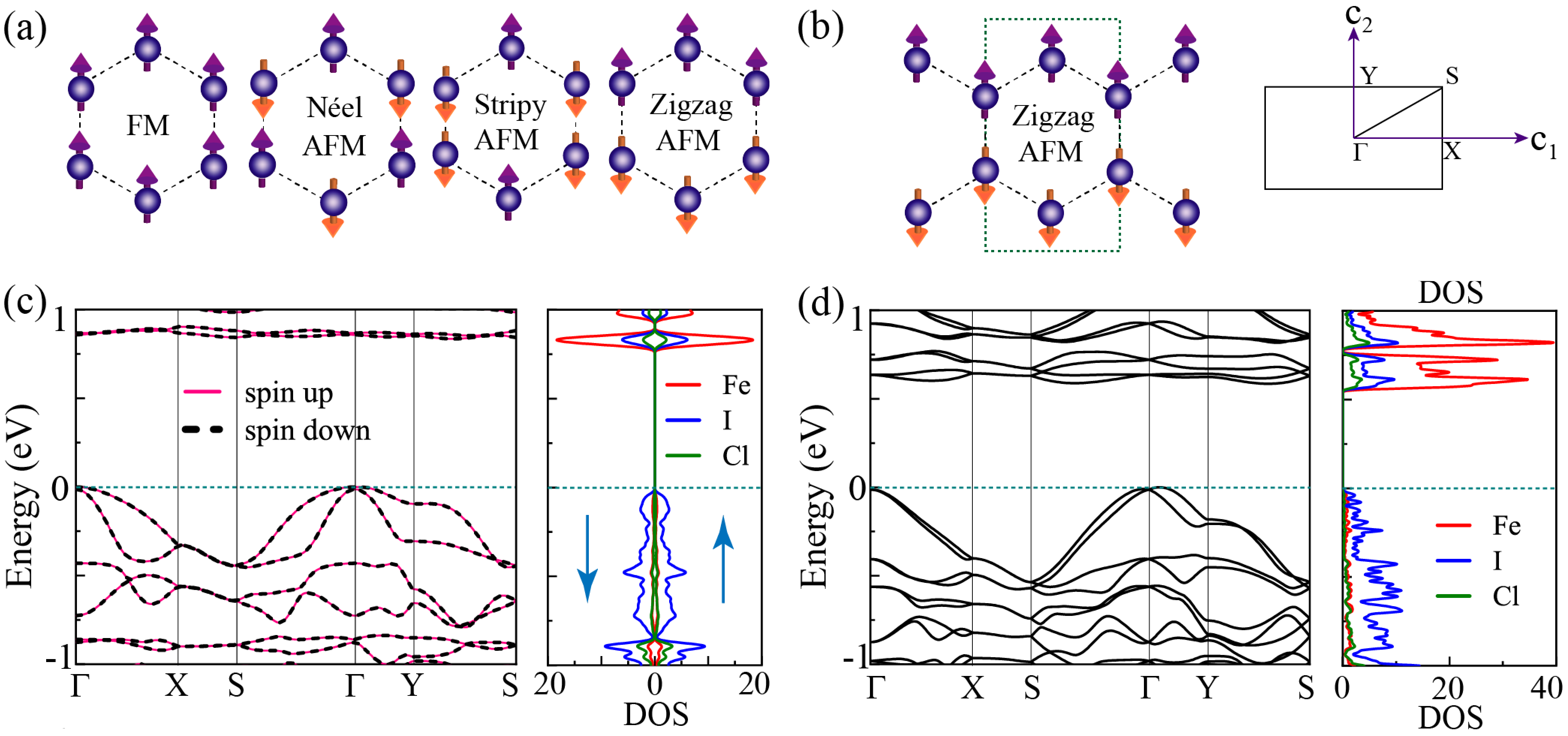
III.3 C. Band structure and Electric polarization
The band structures as well as atom-projected density of states (DOS) of Fe2Cl3I3 calculated by GGA + U and GGA + SOC + U (U = 4 eV) are shown in Fig.2c and Fig.2d, respectively. There is a large difference between the band structures with and without SOC, where a large SOC effect can be expected in Janus materials due to the breaking of inversion symmetry. Without SOC, Fe2Cl3I3 has an indirect band gap of about 0.83 eV. With including SOC, the band gap decreases to about 0.58 eV. The atom-projected DOS shows that the valence and conduction bands near Fermi level are mainly contributed by I and Fe atoms, respectively. Due to the different electronegativity of Cl and I atoms, the charge redistributes. According to the Bader charge analysis, one I atom gains 0.29 e from the Fe atom, and one Cl atom gains 0.55 e from the Fe atom. So a spontaneous electric polarization along the direction perpendicular to the plane with magnitude of 0.18 eÅ was obtained. Thus, the 2D Janus material Fe2Cl3I3 is a rare example of the 2D semiconductors with both spin and charge polarizations.
III.4 D. Effect of strain
The effects of biaxial strain from compress 5 to tensile 15 on the properties of 2D Janus material Fe2Cl3I3 are explored. The magnetic anisotropy energy (MAE) defined as the energy difference between the states with in-plane and out-of-plane spin configurations, E defined as energy difference between the FM and AFM, and the band gap and electric polarization as a function of the strain were plotted in Fig.3. From Fig.3a, it is noted that, E decreases as the increase of tensile strain, and a phase transition from zigzag AFM to FM occurs with the tensile strain of 7. Meanwhile, one can observe that MAE changes from positive to negative, and then returns to the positive value, corresponding to the change of magnetization direction from out-of-plane to in-plane, and then back to out-of-plane. The magnetic ground state changed with the strain can be briefly summarized as four steps: zigzag AFM with out-of-plane magnetization of sublattice, zigzag AFM with in-plane magnetization of sublattice, FM with in-plane magnetization, and FM with out-of-plane magnetization. In addition, the magnetic ground states, MAE and band gaps for Fe2Cl3I3, FeCl3 and FeI3 are shown in Table 3. It can be observed that the formation energy and band gap of Fe2Cl3I3 lie between those of FeCl3 and FeI3, while the magnetic states of these three materials are quite different. Fe2Cl3I3 has a zigzag AFM ground state with out-of-plane sublattice magnetization, FeCl3 has a FM ground state with out-of-plane magnetization, and FeI3 has a FM ground state with in-plane magnetization. On the other hand, the band gap and electric polarization as a function of strain for Fe2Cl3I3 are calculated by GGA + SOC + U (U = 4 eV) as shown in Fig.3b. The band gap and electric polarization preserve with the applied strain. It is interesting to note that as the strain can induce the magnetic phase transition from zigzag AFM to FM phase, the positions of the top of valence band and the bottom of conduction band change under different strains as shown in Fig.4. The strain can change the overlap and hybridization of atomic orbitals, which could lead to change of the electronic band structures. Fe2Cl3I3 in our paper shows the strain-induced magnetic phase transition between antiferromagnetic ground state and ferromagnetic ground state, and the strain-induced change of electronic band structure between indirect and direct band gap. These strain-induced novel magnetic and electronic properties have not been reported in previous studies of the magnetic Janus materials VSSeZhang et al. 2019a, Cr2I3X3Zhang et al. 2019b; Zhang et al. 2020, V2Cl3I3Ren et al. 2020. Moreover, the change of band gap in Fig.3b shows the discontinuity at tensile strain of 10, where a magnetic phase transition occurs from in-plane to out-of-plane ferromagnetization.
To achieve the strain effect on two-dimensional Fe2Cl3I3, we could place Fe2Cl3I3 on a two-dimensional substrate, such as MoS2, h-BN and so on. Once a Fe2Cl3I3 primitive cell matches with a MoS2 cell, whose lattice constant is about 6.36Å, a compressive strain about 5% is applied. Fe2Cl3I3 will retain the zigzag antiferromagnetic ground state, and the magnetic anisotropy and Néel temperature will be enhanced. When we match a Fe2Cl3I3 primitive cell with a h-BN cell, there will be a tensile strain about 12%, and Fe2Cl3I3 will change to a ferromagnetic ground state.
| Magnetic ground state | MAE | Gap | |
|---|---|---|---|
| Fe2Cl3I3 | Zigzag AFM () | 3.7 | 0.58 |
| FeCl3 | FM () | 0.2 | 1.87 |
| FeI3 | FM () | -2.4 | 0.49 |


IV Theoretical Analysis
To better understand the strain-controlled magnetic phase transition in Fe2Cl3I3, we employed a Hamiltonian which can be written as
| (1) |
| (2) |
| (3) |
where H0 includes the spin-spin interaction and H1 contains the single-ion anisotropy. is the spin operator at the i-th lattice site. J1, J2 and J3 are the nearest-neighbor, next nearest-neighbor and third nearest-neighbor exchange integrals, respectively. represents the amplitude of single-ion anisotropy along direction, and is the component of the i-th spin operators. Considering the spin-spin interactions are much larger than single-ion anisotropic energies, for simplicity we ignore the single-ion anisotropy when we estimate J1, J2, and J3 parameters based on DFT results. Although more precise values of exchange parameters in magnetic metals can be obtained using the spin-wave stiffness method Liechtenstein et al. 1987, considering the complicated spin-wave behaviors of H0 with three exchange parameters J1, J2, and J3 for the magnetic semiconductor Fe2Cl3I3, it is not readily to estimate these parameters by means of this method. For simplicity, we opt to use the simple method of energy mapping to estimate the exchange parameters J1, J2 and J3, as many previous works did Sarikurt et al. 2018; Vatansever et al. 2019; Shen et al. 2019; Sivadas et al. 2015; Xiang et al. 2013; Xu et al. 2018. This method can also be adopted to interpret the strain-induced phase transition from AFM to FM in the 2D magnetic semiconductor CrSiTe3 Sivadas et al. 2015. In order to obtain J1, J2 and J3, the energies corresponding to four different magnetic configurations: FM, Nel AFM, stripy AFM and zigzag AFM were expressed as
| (4) | ||||
where E0 is the energy that is independent of spin configurations. Thus, the magnetic phase diagram with respect to J1/J2 and J3/J2 can be obtained by comparing the energies determined by Eq.(4) for a given set of exchange parameters, as shown in Fig. 5. On the other hand, from the DFT results of Fe2Cl3I3 with different strains, the parameters J1, J2, and J3 can be estimated as marked with stars in Fig.5, where the digital numbers of each star denote the corresponding strain.

As shown in Fig.5, Fe2Cl3I3 locate at the zigzag AFM and FM phases. In the FM phase, the magnitude of exchange parameter J1 is much larger than that of J2 and J3, and the model Hamiltonian in Eq.(2) is simplified to the spin-spin interactions with nearest-neighbor coupling J1. While in the zigzag AFM phase, both J1, J2 and J3 are important. Although the jump of digital numbers in the phase diagram correspond to four different magnetic ground states, the phase diagram is obtained from the spin-spin interactions, and can not explain the change of the magnetization directions.
Based on the above magnetic exchange parameters J1, J2 and J3, and keeping the Ising-type interactions in Eq.(2) for simplicity, we use Monte Carlo simulations to estimate the Curie temperature of Janus Fe2Cl3I3 with different biaxial strain. Monte Carlo simulations are performed in a 60601 2D honeycomb lattice with 106 steps for each temperature calculations. As shown in Fig.6, for the zigzag AFM ground states, the Nel temperature decreases from 142K to 33K as the strain changes from -5% to 5%. And when the strain changes from 10% to 15%, the Curie temperature for the corresponding FM ground states with out-of-plane magnetization increases from 65K to 193K. As expected, the critical temperature decreases as the magnetic ground state approaches to the magnetic phase transition boundary driven by strain.

In order to understand the change of magnetization direction, i.e. the sign of MAE in Fig. 3a, we consider the single-ion anisotropy (SIA) term as shown in Eq.(3). According to the second-order perturbation theory, the MAE caused by SIA can be described by sheng Wang et al. 1993; Yang et al. 2017
| (5) |
where is the SOC constant, represents the angular momentum operator, and are the wavefunctions of unoccupied and occupied states, respectively, and and are the corresponding energy levels. A positive value of indicates the out-of-plane magnetization, and negative value indicates the in-plane magnetization.

To unveil the mechanism that leads to the change of with different strains, we have calculated the orbital-resolved . As an example, the orbital-resolved of Fe2Cl3I3 with 8 and 15 tensile strains, which correspond to FM with magnetization along the x-axis and FM with magnetization along the z-axis ground states, respectively, was calculated as shown in Fig.7. By DFT calculations,the main contribution to is from Fe and I atoms, and I atoms can be classified to two kinds as labeled in Fig.7a according to their different surroundings when the magnetization is along the x-axis. In the case of 8 tensile strain, as shown in Table 4, the contributions to from Fe and two kinds of I atoms are -1.2, 2.5 and -4.1 meV, respectively, giving rise to a total negative of -2.8 meV. It is consistent with the in-plane magnetization. For the case of 15 tensile strain, a positive value of 5.3 meV is obtained, which indicates the out-of-plane magnetization. From Fig.7, one may observe that mainly originates from (,), (,) and (,) matrix element of I atoms. As the tensile strain increases from 8 to 15, the sign change of from I atoms gives rise to the sign change of the total , and thus induces the changes of the magnetization direction.
| Fe-d | I1-p | I2-p | Total | |
|---|---|---|---|---|
| 8 | -1.2 | 2.5 | -4.1 | -2.8 |
| 15 | -2.1 | 6.8 | 0.6 | 4.1 |
V Effect of electronic correlation
The electronic correlation effect is important for orbitals in transition-metal compounds, so our above DFT calculations are carried out with = 4 eV. In order to examine the influence of different values on the magnetic ground states, we have studied the magnetic sate of Fe2Cl3I3 for the cases without strain and with 15 tensile strain with parameter from 2 to 5 eV. As shown in Fig.8, when there is no strain applied, with the increase of value, although MAE increases and E decreases, the signs of both preserve, indicating the unchanged AFM ground state with out-of-plane magnetization of sublattice. Similarly, the FM ground state along z-axis magnetization with 15 strain is not changed when different values are employed. Thus, our results about the magnetic phase transition with respect to the strain are robust against values.

VI Conclusion
By first-principles calculations, we have proposed a new 2D magnetic Janus semiconductor–Fe2Cl3I3. which was revealed to exhibit the zigzag AFM ground state with out-of-plane magnetic direction. In contrast to non-Janus materials, the inversion symmetry breaking usually occurs in Janus materials. This can induce the intrinsic electric polarization and enhanced spin-orbital coupling. Fe2Cl3I3 was found to possess a spontaneous polarization along the z-axis. Furthermore, we have also investigated the effect of biaxial strain on the ground state properties of Fe2Cl3I3, and a magnetic phase transition including the antiferromagnetic-ferromagnetic transition and the change of magnetization direction was obtained. Both magnetic and electric polarization were observed in Fe2Cl3I3 under the biaxial strain. A phase diagram based on the spin-spin interactions with the single-ion anisotropy term was proposed to interpret the magnetic phase transition. Our findings not only expose a new stable 2D magnetic Janus semiconductor, but also reveal the highly sensitive strain-controlled magnetic states, and thus highlight the 2D magnetic Janus semiconductor as a new platform to design spintronic materials.
VII Acknowledgements
The authors thank Peng Fan for valuable discussions on the Monte Carlo simulation. This work is supported in part by the National Key RD Program of China (Grant No. 2018YFA0305800), the Strategic Priority Research Program of Chinese Academy of Sciences (Grant No. XDB28000000), the National Natural Science Foundation of China (Grant No. 11834014), and Beijing Municipal Science and Technology Commission (Grant No. Z191100007219013). B.G. is also supported in part by the National Natural Science Foundation of China (Grant No. Y81Z01A1A9), the Chinese Academy of Sciences (Grant No. Y929013EA2), the University of Chinese Academy of Sciences (Grant No.110200M208), the Strategic Priority Research Program of Chinese Academy of Sciences (Grant No.XDB33000000), and the Beijing Natural Science Foundation(Grant No. Z190011).
Zhen Zhang and Jing-Yang You contributed equally to this work.
References
- K. S. Novoselov (2004) S. V. M. D. J. Y. Z. S. V. D. I. V. G. A. A. F. K. S. Novoselov, A. K. Geim, Science 306, 666 (2004).
- Novoselov et al. (2005) K. S. Novoselov, D. Jiang, F. Schedin, T. J. Booth, V. V. Khotkevich, S. V. Morozov, and A. K. Geim, Proc.? Natl.? Acad. ?Sci.? USA 102, 10451 (2005).
- Jin et al. (2009) C. Jin, F. Lin, K. Suenaga, and S. Iijima, Phys. Rev. Lett. 102, 195505 (2009).
- Mak et al. (2010) K. F. Mak, C. Lee, J. Hone, J. Shan, and T. F. Heinz, Phys. Rev. Lett. 105, 136805 (2010).
- Li et al. (2014) L. Li, Y. Yu, G. J. Ye, Q. Ge, X. Ou, H. Wu, D. Feng, X. H. Chen, and Y. Zhang, Nat. Nanotechnol. 9, 372 (2014).
- Bonilla et al. (2018) M. Bonilla, S. Kolekar, Y. Ma, H. C. Diaz, V. Kalappattil, R. Das, T. Eggers, H. R. Gutierrez, M.-H. Phan, and M. Batzill, Nat. Nanotechnol. 13, 289 (2018).
- Wang et al. (2016) X. Wang, K. Du, Y. Y. F. Liu, P. Hu, J. Zhang, Q. Zhang, M. H. S. Owen, X. Lu, C. K. Gan, P. Sengupta, C. Kloc, and Q. Xiong, 2D Mater. 3, 031009 (2016).
- Long et al. (2017) G. Long, T. Zhang, X. Cai, J. Hu, C. woo Cho, S. Xu, J. Shen, Z. Wu, T. Han, J. Lin, J. Wang, Y. Cai, R. Lortz, Z. Mao, and N. Wang, ACS Nano 11, 11330 (2017).
- Zhou et al. (2016) Y. Zhou, H. Lu, X. Zu, and F. Gao, Sci. Rep. 6, 19407 (2016).
- Zheng et al. (2018) F. Zheng, J. Zhao, Z. Liu, M. Li, M. Zhou, S. Zhang, and P. Zhang, Nanoscale 10, 14298 (2018).
- Ersan et al. (2019) F. Ersan, E. Vatansever, S. Sarikurt, Y. Y¨¹ksel, Y. Kadioglu, H. D. Ozaydin, O. ¨¹zengi Akt¨¹rk, ¨¹mit Akıncı, and E. Akt¨¹rk, J. Magn. Magn. Mater. 476, 111 (2019).
- Huang et al. (2017) B. Huang, G. Clark, E. Navarro-Moratalla, D. R. Klein, R. Cheng, K. L. Seyler, D. Zhong, E. Schmidgall, M. A. McGuire, D. H. Cobden, W. Yao, D. Xiao, P. Jarillo-Herrero, and X. Xu, Nature 546, 270 (2017).
- Gong et al. (2017) C. Gong, L. Li, Z. Li, H. Ji, A. Stern, Y. Xia, T. Cao, W. Bao, C. Wang, Y. Wang, Z. Q. Qiu, R. J. Cava, S. G. Louie, J. Xia, and X. Zhang, Nature 546, 265 (2017).
- Mermin and Wagner (1966) N. D. Mermin and H. Wagner, Phys. Rev. Lett. 17, 1133 (1966).
- You et al. (2020) J.-Y. You, Z. Zhang, X.-J. Dong, B. Gu, and G. Su, Phys. Rev. Research 2, 013002 (2020).
- Webster and Yan (2018) L. Webster and J.-A. Yan, Phys. Rev. B 98, 144411 (2018).
- Huang et al. (2018) C. Huang, J. Feng, F. Wu, D. Ahmed, B. Huang, H. Xiang, K. Deng, and E. Kan, J. Am. Chem. Soc. 140, 11519 (2018).
- Zheng et al. (2019) S. Zheng, C. Huang, T. Yu, M. Xu, S. Zhang, H. Xu, Y. Liu, E. Kan, Y. Wang, and G. Yang, J. Phys. Chem. Lett. 10, 2733 (2019).
- Dong et al. (2019) X.-J. Dong, J.-Y. You, B. Gu, and G. Su, Phys. Rev. Appl 12, 014020 (2019).
- Baskurt et al. (2020) M. Baskurt, I. Eren, M. Yagmurcukardes, and H. Sahin, Appl. Surf. Sci. 508, 144937 (2020).
- Ersan and Sarikurt (2019) F. Ersan and S. Sarikurt, Phys. Chem. Chem. Phys. 21, 19904 (2019).
- Iyikanat et al. (2018) F. Iyikanat, M. Yagmurcukardes, R. T. Senger, and H. Sahin, J. Mater. Chem. C 6, 2019 (2018).
- Sarikurt et al. (2018) S. Sarikurt, Y. Kadioglu, F. Ersan, E. Vatansever, O. ¨¹zengi Akt¨¹rk, Y. Y¨¹ksel, . Akıncı, and E. Akt¨¹rk, Phys. Chem. Chem. Phys. 20, 997 (2018).
- Vatansever et al. (2019) E. Vatansever, S. Sarikurt, F. Ersan, Y. Kadioglu, O. ¨¹zengi Akt¨¹rk, Y. Y¨¹ksel, C. Ataca, E. Akt¨¹rk, and ¨¹mit Akıncı, J. Appl. Phys. 125, 083903 (2019).
- Shen et al. (2019) Z. Shen, X. Fan, D. Yang, Y. Gong, S. Ma, N. Guo, Y. Hu, E. Benassi, and W. Lau, J. Phys.: Condens. Matter 32, 085801 (2019).
- Wu et al. (2019) Z. Wu, J. Yu, and S. Yuan, Phys. Chem. Chem. Phys. 21, 7750 (2019).
- Conley et al. (2013) H. J. Conley, B. Wang, J. I. Ziegler, R. F. Haglund, S. T. Pantelides, and K. I. Bolotin, Nano Lett. 13, 3626 (2013).
- He et al. (2013) K. He, C. Poole, K. F. Mak, and J. Shan, Nano Letters 13, 2931 (2013).
- Wang et al. (2015) Y. Wang, C. Cong, W. Yang, J. Shang, N. Peimyoo, Y. Chen, J. Kang, J. Wang, W. Huang, and T. Yu, Nano Res. 8, 2562 (2015).
- Hui et al. (2013) Y. Y. Hui, X. Liu, W. Jie, N. Y. Chan, J. Hao, Y.-T. Hsu, L.-J. Li, W. Guo, and S. P. Lau, ACS Nano 7, 7126 (2013).
- Plechinger et al. (2015) G. Plechinger, A. Castellanos-Gomez, M. Buscema, H. S. J. van der Zant, G. A. Steele, A. Kuc, T. Heine, C. Sch¨¹ller, and T. Korn, 2D Mater. 2, 015006 (2015).
- Castellanos-Gomez et al. (2013) A. Castellanos-Gomez, R. Roldán, E. Cappelluti, M. Buscema, F. Guinea, H. S. J. van der Zant, and G. A. Steele, Nano Lett. 13, 5361 (2013).
- Roldán et al. (2015) R. Roldán, A. Castellanos-Gomez, E. Cappelluti, and F. Guinea, J. Phys.: Condens. Matter 27, 313201 (2015).
- Scalise et al. (2011) E. Scalise, M. Houssa, G. Pourtois, V. Afanas’ev, and A. Stesmans, Nano Res. 5, 43 (2011).
- You et al. (2019a) J.-Y. You, C. Chen, Z. Zhang, X.-L. Sheng, S. A. Yang, and G. Su, Phys. Rev. B 100, 064408 (2019a).
- You et al. (2019b) J.-Y. You, Z. Zhang, B. Gu, and G. Su, Phys. Rev. Appl 12, 024063 (2019b).
- Marti et al. (2014) X. Marti, I. Fina, C. Frontera, J. Liu, P. Wadley, Q. He, R. J. Paull, J. D. Clarkson, J. Kudrnovský, I. Turek, J. Kuneš, D. Yi, J.-H. Chu, C. T. Nelson, L. You, E. Arenholz, S. Salahuddin, J. Fontcuberta, T. Jungwirth, and R. Ramesh, Nat. Mater. 13, 367 (2014).
- Wadley et al. (2016) P. Wadley, B. Howells, J. elezny, C. Andrews, V. Hills, R. P. Campion, V. Novak, K. Olejnik, F. Maccherozzi, S. S. Dhesi, S. Y. Martin, T. Wagner, J. Wunderlich, F. Freimuth, Y. Mokrousov, J. Kune, J. S. Chauhan, M. J. Grzybowski, A. W. Rushforth, K. W. Edmonds, B. L. Gallagher, and T. Jungwirth, Science 351, 587 (2016).
- Olejník et al. (2018) K. Olejník, T. Seifert, Z. Kašpar, V. Novák, P. Wadley, R. P. Campion, M. Baumgartner, P. Gambardella, P. Němec, J. Wunderlich, J. Sinova, P. Kužel, M. M¨¹ller, T. Kampfrath, and T. Jungwirth, Sci. Adv. 4, eaar3566 (2018).
- Wu et al. (2016) S. M. Wu, W. Zhang, A. KC, P. Borisov, J. E. Pearson, J. S. Jiang, D. Lederman, A. Hoffmann, and A. Bhattacharya, Phys. Rev. Lett. 116, 097204 (2016).
- Yang et al. (2019) Y. Yang, Y. Zhang, H. Ye, Z. Yu, Y. Liu, B. Su, and W. Xu, Superlattices Microstruct. 131, 8 (2019).
- Dong et al. (2017) L. Dong, J. Lou, and V. B. Shenoy, ACS Nano 11, 8242 (2017).
- Guo et al. (2017a) Y. Guo, S. Zhou, Y. Bai, and J. Zhao, J. Chem. Phys. 147, 104709 (2017a).
- Cheng et al. (2013) Y. C. Cheng, Z. Y. Zhu, M. Tahir, and U. Schwingenschl?gl, Europhys. Lett. 102, 57001 (2013).
- Yin et al. (2018) W.-J. Yin, B. Wen, G.-Z. Nie, X.-L. Wei, and L.-M. Liu, J. Mater. Chem. C 6, 1693 (2018).
- Xu et al. (2020) C. Xu, J. Feng, S. Prokhorenko, Y. Nahas, H. Xiang, and L. Bellaiche, Phys. Rev. B 101, 060404 (2020).
- Kandemir et al. (2018) A. Kandemir, F. M. Peeters, and H. Sahin, J. Chem. Phys. 149, 084707 (2018).
- Zhou et al. (2009) J. Zhou, Q. Wang, Q. Sun, X. S. Chen, Y. Kawazoe, and P. Jena, Nano Lett. 9, 3867 (2009).
- Guo et al. (2017b) Y. Guo, S. Zhou, Y. Bai, and J. Zhao, Appl. Phys. Lett. 110, 163102 (2017b).
- Zhang et al. (2019a) C. Zhang, Y. Nie, S. Sanvito, and A. Du, Nano Lett. 19, 1366 (2019a).
- Zhang et al. (2019b) F. Zhang, W. Mi, and X. Wang, Adv. Electron. Mater. 6, 1900778 (2019b).
- Zhang et al. (2020) F. Zhang, H. Zhang, W. Mi, and X. Wang, Phys. Chem. Chem. Phys. 22, 8647 (2020).
- Ren et al. (2020) Y. Ren, Q. Li, W. Wan, Y. Liu, and Y. Ge, Phys. Rev. B 101, 10.1103/physrevb.101.134421 (2020).
- Lu et al. (2017) A.-Y. Lu, H. Zhu, J. Xiao, C.-P. Chuu, Y. Han, M.-H. Chiu, C.-C. Cheng, C.-W. Yang, K.-H. Wei, Y. Yang, Y. Wang, D. Sokaras, D. Nordlund, P. Yang, D. A. Muller, M.-Y. Chou, X. Zhang, and L.-J. Li, Nat. Nanotechnol. 12, 744 (2017).
- Zhang et al. (2017) J. Zhang, S. Jia, I. Kholmanov, L. Dong, D. Er, W. Chen, H. Guo, Z. Jin, V. B. Shenoy, L. Shi, and J. Lou, ACS Nano 11, 8192 (2017).
- Ma et al. (2018) Y. Ma, L. Kou, B. Huang, Y. Dai, and T. Heine, Phys. Rev. B 98, 085420 (2018).
- Er et al. (2018) D. Er, H. Ye, N. C. Frey, H. Kumar, J. Lou, and V. B. Shenoy, Nano Lett. 18, 3943 (2018).
- Kresse and Hafner (1993) G. Kresse and J. Hafner, Phys. Rev. B 47, 558 (1993).
- Kresse and Furthm¨¹ller (1996) G. Kresse and J. Furthm¨¹ller, Phys. Rev. B 54, 11169 (1996).
- Bl?chl (1994) P. E. Bl?chl, Phys. Rev. B 50, 17953 (1994).
- Perdew et al. (1996) J. P. Perdew, K. Burke, and M. Ernzerhof, Phys. Rev. Lett. 77, 3865 (1996).
- Monkhorst and Pack (1976) H. J. Monkhorst and J. D. Pack, Phys. Rev. B 13, 5188 (1976).
- Togo and Tanaka (2015) A. Togo and I. Tanaka, Scr. Mater. 108, 1 (2015).
- Bertolazzi et al. (2011) S. Bertolazzi, J. Brivio, and A. Kis, ACS Nano 5, 9703 (2011).
- Politano and Chiarello (2015) A. Politano and G. Chiarello, Nano Res. 8, 1847 (2015).
- Lee et al. (2008) C. Lee, X. Wei, J. W. Kysar, and J. Hone, Science 321, 385 (2008).
- Liechtenstein et al. (1987) A. Liechtenstein, M. Katsnelson, V. Antropov, and V. Gubanov, J. Magn. Magn. Mater. 67, 65 (1987).
- Sivadas et al. (2015) N. Sivadas, M. W. Daniels, R. H. Swendsen, S. Okamoto, and D. Xiao, Phys. Rev. B 91, 235425 (2015).
- Xiang et al. (2013) H. Xiang, C. Lee, H.-J. Koo, X. Gong, and M.-H. Whangbo, Dalton Trans. 42, 823 (2013).
- Xu et al. (2018) C. Xu, J. Feng, H. Xiang, and L. Bellaiche, npj Comput. Mater. 4, 10.1038/s41524-018-0115-6 (2018).
- sheng Wang et al. (1993) D. sheng Wang, R. Wu, and A. J. Freeman, Phys. Rev. B 47, 14932 (1993).
- Yang et al. (2017) B. S. Yang, J. Zhang, L. N. Jiang, W. Z. Chen, P. Tang, X.-G. Zhang, Y. Yan, and X. F. Han, Phys. Rev. B 95, 174424 (2017).