Observation of the Interlayer Exciton Gases in WSe2 -p:WSe2 Heterostructures
Abstract
Interlayer excitons (IXs) possess a much longer lifetime than intralayer excitons due to the spatial separation of the electrons and holes; hence, they have been pursued to create exciton condensates for decades. The recent emergence of two-dimensional (2D) materials, such as transition metal dichalcogenides (TMDs), and of their van der Waals heterostructures (HSs), in which two different 2D materials are layered together, has created new opportunities to study IXs. Here we present the observation of IX gases within two stacked structures consisting of hBN/WSe2/hBN/p:WSe2/hBN. The IX energy of the two different structures differed by 82 meV due to the different thickness of the hBN spacer layer between the TMD layers. We demonstrate that the lifetime of the IXs is shortened when the temperature and the pump power increase. We attribute this nonlinear behavior to an Auger process.
keywords
Interlayer excitons, Homobilayers, Thermal distribution, Auger process, LifetimeKeywords: Interlayer excitons, Homobilayers, Thermal distribution, Auger process, Lifetime
1 Introduction
Interlayer excitons (IXs) (or spatially indirect excitons) are electrons and holes that are bound by Coulomb interaction but spatially separated in two different quantum wells. For decades III-V and II-IV type quantum wells have been investigated as candidates for IX condensationButov et al. 2002; Vörös et al. 2006. However, the weak binding energy and short lifetime of traditional IXs has hindered that progress.
Transition metal dichalcogenides (TMDs) with the chemical formula of MX2 (M = Mo, W; X = S, Se) recently have attracted intense attention because of their promising potential for use in the next generation of spin-, valley-, optical and optoelectrical devicesRoss et al. 2014; Koperski et al. 2015; Schaibley et al. 2016; Xu et al. 2014; Lopez-Sanchez et al. 2013. Single atomic layer TMDs possess a direct bandgap, extraordinarily strong oscillator strength and larger exciton binding energy than the conventional semiconductors (0.3-0.5 eV).Chernikov et al. 2014; Ugeda et al. 2014 Moreover, the various possibilities of assembling stacks of TMDs via weak van der Waals forces makes them an exciting new platform in investigating light-matter interactionsLiu et al. 2014; Sun et al. 2017; Chakraborty et al. 2018, including microcavity polaritons, using devices in which the TMD layers are embedded in a planar optical cavity. However, optical nonlinearity and the onset of spontaneous coherence in such a system has not yet been achieved, due to the difficulty of fabricating high Q-factor microcavities with a wedge for tunability, resulting in low-density populations and inefficient detunings.
On the other hand, a series of studies on hetero-bilayers of WSe2/WS2, MoS2/WS2, MoS2/WSe2 and MoSe2/WSe2, have been reported in the last few years. Ultrafast charge transfer and the formation of interlayer excitons have been demonstrated in photoexcited TMD heterostructuresZhou et al. 2020; Schaibley et al. 2016; Rivera et al. 2015; Hong et al. 2014; Rivera et al. 2016; Lee et al. 2014; Karni et al. 2019; Unuchek et al. 2019. In particular, the IXs within the heterostructures exhibit much longer transition and valley depolarization lifetimes (several hundreds of picoseconds to nanoseconds) compared to conventional semiconductors. The bandgap at the interface of the two different TMDs realigns, leading to type II semiconductors. The fixed vertically aligned IX dipole moment gives rise to the tunability of the IX energy by applying an out-of-plane electric field. However, the electrical tunability is limited by the built-in interfacial electric field which produces pristine homobilayer WSe2/WSe2 structures with negligible built-in fieldWang et al. 2018. However, a heterostructure with an embedded large-index material such as hexagonal boron nitride (hBN) between the two TMDs has not been studied as thoroughlyFang et al. 2014; Calman et al. 2018. Here in the paper, we look at bilayers of the same TMD material but one of the layers doped, with a spacer. We demonstrate the existence of the IX in a sample with a “thick” hBN spacer, which was previously theoretically predicted Latini et al. 2017. The structure studied in our paper is a more realistic scenario for future devices fabricated using wide-area growth methods, in which it is desirable to have fewer different element sources.

For this work we fabricated two quantum well-like stacked heterostrutures with the layer ordering hBN/WSe2/hBN/p:WSe2/hBN with different hBN thickness for the spacer layer between the two monolayers of WSe2. We present direct observation of interlayer excitons in a type II band structure. We show that the IX energy blueshifts as the temperature increases. We find the populations of the doublet for IXs can be modified via tuning the external excitation laser power, a direct illustration of filling up the band energy level from the lower one. Moreover, a kink around 30 K of the integrated intensity ratio of the IXs to intralayer excitons divides the system into two regimes, namely thermal equilibrium above 30 K and non-equilibrium below 30 K. The lack of thermal equilibrium may indicate that dark (non-light-emitting) exciton states play a significant role when the temperature is below 30 K. Finally, although time-resolved PL measurements give an IX lifetime up to 790 ps, the decay rate can be considerable increased at higher density, which can be taken as evidence for an Auger recombination process. To the best of our knowledge, the Auger effect may not be avoidable in TMD heterostructuresWang et al. 2018; Sun et al. 2014, although inserting a thin layer of large bandgap semiconductor in between the monolayers of WSe2 could weaken the Auger process without significantly reducing the interaction of the spatially separated electrons and holes.
2 Results and discussion
Isolated monolayer flakes of WSe2 and p:WSe2, with a typical size of 15 20 m, were mechanically exfoliated from bulk crystals purchased from 2D Semiconductors. The two monolayers were encapsulated and separated by the hBN (grown at 4.5 GPa and 1500 C)Taniguchi and Watanabe 2007; the whole sandwich structure had the layer order hBN/WSe2/hBN/p:WSe2/hBN from bottom to top. The samples were fabricated by standard dry transferring in a top-down method. We made two similar structure samples and one control sample consisting of hBN/WSe2/hBN. All the samples had top and bottom hBN with a similar thickness of 15 nm, while the thickness of the hBN spacer layers were approximately 2 and 5 nm for samples 1 and 2 respectively. We focus on the data collected from sample 1 in this paper; the same measurements were performed on sample 2, which showed similar results as presented in the supplementary information.
Figure 1(a) gives an optical microscope image of the sample and Figure 1(b) gives a typical Photoluminescence (PL) spectrum of the sample. The inset illustrates that the p-doping of the intrinsic WSe2 in the heterostructure raises the Fermi level above the valence band, which results in band renormalization that gives a type II structure. The PL was performed by non-resonantly pumping the device with a 632-nm He-Ne laser. The excitation light power was 0.07 mW with a spot size of 5 m at normal incidence through a numerical aperture (NA) of 0.75 (50) microscope objective (Mitutoyo). The PL signal was collected by the same objective and directed to a grating spectrometer equipped with a charge-coupled device (CCD). All measurements were carried out by cooling the heterostructures to low temperature (below 10 K) in a continuous-flow cold-finger cryostat. Figure 1(b) shows a PL spectrum. As seen in this figure, the PL from the full heterostructure is dominated by the indirect exciton emission. Excitons trapped at impurities (labeled P) give a substantial contributionWang et al. 2018; Yan et al. 2014. The indirect exciton emission at 1.568 eV is labeled IX, while emission from impurities and trions are both near 1.7 eV. We fit the IX peak with a sum of two Lorentzian lines to account for the spin-orbital splitting of the conduction band at the K point; the IX doublet has energy splitting meV Liu et al. 2013; Komider et al. 2013; Kormányos et al. 2015. The energy splitting agrees well with the theoretical calculation of the conduction band splitting for WSe2, about 38 meV. In contrast to sample 2 with a spacer thickness of 5 nm, the IX energy here is about 82 meV lower, which is in agreement with a first-principles calculation Latini et al. 2017. In general, the further the electron and the hole are from each other, the less the Coulomb interaction energy will be, and therefore the IX exciton binding energy will be less, which raises the absolute value of the IX energy. The results indicate that the interlayer coupling can be modified by the dielectric materials between the layers, providing an extra degree of control in the vdW heterostructure properties. Inset in Fig.1(b) illustrates the schematic of the lifted off conduction band of the WSe2 and the double transitions channels in HS.
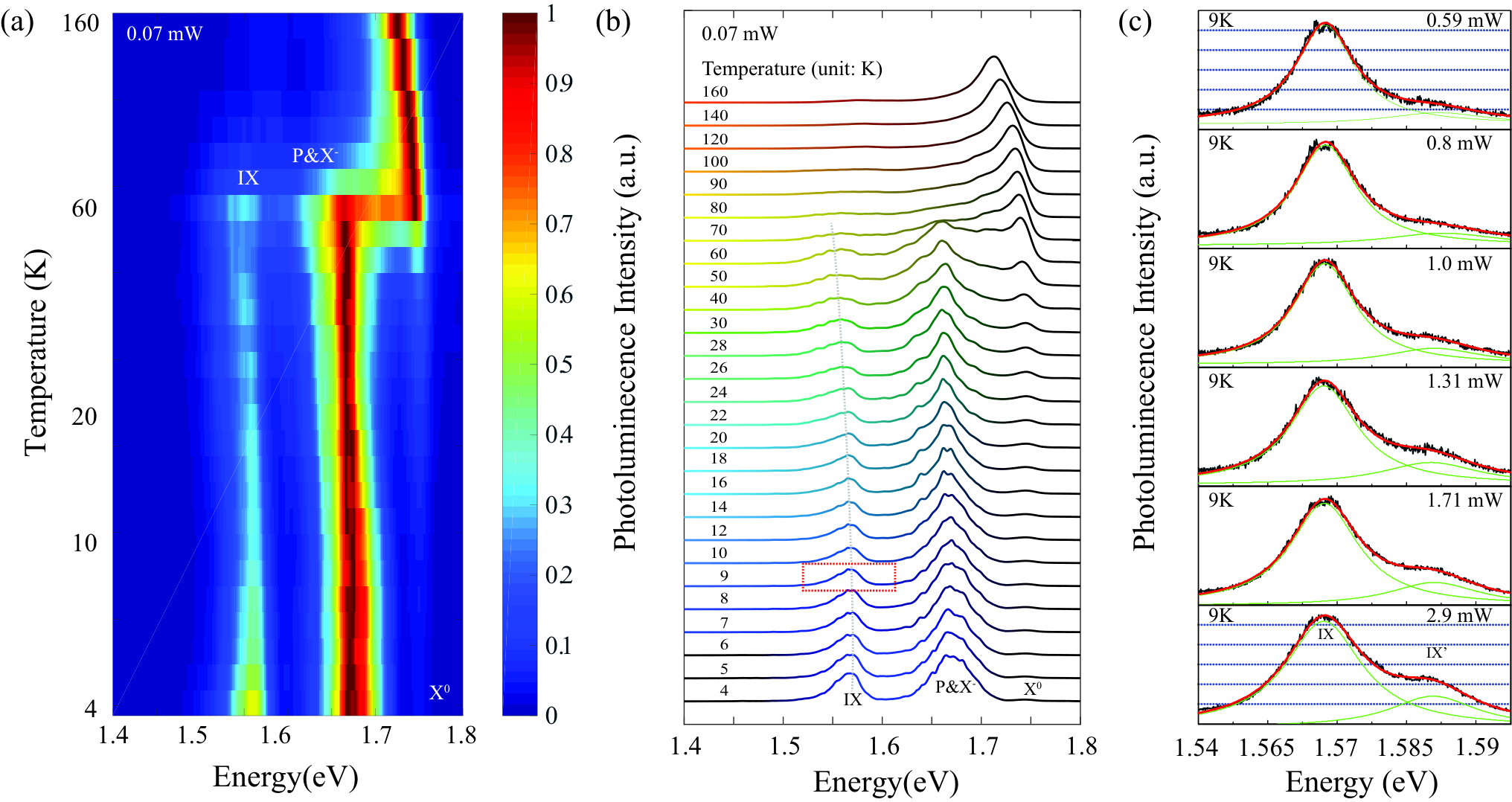


Figure 2 shows the results of the temperature-dependent PL for the same structure. The pronounced IX peaks become attenuated as the temperature increases and quench gradually up to 60 K. The dashed gray line in Fig. 2(b) follows the shift of the band gap as a function of the temperature. Fig. 2(c) shows the IX emission at 9 K as the power of a mode-locked Ti: sapphire pump laser ( eV) was varied. A bi-Lorentzian fit was applied to the data (black line), which was normalized by pump power and charge-coupled device (CCD) integration time. The higher energy and lower energy Lorentzians are shown with the two green lines. The relative intensity of these two sub-peaks changed as we increased the pump power. We define as the intensity of the higher-energy Lorentzian integrated over all energies, while corresponds to the lower energy Lorentzian. The ratio of these two integrated quantities, , was found to be and at pump powers of 0.59 mW and 2.9 mW respectively. The power dependence of this ratio implies that the IXs predominantly occupy the lower energy state at low power but begin to occupy the upper state at high power, which may be due to the laser heating the sample and giving a higher effective temperature. A power-dependent blueshift of the IXs has been reported by two other groups Rivera et al. 2015; Wang et al. 2018; however, it is not seen here because the hBN spacer layer significantly decreased the IX's density.
A further analysis was performed to measure the peak intensity of the intralayer and interlayer excitons as a function of the temperature. The result was fit with the thermal distribution function
| (1) |
Here Id and Iin are the peak intensity of direct (intralayer) and indirect (interlayer) excitons, respectively, and is the Boltzmann constant. We find that the temperature dependence has two distinct regimes, separated by a kink around 30 K, as seen in the plot of the relative intensity as a function of in Fig 3. Fitting the data with a line in regime I, which corresponds to temperatures above 30 K, gives meV. This is consistent with the splitting between the two lines, measured directly at 100 K as 193 meV. The same fitting procedure in regime II (below 30 K) gives meV, which is much lower than the measured energy splitting, around 182 meV at 9 K. This may indicate that the exciton states are no longer in thermal equilibrium, e.g., because excitons in the upper state cannot relax efficiently into the lower state, and/or it may indicate that dark (non-light-emitting) exciton states play a significant role in thermalization below 30 K. This is plausible as dark excitons have been observed at cryogenic temperatures Zhou et al. 2017, and the energy splitting of the dark and bright exciton in WSe2 has been estimated as 16 meVEcheverry et al. 2016.
Time-resolved PL measurements were performed using a Hamamatsu streak camera with a temporal resolution of 1 ps, mounted on an exit port of an 0.5-m spectrometer equipped with a 50 grooves/mm reflective grating. A mode-locked pulsed Ti: sapphire laser set to wavelength 711 nm ( eV) was used for pumping the heterostructures. A 750 nm long-pass filter was placed in the signal’s path to block the pump laser. Fig. 4(a) shows the wavelength-resolved streaked image, with calibrated time axis. The red dotted line is centered on the IX emission, around 790 nm. The time-resolved PL is plotted in Fig. 4(b) for T=7 K for two different pump powers, 0.59 mW and 2.9 mW. The time is defined as the point of maximum PL. The curvature of these plots at early times indicates that the decay process of the IXs is nontrivial. We expect that the decay rate equation for the IX density is governed by two terms,
| (2) |
where is the IX density, is the lifetime and is an Auger coefficient, corresponding to a nonradiative process in which two excitons collide, and one recombines, giving its energy to ionizing the other exciton, which then reappears when the hot electron and hole lose enough energy to bind to each other againSnoke and Kavoulakis 2014. The second term describes radiative recombination, which dominates at low density. The radiative lifetime for the IXs at 7 K under excitation power of 0.59 mW was found as ps, by linearly fitting the tail in Fig 4(b) at late times. The result is compared with fits of the whole time dependence using Equation (2) ( ps). The lifetime at a late time is not affected significantly by the Auger recombination, which means the Auger recombination dominates the initial decaying. Figure 4(c) shows the decay rate at intermediate times in the time range of 150 - 250 ps, after the initial thermalization of the carriers but while their density is still high, as a function of temperature, and Figure 4(d) shows the decay rate in the same time range, as a function of density. The increase of the decay rate with density is consistent with an Auger recombination mechanism, but may also be the result of the higher density leading to higher temperature. The decay process in sample 2 shows similar behavior (see supplementary information).
3 Summary
In this paper, we have shown that interlayer excitons can be observed in a vertical stacked structure of hBN/WSe2/hBN/p:WSe2/hBN, which is similar to a double quantum well. As expected, the energy position of the IX states is quite sensitive to the thickness of the spacer between the two layers.
The photoluminescence of the IXs is fit by a bi-Lorentzian, showing two IX states with different energies. The intensity ratio of the IXs and intralayer excitons follows the standard thermal distribution when the system is above 30 K. However, below 30 K there is a large discrepancy, leading us to believe that dark excitons play a significant role in low temperature thermalization.
The lifetime of the IXs is affected by the temperature and the excitation power. This indicates that not only direct excitons, but also indirect excitons, are subject to an Auger process, which the hBN spacer layer does not prevent.
Much earlier work has studied indirect excitons in GaAs/AlGaAs double quantum well structures, including very long transport distanceVörös et al. 2005. The current results indicate that many of these same results may be possible to reproduce in TMD-based heterostructures. The simplified sandwich structure of the multiple layers TMDs and the tunability of the IX energy either by modifying the thickness of the spacer or with the external electric field makes this structure appealling for embedding in an optical microcavity to create polariton statesLiu et al. 2014; Sun et al. 2017. It also may have implications for the search of IX condensation and new optoelectronics applications in 2D semiconductors.
The authors declare no competing interests.
- •
The Supporting Information is available free of charge online. The SI includes the schematic of the decay channels of the heterostructure; the Auger process analysis; temperature dependent spectra of the monolayer WSe2, p:WSe2, and a control sample with the same configuration as the one shows in the manuscript but possesses a different thickness of the spacer.
References
- Butov et al. (2002) Butov, L. V.; Lai, C. W.; Ivanov, A. L.; Gossard, A. C.; Chemla, D. S. Towards Bose-Einstein condensation of excitons in potential traps. Nature 2002, 417, 47–52.
- Vörös et al. (2006) Vörös, Z.; Snoke, D. W.; Pfeiffer, L.; West, K. Trapping Excitons in a Two-Dimensional In-Plane Harmonic Potential: Experimental Evidence for Equilibration of Indirect Excitons. Phys. Rev. Lett. 2006, 97, 016803.
- Ross et al. (2014) Ross, J. S.; Klement, P.; Jones, A. M.; Ghimire, N. J.; Yan, J.; Mandrus, D. G.; Taniguchi, T.; Watanabe, K.; Kitamura, K.; Yao, W.; Cobden, D. H.; Xu, X. Electrically tunable excitonic light-emitting diodes based on monolayer WSe2 p-n junctions. Nature Nanotechnology 2014, 9, 268–272.
- Koperski et al. (2015) Koperski, M.; Nogajewski, K.; Arora, A.; Cherkez, V.; Mallet, P.; Veuillen, J. Y.; Marcus, J.; Kossacki, P.; Potemski, M. Single photon emitters in exfoliated WSe2 structures. Nature Nanotechnology 2015, 10, 503–506.
- Schaibley et al. (2016) Schaibley, J. R.; Yu, H.; Clark, G.; Rivera, P.; Ross, J. S.; Seyler, K. L.; Yao, W.; Xu, X. Valleytronics in 2D materials. Nature Reviews Materials 2016, 1, 16055.
- Xu et al. (2014) Xu, X.; Yao, W.; Xiao, D.; Heinz, T. F. Spin and pseudospins in layered transition metal dichalcogenides. Nature Physics 2014, 10, 343–350.
- Lopez-Sanchez et al. (2013) Lopez-Sanchez, O.; Lembke, D.; Kayci, M.; Radenovic, A.; Kis, A. Ultrasensitive photodetectors based on monolayer MoS 2. Nature Nanotechnology 2013, 8, 497–501.
- Chernikov et al. (2014) Chernikov, A.; Berkelbach, T. C.; Hill, H. M.; Rigosi, A.; Li, Y.; Aslan, O. B.; Reichman, D. R.; Hybertsen, M. S.; Heinz, T. F. Exciton Binding Energy and Nonhydrogenic Rydberg Series in Monolayer . Phys. Rev. Lett. 2014, 113, 076802.
- Ugeda et al. (2014) Ugeda, M. M.; Bradley, A. J.; Shi, S. F.; Da Jornada, F. H.; Zhang, Y.; Qiu, D. Y.; Ruan, W.; Mo, S. K.; Hussain, Z.; Shen, Z. X.; Wang, F.; Louie, S. G.; Crommie, M. F. Giant bandgap renormalization and excitonic effects in a monolayer transition metal dichalcogenide semiconductor. Nature Materials 2014, 13, 1091–1095.
- Liu et al. (2014) Liu, X.; Galfsky, T.; Sun, Z.; Xia, F.; Lin, E. C.; Lee, Y. H.; Kéna-Cohen, S.; Menon, V. M. Strong light-matter coupling in two-dimensional atomic crystals. Nature Photonics 2014, 9, 30–34.
- Sun et al. (2017) Sun, Z.; Gu, J.; Ghazaryan, A.; Shotan, Z.; Considine, C.; Dollar, M.; Chakraborty, B.; Liu, X.; Ghaemi, P.; Kéna-Cohen, S.; Menon, V. Optical control of roomerature valley polaritons. Nature Photonics 2017, 11, 491–496.
- Chakraborty et al. (2018) Chakraborty, B.; Gu, J.; Sun, Z.; Khatoniar, M.; Bushati, R.; Boehmke, A. L.; Koots, R.; Menon, V. M. Control of Strong Light-Matter Interaction in Monolayer WS2 through Electric Field Gating. Nano Letters 2018, 18, 6455–6460.
- Zhou et al. (2020) Zhou, H.; Zhao, Y.; Tao, W.; Li, Y.; Zhou, Q.; Zhu, H. Controlling Exciton and Valley Dynamics in Two-Dimensional Heterostructures with Atomically Precise Interlayer Proximity. ACS Nano 2020, 14, 4618–4625.
- Rivera et al. (2015) Rivera, P.; Schaibley, J. R.; Jones, A. M.; Ross, J. S.; Wu, S.; Aivazian, G.; Klement, P.; Seyler, K.; Clark, G.; Ghimire, N. J.; Yan, J.; Mandrus, D. G.; Yao, W.; Xu, X. Observation of long-lived interlayer excitons in monolayer MoSe 2-WSe 2 heterostructures. Nature Communications 2015, 6, 4–9.
- Hong et al. (2014) Hong, X.; Kim, J.; Shi, S. F.; Zhang, Y.; Jin, C.; Sun, Y.; Tongay, S.; Wu, J.; Zhang, Y.; Wang, F. Ultrafast charge transfer in atomically thin MoS2/WS2 heterostructures. Nature Nanotechnology 2014, 9, 682–686.
- Rivera et al. (2016) Rivera, P.; Seyler, K. L.; Yu, H.; Schaibley, J. R.; Yan, J.; Mandrus, D. G.; Yao, W.; Xu, X. Valley-polarized exciton dynamics in a 2D semiconductor heterostructure. Science 2016, 351, 688–691.
- Lee et al. (2014) Lee, C. H.; Lee, G. H.; Van Der Zande, A. M.; Chen, W.; Li, Y.; Han, M.; Cui, X.; Arefe, G.; Nuckolls, C.; Heinz, T. F.; Guo, J.; Hone, J.; Kim, P. Atomically thin p-n junctions with van der Waals heterointerfaces. Nature Nanotechnology 2014, 9, 676–681.
- Karni et al. (2019) Karni, O.; Barré, E.; Lau, S. C.; Gillen, R.; Ma, E. Y.; Kim, B.; Watanabe, K.; Taniguchi, T.; Maultzsch, J.; Barmak, K.; Page, R. H.; Heinz, T. F. Infrared Interlayer Exciton Emission in Heterostructures. Phys. Rev. Lett. 2019, 123, 247402.
- Unuchek et al. (2019) Unuchek, D.; Ciarrocchi, A.; Avsar, A.; Sun, Z.; Watanabe, K.; Taniguchi, T.; Kis, A. Valley-polarized exciton currents in a van der Waals heterostructure. Nature Nanotechnology 2019, 14, 1104–1109.
- Wang et al. (2018) Wang, Z.; Chiu, Y. H.; Honz, K.; Mak, K. F.; Shan, J. Electrical Tuning of Interlayer Exciton Gases in WSe2 Bilayers. Nano Letters 2018, 18, 137–143.
- Fang et al. (2014) Fang, H. et al. Strong interlayer coupling in van der Waals heterostructures built from single-layer chalcogenides. Proceedings of the National Academy of Sciences 2014, 111, 6198–6202.
- Calman et al. (2018) Calman, E. V.; Fogler, M. M.; Butov, L. V.; Hu, S.; Mishchenko, A.; Geim, A. K. Indirect excitons in van der Waals heterostructures at room temperature. Nature Communications 2018, 9, 1–5.
- Latini et al. (2017) Latini, S.; Winther, K. T.; Olsen, T.; Thygesen, K. S. Interlayer Excitons and Band Alignment in MoS2/hBN/WSe2 van der Waals Heterostructures. Nano Letters 2017, 17, 938–945.
- Sun et al. (2014) Sun, D.; Rao, Y.; Reider, G. A.; Chen, G.; You, Y.; Brézin, L.; Harutyunyan, A. R.; Heinz, T. F. Observation of rapid exciton-exciton annihilation in monolayer molybdenum disulfide. Nano Letters 2014, 14, 5625–5629.
- Taniguchi and Watanabe (2007) Taniguchi, T.; Watanabe, K. Synthesis of high-purity boron nitride single crystals under high pressure by using Ba–BN solvent. Journal of Crystal Growth 2007, 303, 525 – 529.
- Yan et al. (2014) Yan, T.; Qiao, X.; Liu, X.; Tan, P.; Zhang, X. Photoluminescence properties and exciton dynamics in monolayer WSe 2 . Applied Physics Letters 2014, 105, 101901.
- Liu et al. (2013) Liu, G. B.; Shan, W. Y.; Yao, Y.; Yao, W.; Xiao, D. Three-band tight-binding model for monolayers of group-VIB transition metal dichalcogenides. Physical Review B 2013, 88, 085433.
- Komider et al. (2013) Komider, K.; González, J. W.; Fernández-Rossier, J. Large spin splitting in the conduction band of transition metal dichalcogenide monolayers. Physical Review B 2013, 88, 245436.
- Kormányos et al. (2015) Kormányos, A.; Burkard, G.; Gmitra, M.; Fabian, J.; Zólyomi, V.; Drummond, N. D.; Fal, V. Erratum: K·p theory for two-dimensional transition metal dichalcogenide semiconductors. 2D Materials 2015, 2, 22001.
- Zhou et al. (2017) Zhou, Y.; Scuri, G.; Wild, D. S.; High, A. A.; Dibos, A.; Jauregui, L. A.; Shu, C.; De Greve, K.; Pistunova, K.; Joe, A. Y.; Taniguchi, T.; Watanabe, K.; Kim, P.; Lukin, M. D.; Park, H. Probing dark excitons in atomically thin semiconductors via near-field coupling to surface plasmon polaritons. Nature Nanotechnology 2017, 12, 856–860.
- Echeverry et al. (2016) Echeverry, J. P.; Urbaszek, B.; Amand, T.; Marie, X.; Gerber, I. C. Splitting between bright and dark excitons in transition metal dichalcogenide monolayers. Phys. Rev. B 2016, 93, 121107.
- Snoke and Kavoulakis (2014) Snoke, D.; Kavoulakis, G. M. Bose–Einstein condensation of excitons in Cu2O: progress over 30 years. Reports on Progress in Physics 2014, 77, 116501.
- Vörös et al. (2005) Vörös, Z.; Balili, R.; Snoke, D. W.; Pfeiffer, L.; West, K. Long-Distance Diffusion of Excitons in Double Quantum Well Structures. Phys. Rev. Lett. 2005, 94, 226401.
TOC Graphic
![[Uncaptioned image]](2001.01009v7/TOC.png)