Flexible Communication Avoiding Matrix Multiplication
on FPGA with
High-Level Synthesis
Abstract.
Data movement is the dominating factor affecting performance and energy in modern computing systems. Consequently, many algorithms have been developed to minimize the number of I/O operations for common computing patterns. Matrix multiplication is no exception, and lower bounds have been proven and implemented both for shared and distributed memory systems. Reconfigurable hardware platforms are a lucrative target for I/O minimizing algorithms, as they offer full control of memory accesses to the programmer. While bounds developed in the context of fixed architectures still apply to these platforms, the spatially distributed nature of their computational and memory resources requires a decentralized approach to optimize algorithms for maximum hardware utilization. We present a model to optimize matrix multiplication for FPGA platforms, simultaneously targeting maximum performance and minimum off-chip data movement, within constraints set by the hardware. We map the model to a concrete architecture using a high-level synthesis tool, maintaining a high level of abstraction, allowing us to support arbitrary data types, and enables maintainability and portability across FPGA devices. Kernels generated from our architecture are shown to offer competitive performance in practice, scaling with both compute and memory resources. We offer our design as an open source project11 1 https://github.com/spcl/gemm_hls (10.5281/zenodo.3559536) to encourage the open development of linear algebra and I/O minimizing algorithms on reconfigurable hardware platforms.

1. Introduction
The increasing technological gap between computation and memory speeds (Wulf and McKee 1995) pushes both academia (Solomonik and Demmel 2011; Scquizzato and Silvestri 2013; Demmel et al. 2013; Aggarwal and Vitter 1988) and industry (Intel 2007; Anderson et al. 1999) to develop algorithms and techniques to minimize data movement. The first works proving I/O lower bounds for specific algorithms, e.g., Matrix Matrix Multiplication (MMM), date back to the 80s (Jia-Wei and Kung 1981). The results were later extended to parallel and distributed machines (Irony et al. 2004b). Since then, many I/O minimizing algorithms were developed for linear algebra (Solomonik and Demmel 2011; Geist and Ng 1990; Anderson et al. 2011), neural networks (Demmel and Dinh 2018), and general programs that access arrays (Christ et al. 2013). Minimizing I/O impacts not only performance, but also reduces bandwidth usage in a shared system. MMM is typically used as a component of larger applications (Vanhoucke et al. 2011; Del Ben et al. 2015), where it co-exists with other algorithms, e.g., memory bound linear algebra operations such as matrix-vector/vector-vector operations, which benefit from a larger share of the bandwidth, but do not require large amounts of compute resources.
FPGAs are an excellent platform for accurately modeling performance and I/O to guide algorithm implementations. In contrast to software implementations, the replacement of cache with explicit on-chip memory, and isolation of the instantiated architecture, yields fully deterministic behavior in the circuit: accessing memory, both on-chip and off-chip, is always done explicitly, rather than by a cache replacement scheme fixed by the hardware. The models established so far, however, pose a challenge for their applicability on FPGAs. They often rely on abstracting away many hardware details, assuming several idealized processing units with local memory and all-to-all communication (Solomonik and Demmel 2011; Aggarwal and Vitter 1988; Jia-Wei and Kung 1981; Irony et al. 2004b). Those assumptions do not hold for FPGAs, where the physical area size of custom-designed processing elements (PEs) and their layout are among most important concerns in designing efficient FPGA implementations (Lavin and Kaviani 2018). Therefore, performance modeling for reconfigurable architectures requires taking constraints like logic resources, fan-out, routing, and on-chip memory characteristics into account.
With an ever-increasing diversity in available hardware platforms, and as low-precision arithmetic and exotic data types are becoming key in modern DNN (Ben-Nun and Hoefler 2019) and linear solver (Haidar et al. 2018) applications, extensibility and flexibility of hardware architectures will be crucial to stay competitive. Existing high-performance FPGA implementations (Moss et al. 2018; Jovanović and Milutinovic 2012) are implemented in hardware description languages (HDLs), which drastically constrains their maintenance, reuse, generalizability, and portability. Furthermore, the source code is not disclosed, such that third-party users cannot benefit from the kernel or build on the architecture.
In this work, we address all the above issues. We present a high-performance, communication avoiding MMM algorithm, which is based on both computational complexity theory (Jia-Wei and Kung 1981) (Section 3.2), and on detailed knowledge of FPGA-specific features (Section 4). Our architecture is implemented in pure C++ with a small and readable code base, and to the best of our knowledge, is the first open source, high-performance MMM FPGA code. We do not assume the target hardware, and allow easy configuration of platform, degree of parallelism, buffering, data types, and matrix sizes, allowing kernels to be specialized to the desired scenario. The contributions of this paper are:
- •
We model a decomposition for matrix multiplication that simultaneously targets maximum performance and minimum off-chip data movement, in terms of hardware constants.
- •
We design a mapping that allows the proposed scheme to be implemented in hardware, using the model parameters to lay out the architecture.
- •
We provide a plug-and-play, open source implementation of the hardware architecture in pure HLS C++, enabling portability across FPGA and demonstrating low code complexity.
- •
We include benchmarks for a wide range of floating point and integer types, and show the effect of adjusting parallelism and buffer space in the design, demonstrating the design’s flexibility and scalability.
2. Optimization Goals
In this section we introduce what we optimize. In Sections 3.2, 3.3, and 4 we describe how this is achieved. We consider optimizing the schedule of a classical MMM algorithm, that is, given a problem of finding , where , an algorithm performs multiplications and additions (pseudocode shown in Lst. 3). We therefore exclude Strassen-like routines (Strassen 1969) from our analysis, as the classical algorithms often perform better on practical problems and hardware (D’Alberto and Nicolau 2008). We require that the optimal schedule: (1) achieves highest performance (takes least time-to-solution time), while (2) performing the least number of I/O operations, by (3) making most efficient use of resources.
Computation
On general purpose CPUs, as well as on modern GPUs, optimizing for computation is often a straightforward task. Exploiting techniques like vectorization or data alignment (Zhou and Xue 2016) can mostly be offloaded to compilers. Thus, most of the effort is spent on I/O minimization. When targeting FPGAs, designing an architecture that can optimally exploit available logic, even for computationally simple algorithms such as matrix multiplication, requires significant engineering effort. We must thus maintain a decomposition that is efficiently implementable in hardware, while achieving the desired theoretical properties.
I/O
Schedule optimization on a parallel machine determines both the domain decomposition (which computations are assigned to which compute units), and sequential execution (the order in which each compute unit executes its tasks). The former impacts communication between compute units (a.k.a. horizontal I/O), and the latter is responsible for the communication between a compute unit and a main memory (a.k.a. a vertical I/O). Both aspects of the parallel schedule are constrained by available resources and their interdependencies (e.g., NUMA domains or limited fan-out on FPGAs).
Resources
When targeting a high utilization design on FPGA, it is critical to maintain characteristics that aid the routing process. Routing reacts poorly to large fan-in or fan-out, which typically occurs when these are dependent on the degree of parallelism: that is, if determines the degree of parallelism in the program, -to- and -to- connections in the architecture should be avoided. This is true both on the granularity of individual logic units, and on the granularity of coarse-grained modules instantiated by the programmer. To accommodate this, we can regulate the size of PEs, and favor PE topologies that are easily mapped to a plane, such as grids or chains. Furthermore, mapping of a hardware architecture to the chip logic and interconnect (placement and routing) may reduce the clock frequency due to long routing paths. Due to the intractable size of the configuration space, this cannot be efficiently modeled and requires empirical evaluation of designs. The routing challenges are exasperated in FPGA chips that consist of multiple “chiplets”, such as the Xilinx UltraScale+ VU9P chip used in this paper, which hosts three “super-logical regions” (SLRs). Crossing the chiplets consumes highly limited routing resources and carries a higher timing penalty. Limiting these crossings is thus key to scaling up resource utilization.
| MMM | , , | Unit vectors spanning 3D iteration space. |
| , , | Matrix sizes in , , and dimensions, respectively. | |
| , | Input matrices and . | |
| Output matrix . | ||
| naming | Parameter naming convention. is some quantity | |
| (i.e., size or number of objects), is an object that | ||
| refers to. | ||
| Hardware limit on a parameter . | ||
| The product of all tile sizes. | ||
| Total number of objects. | ||
| Number of objects in (or ) dimension in the | ||
| enveloping tile. | ||
| Intrinsic size of an object. | ||
| Bit width of object (e.g., of port or data type). | ||
| Vector of logic resources. | ||
| Compute units in a processing element. | ||
| Processing elements in a compute tile. | ||
| Compute tiles in a block tile. | ||
| Block tiles in a memory tile. | ||
| optimization | Total size of available on-chip memory. | |
| Total number of compute units. | ||
| Total number of off-chip memory transfers. | ||
| Total number of multiply-addition operations | ||
| required to perform MMM. | ||
| Achieved and maximum design frequency. | ||
| Design total execution time. |
Throughout this paper, we use the two-level notation for naming parameters (Table 1). Most of the parameter names are in the form of , where refers to some quantity, such as the total number of objects, and determines what is the object of interest. E.g., , are: total number of () compute units (), memory blocks (), and a size of each memory block (), respectively.
The target hardware contains types of different logic resources. This typically consists of general purpose logic, such as lookup tables (LUTs), and more specialized arithmetic units, such as digital signal processing units (DSPs). We represent a quantity of these resources as a vector . As a basic logical entity, we consider a “compute unit”, which is a basic circuit able to perform a single multiply-addition operation in a single cycle. Each unit is implemented on the target hardware using some combination of logic resources . Depending on the numerical precision, different number of computation resources are needed to form a single compute unit, so the maximum number of compute units that can be instantiated, , may vary. The compute units are organized into processing elements (PEs), which encapsulate a closed logical task (e.g., a vector operation) of compute units. Each PE additionally consumes logic resources as orchestration overhead. This gives us the following constraint, which enforces that the total amount of resources consumed by compute units and their encompassing PEs should not exceed the total resources available:
| (1) | ||||
where is the dimensionality of the resource vector (illustrated in the top-right side of Fig. 2).
3. Optimization Models
3.1. Computation Model
To optimize computational performance we minimize the total execution runtime, which is a function of achieved parallelism (total number of compute units ) and the design clock frequency . The computational logic is organized into PEs, and we assume that every PE holds compute units in dimensions and (see Tab. 1 for an overview of all symbols used). We model the factor directly in the design, and rely on empirically fixing , which is limited by the maximum size of data buses between PEs (i.e., and , where depends on the architecture, and typically takes values up to ). Formally, we can write the computational optimization problem as follows:
| (2) | ||||
That is, the time to completion is minimized when is maximized, where the number of parallel compute units is constrained by the available logic resources of the design (this can be the full hardware chip, or any desired subset resource budget). We respect routing constraints by observing a maximum bus width , and must stay within the target frequency .
3.2. I/O Model
3.2.1. State-of-the-art of Modeling I/O for MMM
Minimizing the I/O cost is essential for achieving high performance on modern architectures, even for traditionally compute-bound kernels like MMM (Kwasniewski et al. 2019). In this section, we sketch a theoretical background from previous works which lays foundation for our FPGA model. Following the state-of-the-art I/O models (Jia-Wei and Kung 1981; Irony et al. 2004a; Solomonik and Demmel 2011) we assume that a parallel machine consists of processors, each equipped with a fast private memory of size words. To perform an arithmetic operation, processor is required to have all operands in its fast memory. The principal idea behind the I/O optimal schedule is to maximize the computational intensity, i.e., the number of arithmetic operations performed per one I/O operation. This naturally expresses the notion of data reuse, which reduces both vertical (through memory hierarchy) and horizontal (between compute units) I/O (Section 2).
Algorithm as a Graph
We represent an entire execution of an algorithm as a computation directed acyclic graph (CDAG) (Chaitin et al. 1981; Jia-Wei and Kung 1981; Kwasniewski et al. 2019) , where every vertex corresponds to some unique value during the execution, and edges represent data dependencies between them. Vertices without incoming edges are inputs, and the ones without outgoing edges are outputs. The remaining vertices are intermediate results. In the context of MMM, matrices and form and input vertices, respectively, and partial sums of form intermediate vertices, with inputs both from corresponding vertices of and , and previous partial sums of . The output vertices are formed by the vertices of which represent the last of partial sums. The MMM CDAG is shown in Fig. 1a.
I/O as Graph Pebbling
Hong and Kung (Jia-Wei and Kung 1981) introduced the red-blue pebble game abstraction to model the I/O cost of a sequential schedule on a CDAG. We refer a reader to the original paper for the formal definition and details of this game: here we just draw its simplistic sketch. The key idea is to play a pebbling game with a limited number of red pebbles (corresponding to the small-but-fast memory) and an unlimited number of blue pebbles (large, slow memory). The rules are that one can put a red pebble on a vertex only if all its direct predecessors also have red pebbles (which represent computing a value, while all operands are in the fast memory). Placing a blue pebble on a red one corresponds to a store operation, and putting a red pebble on a blue corresponds to a load. Initially, only input vertices have blue pebbles on them. The goal is to put blue pebbles on the output vertices. In this model, the I/O optimal schedule is a sequence of pebbling moves which minimizes the load and store operations.
Schedule as a Graph Partition
In our work, we extend the methodology and results of COSMA (Kwasniewski et al. 2019), which is based on the red-blue pebble game. We partition the CDAG into disjoint subsets (a.k.a. subcomputations) , such that each has a constant number of input and output vertices (which form the Dominator set and Minimum set, respectively). The collection of all is called an -partition of . The authors show that an I/O optimal scheme can be derived from finding an -partition of a smallest cardinality, for some value of . We will use this result to build our model.
Optimal Graph Partition as Maximizing Computational Intensity
In COSMA (Kwasniewski et al. 2019), it is shown that the I/O optimal MMM schedule maximizes the computational intensity of each subcomputation , that is, the number of arithmetic operations per I/O operation. Formally:
| (3) | ||||
where is a number of values updated in subcomputation , is the number of inputs of (the Dominator set), is the number of inputs that are already in the on-chip memory (data reuse), and is the number of partial results that have to be stored back to off-chip memory. Therefore, we aim to maximize utilization of all available on-chip memory, to increase the reuse of data that is already loaded. The sets , , and are depicted in Fig. 1b.
3.2.2. Extending to the FPGA Scenario
I/O Optimal Schedule vs. FPGA Constraints
State-of-the-art I/O models (Jia-Wei and Kung 1981; Irony et al. 2004a; Solomonik and Demmel 2011) assume that a parallel machine consists of processors, each equipped with a small private memory of constant size words (two-level memory model). Under these assumptions, COSMA establishes that the I/O optimal MMM schedule is composed of subcomputations, each performing multiply-addition operations while loading elements from matrices and . However, in the FPGA setting these assumptions do not hold, as the number of compute units is a variable depending on both hardware resources (which is constant), and on the processing element design. Furthermore, the mapping between processing elements and available BRAM blocks is also constrained by ports and limited fan-out. We impose the additional requirement that compute and memory resources must be equally distributed among PEs, posing additional restrictions on a number of available resources and their distribution for each subcomputation to secure maximum arithmetic throughput and routing feasibility:
- (1)
The number of parallel compute units is maximized.
- (2)
The work is load balanced, such that each compute unit performs the same number of computations.
- (3)
Each memory block is routed to only one compute unit (i.e., they are not shared between compute units).
- (4)
Each processing element performs the same logical task, and consumes the same amount of computational and memory block resources.
Memory resources
To model the memory resources of the FPGA, we consider the bit-length of , depending on the target precision. The machine contains on-chip memory blocks, each capable of holding words of the target data type, yielding a maximum of
words that can be held in on-chip memory. takes different values depending on (e.g., for half precision floating point, or a long unsigned integer). Each memory block supports one read and one write of up to bits in a single cycle in a pipelined fashion.
FPGA-constrained I/O Minimization
We denote each as a memory tile , as its size in and dimensions determines the memory reuse. To support a hierarchical hardware design, each is further decomposed into several levels of tiling. This decomposition encapsulates hardware features of the chip, and imposes several restrictions on the final shape of . The tiling scheme is illustrated in Fig. 2. We will cover the purpose and definition of each layer in the hierarchy shortly in Sec. 3.3, but for now use that the dimensions of the full memory tile are:
| (4) | ||||
and we set . Following the result from (Kwasniewski et al. 2019), a schedule that minimizes the number I/O operations, loads elements of one column of matrix , elements of one row of matrix and reuses previous partial results of , thus computing an outer product of the loaded row and column. We now rewrite Eq. 3 as:
| (5) | ||||
and the total number of I/O operations as:
| (6) |
This expression is minimized when:
| (7) |
That is, a memory tile is a square of size . Eq. 6 therefore gives us a theoretical lower bound on , assuming that all available memory can be used effectively. However, the assumptions stated in Sec. 3.2 constrain the perfect distribution of hardware resources, which we model in Sec. 3.3.
3.3. Resource Model
Based on the I/O model and the FPGA constraints, we create a logical hierarchy which encapsulates various hardware resources, which will guide the implementation to maximize I/O and performance. We assume a chip contains different hardware resources (see Sec. 1). The dimensionality and length of a vector depends on the target hardware – e.g., Intel Arria 10 and Stratix 10 devices expose native floating point DSPs, each implementing a single operation, whereas a Xilinx UltraScale+ device requires a combination of logic resources. We model fast memory resources separately as memory blocks (e.g., M20K blocks on Intel Stratix 10, or Xilinx BRAM units). We consider a chip contains memory blocks, where each unit can store elements of the target data type and has a read/write port width of bits. The scheme is organized as follows (shown in Fig. 2):
- (1)
A compute unit consumes hardware resources, and can throughput a single multiplication and addition per cycle. Their maximal number
for a given numerical precision is a hardware constant, given by the available resources .
- (2)
A processing element encapsulates compute units. Each processing element requires additional resources for overhead logic.
- (3)
A compute tile encapsulates processing elements. One compute tile contains all available compute units
. - (4)
A block tile encapsulates compute tiles, filling the entire internal capacity of currently allocated memory blocks.
- (5)
A memory tile encapsulates block tiles (discussed below), using all available memory blocks.
Pseudocode showing the iteration space of this decomposition is shown in
Lst. 4, consisting of 11 nested loops. Each loop is either a
sequential for-loop, meaning that no iterations will overlap,
and will thus correspond to pipelined loops in the HLS code; or a
parallel forall-loop, meaning that every iteration is executed
every cycle, corresponding to unrolled loops in the HLS code. We require
that the sequential loops are coalesced into a single pipeline, such that no
overhead is paid at iterations of the outer loops.
3.4. Parallelism and Memory Resources
The available degree of parallelism, counted as a number of simultaneous computations of line 17 in Listing 4, is determined by the number of compute units . Every one of these compute units must read and write an element of from fast memory every cycle. This implies a minimum number of parallel fast memory accesses that must be supported in the architecture. Memory blocks expose a limited access width (measured in bits), which constrains how much data can be read from/written to them in a single cycle. We can thus infer a minimum number of memory blocks necessary to serve all compute units in parallel, given by:
| (8) |
where is the width of the data type in bits, and denotes the granularity of a processing element. Because all accesses within a processing element happen in parallel, accesses to fast memory can be coalesced into long words of size bits. For cases where is not a multiple of , the ceiling in Eq. 8 may be significant for the resulting . When instantiating fast memory to implement the tiling strategy, Eq. 8 defines the minimum “step size” we can take when increasing the tile sizes.
Within a full memory tile, each updated value is reused after all elements in a single memory tile are evaluated, and computation proceeds to the next iteration of the -loop (line 4 in Listing 4). Given the intrinsic size of each memory block , we can thus perform iterations of the compute tile before a single batch of allocated memory blocks has been filled up. If the total number of memory blocks , i.e., the number of blocks required to support the parallel access requirements is less than the total number of blocks available, we can perform additional iterations of the block tile, using all available memory blocks (up to the additive factor of ). However, for large available parallelism , this additive factor may play a significant role, resulting in a part of available on-chip memory not being used. This effect is depicted in Fig. 5 for different values of for the case of single precision floating point (FP32) in Xilinx BRAM blocks, where and . The total number of memory blocks that can be efficiently used, without sacrificing the compute performance and load balancing constraints, is then:
| (9) |
In the worst case, this implies that only memory blocks are used. In the best case, is a multiple of , and all memory block resources can be utilized. When , the memory tile collapses to a single block tile, and the total memory block usage is equal to Eq. 8.
4. Hardware Mapping
With the goals for compute performance and I/O optimality set by the model, we now describe a mapping to a concrete hardware implementation.
4.1. Layout of Processing Elements
For Eq. 2 to hold, all PEs must run at full throughout execution of the kernel, computing distinct contributions to the output tile. In terms of the proposed tiling scheme, we must evaluate a full compute tile (second layer in Fig. 2) every cycle, which consists of PE tiles (first layer in Fig. 2), each performing calculations in parallel, contributing a total of multiplications and additions towards the outer product currently being computed. Assuming that elements of and a full row of elements of have been prefetched, we must – for each of the rows of the first layer in Fig. 2 – propagate values to all horizontal PEs, and equivalently for columns of . If this was broadcasted directly, it would lead to a total fan-out of for both inputs.
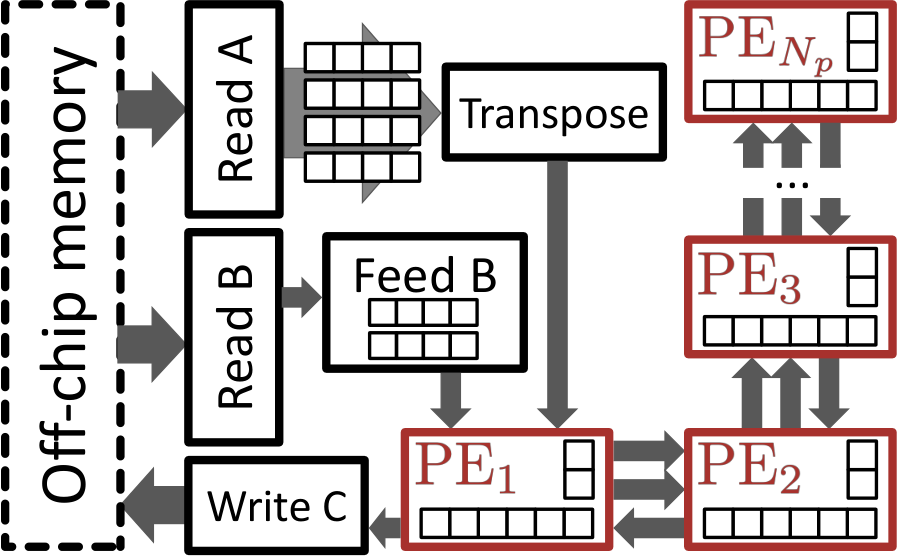
Rather than broadcasting, we can exploit the regular grid structure, letting each column forward values of , and each row forward values of , in a pipelined fashion. Such an architecture is sometimes referred to as a systolic array, and is illustrated in Fig. 6. In this setup, each processing element has three inputs and three outputs (for , , and ), and dedicated Feed A and Feed B modules send prefetched contributions to the outer product at the left and top edges of the grid, while Store C consumes the output values of written back by the PEs. The number of inter-module connections for this design is , but more importantly, the fan-out of all modules is now constant, with data buses per PE. Each PE is responsible for fully evaluating elements of the output tile of . The elements of each PE tile in Fig. 2 are stored contiguously (the first layer), but all subsequent layers are not – only the compute tile as a whole in contiguous in . Final results must thus be written back in an interleaved manner to achieve contiguous writes back to .
Collapsing to a 1D array.
Although the 2D array of PEs is intuitive for performing matrix multiplication, it requires a grid-like structure to be routed on the chip. While this solves the issue of individual fan-out – and may indeed be sufficient for monolithic devices with all logic arranged in a rectangular structure – we wish to map efficiently onto general interconnects, including non-uniform and hierarchical structures, as well as multiple-chiplet FPGAs (or, potentially, multiple FPGAs). To achieve this, we can optionally collapse the 2D array of PEs into a 1D array by fixing , resulting in PEs connected in sequence. Since this results in a long, narrow compute tile, we additionally fix , relying on to regulate the PE granularity. Forming narrow compute tiles is possible without violating Eq. 7, as long as and are kept identical (or as similar as possible), which we can achieve by regulating the outer block and tiling layers (the memory and block tile layers in Fig. 2).

Double buffering.
Since each PE in the 1D array now computes one or more full rows of the compute tile, we can buffer values of in internal registers, rather than from external modules. These can be propagated through the array from the first element to the last, then kept in local registers and applied to values of that are streamed through the array from a buffer before the first PE. Since the number of PEs in the final design is large, we overlap the propagation of new values of with the computation of the outer product contribution using the previous values of , by using double buffering, requiring two registers per PE, i.e., total registers across the design.
By absorbing the buffering of into the PEs, we have reduced the architecture to a simple chain of width , reducing the total number of inter-module connections for the compute to , with 3 buses connecting each PE transition. When crossing interconnects with long timing delays or limited width, such as connections between chiplets, this means that only 3 buses must cross the gap, instead of a number proportional to the circumference of the number of compute units within a single chiplet, as was the case for the 2D design. As a situational downside, this increases the number of pipeline stages in the architecture when maximizing compute, which means that the number of compute tiles must be larger than the number of PEs, i.e., . This extra constraint is easily met when minimizing I/O, as the block tile size is set to a multiple of (see Sec. 3.3), which in practice is higher than the number of PEs, assuming that extreme cases like are avoided for large .
4.2. Handling Loop-carried Dependencies
Floating point accumulation is often not a native operation on FPGAs, which can introduce loop-carried dependencies on the accumulation variable. This issue is circumvented with our decomposition. Each outer product consists of inner memory tiles. Because each tile reduces into a distinct location in fast memory, collisions are separated by cycles, and thus do not obstruct pipelining for practical memory tile sizes (i.e., where is bigger than the accumulation latency).
For data types such as integers or fixed point numbers, or architectures that support (and benefit from) pipelined accumulation of floating point types, it is possible to make the innermost loop, optionally tiling and further to improve efficiency of reads from off-chip memory. The hardware architecture for such a setup is largely the same as the architecture proposed here, but changes the memory access pattern.
4.3. Optimizing Column-wise Reads
In the outer product formulation, the -matrix must be read in a column-wise fashion. For memory stored as row-major, this results in slow and wasteful reads from DDR memory (in a column-major setting, the same argument applies, but for instead). For DDR4 memory, a minimum of 512 bits must be transferred to make up for the I/O clock multiplier, and much longer bursts are required to saturate DDR bandwidth in practice. To make up for this, we can perform on-the-fly transposition of as part of the hardware design in an additional module, by reading wide vectors and pushing them to separate FIFOs of depth , which are popped in transposed order when sent to the kernel (this module can be omitted in the implementation at configuration time if is pre-transposed, or an additional such module is added if is passed in transposed form).
4.4. Writing Back Results
Each final tile of is stored across the chain of processing in a way that requires interleaving of results from different PEs when writing it back to memory. Values are propagated backwards through the PEs, and are written back to memory at the head of the chain, ensuring that only the first PE must be close to the memory modules accessing off-chip memory. In previous work, double buffering is often employed for draining results, at the significant cost of reducing the available fast memory from to in Eq. 6, resulting in a reduction in the arithmetic intensity of . To achieve optimal fast memory usage, we can leave writing out results as a sequential stage performed after computing each memory tile. It takes cycles to write back values of throughout kernel execution, compared to cycles taken to perform the compute. When , i.e., the matrix is large compared to the degree of parallelism, this effect of draining memory tiles becomes negligible.
4.5. Final Module Layout
With the constraints and considerations accumulated above, we fix the final hardware architecture. The module layout is shown in Fig. 7, and consists of modules. The Feed B module buffers the outer product row of , whereas values of are kept in PE registers. The vast majority of fast memory is spent in buffering the output tile of (see Sec. 3.2), which is partitioned across the PEs, with elements stored in each. The Read A and Transpose modules are connected with a series of FIFOs, the number of which is determined by the desired memory efficiency in reading from DRAM. In our provided implementation, PEs are connected in a 1D sequence, and can thus be routed across the FPGA in a “snake-like” fashion (Lavin and Kaviani 2018) to maximize resource utilization with minimum routing constraints introduced by the module interconnect.
The PE architecture is shown in Fig. 8. I) Each PE is responsible for storing a single double-buffered value of . Values are loaded from memory and passed through the array, while the previous outer product is being computed. II) Values of are streamed through the chain to be used at every PE. III) Every cycle accumulates into a different address of the output until it repeats after cycles. IV) When the outer tile has been computed, it is sent back through the PEs and written back at the memory interface.
5. Evaluation
5.1. Parameter Selection
Using the performance model and hardware mapping considerations, parameters for kernel builds used to produce results are chosen in the following way, in order to maximize performance and minimize I/O based on available compute and memory resources, respectively:
- (1)
The PE granularity is fixed at , and is set as high as possible without impairing routing (determined empirically).
- (2)
is maximized by scaling up parallelism (we fixed ) when the benefit is not eliminated by reduction in frequency, according to Eq. 2.
- (3)
Memory tile sizes are maximized according to Eq. 9 to saturate on-chip memory resources.
For a given set of parameters, we build kernels in a fully automated end-to-end fashion, leveraging the abstractions provided by the high-level toolflow.
5.2. Code Complexity
The MMM kernel architecture used to produce the result in this work is implemented in Xilinx’ Vivado HLS tool with hlslib (de Fine Licht and Hoefler 2019) extensions, and as of writing this paper, consists of 624 and 178 SLOC of C++ for kernel and header files, respectively. This is a generalized implementation, and includes variations to support transposed/non-transposed input matrices, variable/fixed matrix sizes, and different configurations of memory bus widths. Additionally, the operations performed by compute units can be specified, e.g., to compute the distance product by replacing multiply and add with add and minimum. The full source code is available on github under an open source license (see footnote on first page).
5.3. Experimental Setup
We evaluate our implementation on a Xilinx VCU1525 accelerator board, which hosts an Virtex UltraScale+ XCVU9P FPGA. The board has four DDR4 DIMMs, but due to the minimal amount of I/O required by our design, a single DIMM is sufficient to saturate the kernel. The chip is partitioned into three chiplets, that have a total of LUTs, flip-flops (FFs), DSPs, and BRAMs available to our kernels. This corresponds to , , , and of data sheet numbers, respectively, where the remaining space is occupied by the provided shell.
Our kernels are written in Vivado HLS targeting the xilinx:vcu1525:dynamic:5.1 platform of the SDAccel 2018.2 framework, and -O3 is used for compilation. We target in Vivado HLS and SDAccel, although this is often reduced by the tool in practice due to congestion in the routed design for large designs, in particular paths that cross between chiplets on the FPGA (see Sec. 2). Because of the high resource utilization, each kernel build takes between and hours to finish successfully, or between and hours to fail placement or routing.
On the Virtex UltraScale+ architecture, floating point operations are not supported natively, and must be implemented using a combination of DSPs and general purpose logic provided by the toolflow. The resource vector thus has the dimensions LUTs, FFs, and DSPs. The Vivado HLS toolflow allows choosing from multiple floating point implementations, that provide different trade-offs between LUT/FF and DSP usage. In general, we found that choosing implementations of floating point addition that does not use DSPs yielded better results, as DSPs replace little general purpose logic for this operation, and are thus better spent on instantiating more multiplications.
Memory blocks are implemented in terms of BRAM, where each block has a maximum port width of of simultaneous read and write access to of storage. For wider data types, multiple BRAMs are coalesced. Each BRAM can store elements in configuration (e.g., FP32), elements in configuration (e.g., FP16), and elements in configuration (e.g., FP64). For this work, we do not consider UltraRAM, which is a different class of memory blocks on the UltraScale+ architecture, but note that these can be exploited with the same arguments as for BRAM (according to the principles in Sec. 3.3). For benchmarked kernels we report the compute and memory utilization in terms of the hardware constraints, with the primary bottleneck for I/O being BRAM, and the bottleneck for performance varying between LUTs and DSPs, depending on the data type.
5.4. Results
We evaluate the computational performance and communication behavior of our approach by constructing kernels within varying logic and storage budgets, based on our C++ reference implementation. To explore the scaling behavior with increased parallelism, we measure strong scaling when increasing the number of PEs, shown in Fig. 9, by increasing for matrices. We report the median across 20 runs, and omit confidence intervals, as all kernels behaved deterministically, making errors negligible. To measure power efficiency, we sample the direct current power draw of the PSU in the host machine, then determine the FPGA power consumption by computing the difference between the machine at idle with no FPGA plugged in, and the FPGA plugged in while running the kernel. This method includes power drawn by the full VCU1525 evaluation board, including the integrated fan. The kernels compile to maximum performance given by each configurations at until the first chiplet/SLR crossing, at which point the clock frequency starts degrading. This indicates that the chiplet crossings are the main contributor to long timing paths in the design that bottleneck the frequency.
| Data type | Frequency | Performance | Power eff. | Arithm. int. | LUTs | FFs | DSPs | BRAM | ||||
| FP16 | ||||||||||||
| FP32 | ||||||||||||
| FP64 | ||||||||||||
| uint8 | ||||||||||||
| uint16 | ||||||||||||
| uint32 |
Tab. 2 shows the configuration parameters and measured results for the highest performing kernel built using our architecture for half, single and double precision floating point types, as well as 8-bit, 16-bit, and 32-bit unsigned integer types. Timing issues from placement and routing are the main bottleneck for all kernels, as the frequency for the final routed designs start to be unstable beyond resource usage, when the number of chiplet crossings becomes significant (shown in Fig. 9). When resource usage exceeds , kernels fail to route or meet timing entirely. Due to the large step size in BRAM consumption for large compute tiles when targeting peak performance (see Sec. 3.3), some kernels consume less BRAM than what would otherwise be feasible to route, as increasing the memory tile by another stage of would exceed .
In contrast to previous implementations, we achieve optimal usage of the on-chip memory by separating the drain phase of writing out results from the compute phase. This requires the number of computations performed per memory tile to be significantly larger than the number of cycles taken to write the tile out to memory (see Sec. 4.4). This effect is shown in Fig. 10 for small (left) and large (right). For large , the time spent in draining the result is significant for small matrices. In either scenario, optimal computational efficiency is approached for large matrices, when there is sufficient work to do between draining each result tile.
Fig. 11 demonstrates the reduction in communication volume with increasing values of the outer I/O tiles (i.e., ). We plot the arithmetic intensity, corresponding to the computational intensity in Eq. 3 (1 addition and 1 multiplication), and verify that the communication volume reported by the runtime is verified to match the analytical value computed with Eq. 6. We also report the average bandwidth requirement needed to run each kernel (in practice, the bandwidth consumption is not constant during runtime, as memory accesses are done as bursts each time the row and column for a new outer product is loaded). There is a slight performance benefit from increasing memory tile size, as larger tiles increase the ratio of cycles spent in the compute phase to cycles spent writing back results, approaching perfect compute/DSP efficiency for large matrices. For the largest tile size, the kernel consumes at , which corresponds to of the maximum bandwidth of a single DDR4 module. Even at the highest measured single precision performance (Tab. 2) of , the kernel requires . This brings the I/O of matrix multiplication down to a level where nearly the full bandwidth is left available.
6. Related Work
Much of previous work focuses on the low level implementation for performance (Jovanović and Milutinovic 2012), explores high-level optimizations (D’Hollander 2017), or implements MMM in the context of neural networks (Guan et al. 2017; Moss et al. 2018). To the best of our knowledge, this is the first work to minimize I/O of matrix multiplication on FPGA in terms of hardware constants, and the first work to open source our implementation to benefit of the community. We relate this paper to the most relevant works below.
Tab. 3 shows a hybrid qualitative/quantitative comparison to previously published MMM implementations on FPGA. Cells are left empty when numbers are not reported by the authors, or when the given operation is not supported. As our work is the only open source implementation, we are unable to execute kernels from other works on the same FPGA, and resort to comparing the performance reported in papers for the respective benchmarked FPGA. These FPGAs thus vary widely in vendor, technology and architecture.
| Year | Device | % Logic util. | Freq. | Perf. FP16 [] | Perf. FP32 [] | Perf. FP64 [] | Energy eff. FP32 [] | Multiple data types | Lang. (Portable) | Open source | I/O model | |
| Zhuo (Zhuo and Prasanna 2004) | 2004 | Virtex-II Pro | - | - | HDL ( ) | |||||||
| Dou (Dou et al. 2005) | 2005 | Virtex-II Pro | - | - | - | HDL ( ) | ||||||
| Kumar (Kumar et al. 2009) | 2009 | Virtex-5 | - | - | 30 | - | HDL ( ) | |||||
| Jovanović (Jovanović and Milutinovic 2012) | 2012 | Virtex-6 | - | - | - | HDL ( ) | ||||||
| D’Hollander (D’Hollander 2017) | 2016 | Zynq-7000 | - | - | - | HLS ( ) | ||||||
| Guan (Guan et al. 2017) | 2017 | Stratix V | - | - | HDL/HLS ( ) | |||||||
| Moss (Moss et al. 2018) | 2018 | HARPv2 | - | - | HDL ( ) | |||||||
| This work | 2019 | VCU1525 | HLS ( ) |
Zhuo and Prasanna (Zhuo and Prasanna 2004) discuss two matrix multiplication implementations on FPGA, and include routing in their considerations, and support multiple floating point precisions. The authors suggest two algorithms, where both require a number of PEs proportional to the matrix size. While these only require loading each matrix once, they do not support matrices of arbitrary size, and thus do not scale without additional CPU orchestration.
Dou et al. (Dou et al. 2005) design a linear array of processing elements, implementing 64-bit floating point matrix multiplication – no support is offered for other data types, as the work emphasizes the low-level implementation of the floating point units. The authors derive the required off-chip bandwidth and buffer space required to achieve peak performance on the target device, but do not model or optimize I/O in terms of their buffer space usage, and do not report their tile sizes or how they were chosen. Furthermore, the authors double-buffer the output tile, reducing the maximum achievable computational intensity by a factor (see Sec. 4.4).
A customizable matrix multiplication implementation for deep neural network applications on the Intel HARPv2 hybrid CPU/FPGA platform is presented by Moss et al. (Moss et al. 2018), targeting single precision floating point (FP32), and fixed point/integer types. The authors exploit native floating point DSPs on an Arria 10 device to perform accumulation, and do not consider data types that cannot be natively accumulated on their chip, such as half or double precision. The I/O characteristics of the approach is not reported quantitatively. Wu et al. (Wu et al. 2017) present a highly specialized architecture for maximizing DSP usage and frequency of integer matrix multiplication for DNN acceleration on two Xilinx UltraScale chips, showing how peak DSP utilization and frequency can be reached, at the expense of generality, as the approach relies on low-level details of the chips’ architecture, and as no other data types are supported.
Kumar et al. (Kumar et al. 2009) provide an analysis of the trade-off between I/O bandwidth and on-chip memory for their implementation of 64-bit matrix multiplication. The authors arrive at a square output tile when deriving the constraints for overlapping I/O, although the derived computational intensity is reduced by a factor as above from double buffering. In our model, the fast memory utilization is captured explicitly, and is maximized in terms of on-chip memory characteristics of the target FPGA, allowing tile sizes that optimize both computational performance and computational intensity to be derived directly. Lin and Leong (Lin et al. 2011) model sparse MMM, with dense MMM as a special case, and project that even dense matrix multiplication may become I/O bound in future FPGA generations. Our model guides how to maximize utilization in terms of available on-chip memory to mitigate this, by capturing their characteristics in the tiling hierarchy.
Finally, the works above were implemented in hardware description languages, and do not disclose the source code allowing their findings to be reproduced or ported to other FPGAs. For the results presented here, we provide a high-level open source implementation, to encourage reusability and portability of FPGA codes.
Designing I/O minimizing algorithms has been an active field of research for more than 40 years. Starting with register allocation problems (Chaitin et al. 1981), through single processor, two-level memory system (Jia-Wei and Kung 1981), distributed systems with fixed (Irony et al. 2004b) and variable memory size (Solomonik and Demmel 2011). Although most of the work focus on linear algebra (Solomonik and Demmel 2011; Irony et al. 2004b; Geist and Ng 1990) due to its regular access pattern and powerful techniques like polyhedral modeling, the implication of these optimizations far exceeds this domain. Gholami et al. (Gholami et al. 2017) studied model and data parallelism of DNN in the context of minimizing I/O for matrix multiplication routines. Demmel and Dinh (Demmel and Dinh 2018) analyzed I/O optimal tiling strategies for convolutional layers of NN.
7. Conclusion
We present a high-performance, open source, flexible, portable, and scalable matrix-matrix multiplication implementation on FPGA, which simultaneously maximizes performance and minimizes off-chip data movement. By starting from a general model for computation, I/O, and resource consumption, we create a hardware architecture that is optimized to the resources available on a target device, and is thus not tied to specific hardware. We evaluate our implementation on a wide variety of data types and configurations, showing 32-bit floating point performance, and 8-bit integer performance, utilizing of hardware resources. We show that our model-driven I/O optimal design is robust and high-performant in practice, yielding better or comparable performance to HDL-based implementations, and conserving bandwidth to off-chip memory, while being easy to configure, maintain and modify through the high-level HLS source code.
Acknowledgments
We thank Xilinx for generous donations of software and hardware. This project has received funding from the European Research Council (ERC) under the European Union’s Horizon 2020 programme (grant agreement DAPP, No. 678880).
References
- (1)
- Aggarwal and Vitter (1988) Alok Aggarwal and S. Vitter, Jeffrey. 1988. The Input/Output Complexity of Sorting and Related Problems. Commun. ACM 31, 9 (Sept. 1988).
- Anderson et al. (1999) Edward Anderson, Zhaojun Bai, Christian Bischof, L Susan Blackford, James Demmel, Jack Dongarra, Jeremy Du Croz, Anne Greenbaum, Sven Hammarling, Alan McKenney, et al. 1999. LAPACK Users’ guide. SIAM.
- Anderson et al. (2011) Michael Anderson, Grey Ballard, James Demmel, and Kurt Keutzer. 2011. Communication-avoiding QR decomposition for GPUs. In Parallel & Distributed Processing Symposium (IPDPS), 2011 IEEE International. IEEE, 48–58.
- Ben-Nun and Hoefler (2019) Tal Ben-Nun and Torsten Hoefler. 2019. Demystifying parallel and distributed deep learning: An in-depth concurrency analysis. ACM Computing Surveys (CSUR) 52, 4 (2019), 65.
- Chaitin et al. (1981) Gregory J. Chaitin, Marc A. Auslander, Ashok K. Chandra, John Cocke, Martin E. Hopkins, and Peter W. Markstein. 1981. Register allocation via coloring. Computer Languages 6, 1 (1981), 47 – 57.
- Christ et al. (2013) Michael Christ, James Demmel, Nicholas Knight, Thomas Scanlon, and Katherine Yelick. 2013. Communication lower bounds and optimal algorithms for programs that reference arrays–Part 1. arXiv preprint arXiv:1308.0068 (2013).
- D’Alberto and Nicolau (2008) Paolo D’Alberto and Alexandru Nicolau. 2008. Using recursion to boost ATLAS’s performance. In High-Performance Computing. Springer, 142–151.
- de Fine Licht and Hoefler (2019) Johannes de Fine Licht and Torsten Hoefler. 2019. hlslib: Software Engineering for Hardware Design. arXiv preprint arXiv:1910.04436 (2019).
- Del Ben et al. (2015) Mauro Del Ben et al. 2015. Enabling simulation at the fifth rung of DFT: Large scale RPA calculations with excellent time to solution. Comp. Phys. Comm. (2015).
- Demmel and Dinh (2018) James Demmel and Grace Dinh. 2018. Communication-Optimal Convolutional Neural Nets. arXiv preprint arXiv:1802.06905 (2018).
- Demmel et al. (2013) James Demmel, David Eliahu, Armando Fox, Shoaib Kamil, Benjamin Lipshitz, Oded Schwartz, and Omer Spillinger. 2013. Communication-Optimal Parallel Recursive Rectangular Matrix Multiplication. In Proceedings of the 2013 IEEE 27th International Symposium on Parallel and Distributed Processing (IPDPS ’13). 261–272.
- D’Hollander (2017) Erik H. D’Hollander. 2017. High-Level Synthesis Optimization for Blocked Floating-Point Matrix Multiplication. SIGARCH Comput. Archit. News 44, 4 (Jan. 2017), 74–79. https://doi.org/10.1145/3039902.3039916
- Dou et al. (2005) Yong Dou, S. Vassiliadis, G. K. Kuzmanov, and G. N. Gaydadjiev. 2005. 64-bit Floating-point FPGA Matrix Multiplication. In Proceedings of the 2005 ACM/SIGDA 13th International Symposium on Field-programmable Gate Arrays (Monterey, California, USA) (FPGA ’05). ACM, New York, NY, USA, 86–95. https://doi.org/10.1145/1046192.1046204
- Geist and Ng (1990) G. A. Geist and E. Ng. 1990. Task Scheduling for Parallel Sparse Cholesky Factorization. Int. J. Parallel Program. 18, 4 (July 1990), 291–314. https://doi.org/10.1007/BF01407861
- Gholami et al. (2017) Amir Gholami, Ariful Azad, Peter Jin, Kurt Keutzer, and Aydin Buluc. 2017. Integrated model, batch and domain parallelism in training neural networks. arXiv preprint arXiv:1712.04432 (2017).
- Guan et al. (2017) Y. Guan, H. Liang, N. Xu, W. Wang, S. Shi, X. Chen, G. Sun, W. Zhang, and J. Cong. 2017. FP-DNN: An Automated Framework for Mapping Deep Neural Networks onto FPGAs with RTL-HLS Hybrid Templates. In 2017 IEEE 25th Annual International Symposium on Field-Programmable Custom Computing Machines (FCCM). 152–159. https://doi.org/10.1109/FCCM.2017.25
- Haidar et al. (2018) Azzam Haidar, Stanimire Tomov, Jack Dongarra, and Nicholas J Higham. 2018. Harnessing GPU tensor cores for fast FP16 arithmetic to speed up mixed-precision iterative refinement solvers. In Proceedings of the International Conference for High Performance Computing, Networking, Storage, and Analysis. IEEE Press, 47.
- Intel (2007) Intel. 2007. Intel Math Kernel Library (MKL). https://software.intel.com/en-us/mkl
- Irony et al. (2004a) Dror Irony et al. 2004a. Communication Lower Bounds for Distributed-memory Matrix Multiplication. JPDC (2004).
- Irony et al. (2004b) Dror Irony, Sivan Toledo, and Alexander Tiskin. 2004b. Communication lower bounds for distributed-memory matrix multiplication. J. Parallel and Distrib. Comput. 64, 9 (2004), 1017–1026.
- Jia-Wei and Kung (1981) Hong Jia-Wei and Hsiang-Tsung Kung. 1981. I/O complexity: The red-blue pebble game. In Proceedings of the thirteenth annual ACM symposium on Theory of computing. ACM, 326–333.
- Jovanović and Milutinovic (2012) Zeljko Jovanović and V Milutinovic. 2012. FPGA accelerator for floating-point matrix multiplication. IET Computers & Digital Techniques 6, 4 (2012), 249–256.
- Kumar et al. (2009) V. B. Y. Kumar, S. Joshi, S. B. Patkar, and H. Narayanan. 2009. FPGA Based High Performance Double-Precision Matrix Multiplication. In 2009 22nd International Conference on VLSI Design. 341–346. https://doi.org/10.1109/VLSI.Design.2009.13
- Kwasniewski et al. (2019) Grzegorz Kwasniewski, Marko Kabić, Maciej Besta, Joost VandeVondele, Raffaele Solcà, and Torsten Hoefler. 2019. Red-Blue Pebbling Revisited: Near Optimal Parallel Matrix-Matrix Multiplication. In Proceedings of the International Conference for High Performance Computing, Networking, Storage, and Analysis (Denver, Colorado) (SC ’19).
- Lavin and Kaviani (2018) Chris Lavin and Alireza Kaviani. 2018. RapidWright: Enabling custom crafted implementations for FPGAs. In 2018 IEEE 26th Annual International Symposium on Field-Programmable Custom Computing Machines (FCCM). IEEE, 133–140.
- Lin et al. (2011) Colin Yu Lin, Hayden Kwok-Hay So, and Philip HW Leong. 2011. A model for matrix multiplication performance on FPGAs. In 2011 21st International Conference on Field Programmable Logic and Applications. IEEE, 305–310.
- Moss et al. (2018) Duncan J.M Moss, Srivatsan Krishnan, Eriko Nurvitadhi, Piotr Ratuszniak, Chris Johnson, Jaewoong Sim, Asit Mishra, Debbie Marr, Suchit Subhaschandra, and Philip H.W. Leong. 2018. A Customizable Matrix Multiplication Framework for the Intel HARPv2 Xeon+FPGA Platform: A Deep Learning Case Study. In Proceedings of the 2018 ACM/SIGDA International Symposium on Field-Programmable Gate Arrays (Monterey, California, USA) (FPGA ’18). ACM, New York, NY, USA, 107–116. https://doi.org/10.1145/3174243.3174258
- Scquizzato and Silvestri (2013) Michele Scquizzato and Francesco Silvestri. 2013. Communication Lower Bounds for Distributed-Memory Computations. arXiv preprint arXiv:1307.1805 (2013). arXiv:1307.1805
- Solomonik and Demmel (2011) Edgar Solomonik and James Demmel. 2011. Communication-Optimal Parallel 2.5D Matrix Multiplication and LU Factorization Algorithms. In Euro-Par 2011 Parallel Processing, Emmanuel Jeannot, Raymond Namyst, and Jean Roman (Eds.). Springer Berlin Heidelberg, Berlin, Heidelberg, 90–109.
- Strassen (1969) Volker Strassen. 1969. Gaussian Elimination is Not Optimal. Numer. Math. 13, 4 (Aug. 1969), 354–356. https://doi.org/10.1007/BF02165411
- Vanhoucke et al. (2011) Vincent Vanhoucke, Andrew Senior, and Mark Z. Mao. 2011. Improving the speed of neural networks on CPUs. In Proc. Deep Learning and Unsupervised Feature Learning NIPS Workshop, Vol. 1. Citeseer.
- Wu et al. (2017) Ephrem Wu, Xiaoqian Zhang, David Berman, and Inkeun Cho. 2017. A high-throughput reconfigurable processing array for neural networks. In 2017 27th International Conference on Field Programmable Logic and Applications (FPL). IEEE.
- Wulf and McKee (1995) Wm. A. Wulf and Sally A. McKee. 1995. Hitting the Memory Wall: Implications of the Obvious. SIGARCH Comput. Archit. News 23, 1 (March 1995), 20–24. https://doi.org/10.1145/216585.216588
- Zhou and Xue (2016) Hao Zhou and Jingling Xue. 2016. A Compiler Approach for Exploiting Partial SIMD Parallelism. ACM Trans. Archit. Code Optim. 13, 1, Article 11 (March 2016), 26 pages. https://doi.org/10.1145/2886101
- Zhuo and Prasanna (2004) L. Zhuo and V. K. Prasanna. 2004. Scalable and modular algorithms for floating-point matrix multiplication on FPGAs. In 18th International Parallel and Distributed Processing Symposium, 2004. Proceedings. 92–. https://doi.org/10.1109/IPDPS.2004.1303036