Appendix for Spectral coexistence of LDACS DME via Hardware Software Co-design approach
Chapter \thechapter HDL Implementation details for OFDM based transceiver architecture
1 Architecture
The appendix gives the details on the PS and PL implementation of the basic building blocks of OFDM based transceiver system. In our work, the OFDM transceiver system is based on the IEEE 802.11a standard. The transceiver consists of blocks such as scrambler, convolutional encoder, interleaver, binary phase shift keying (BPSK) modulator, fast Fourier transform (FFT) and cyclic prefix adder in the transmitter with additional blocks for windowing and filtering for the the corresponding WOLA-OFDM and FOFDM implementations. The implementation details for the stimulus(i.e the information source), transmitter and the receiver are explained below.
Stimulus Subsystem
The stimulus subsystem, reads the bitstream to be transmitted from the MATLAB workspace. The input is a binary stream containing 864 bits. Out of the 864 bit, 24 bits are transmitted per OFDM frame. Thus, overall 36 OFDM frames are transmitted. The further operations have been model for a single frame. These operations are then repeated as a new set of 24 bits are read. This is done with the help of a free-running counter keeping a track of the number of frames. With the help of the selector block, we select 24 bits from the incoming stream as the input to the transmitter.
Transmitter
Scrambler
The 24 bit input stream is scrambled according to a predefined constant scrambling sequence by performing a bit-wise XOR operation. The selector block is used to select the corresponding bit of the scrambling sequence for each incoming data bit. The difference in the PS(Fig. 1) and PL(Fig. 2) implementation of the scrambler block is in the generation of valid signal due to addition of PS-PL boundary in the PL model. For the PS implementation, the valid signal is constant as true. While for the PL implementation, due to presence of PS-PL boundary prior to the scrambling block, appropriate valid signal is generated once all the 24 valid bits have been received.


1.0.1 Convolutional Encoder
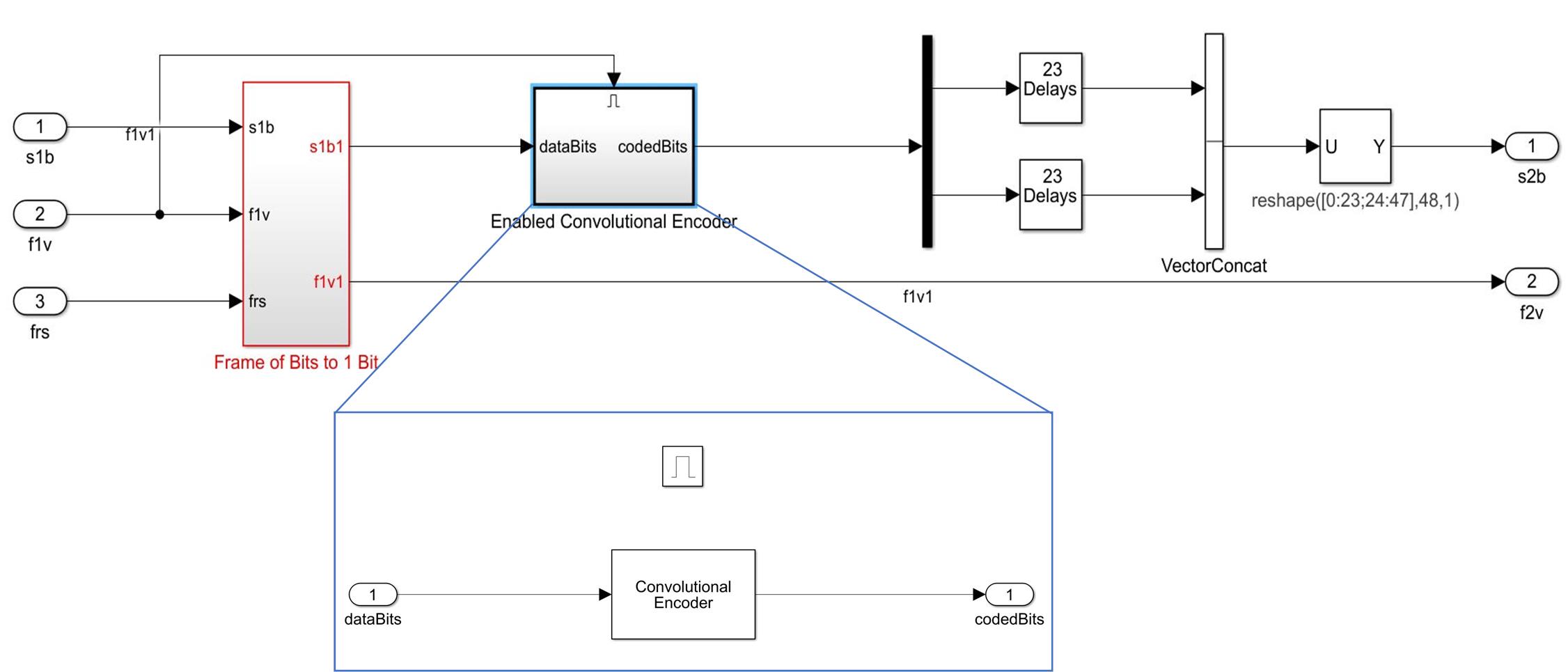
The scrambled sequence and the valid sequence are then forwarded to the convolutional encoder block. A rate convolutional encoder with and as the generator polynomials has been used to add error detection and correction capability at the receiver. The entire sequence is encoded using simulink convolutional encoder block for the PS implementation (Fig. 3). Since, the PL implementation is sample based, a frame to sample conversion is require prior to the convolutional encoder and a vector concatenation after encoding to retrieve the entire frame as shown in Fig. 4.

1.0.2 Interleaver
For the interleaver, selector block is used along with the interleaving index. The implementation is similar in both PS and PL as shown in Fig. 5.

1.0.3 BPSK Modulation
BPSK modulation used in the architecture has and as the constellation points. The pre-defined BPSK baseband modulator block of the simulink communication toolbox is used in the PS implementation (Fig. 6). The phase offset is set to zero. Similarly, other modulation schemes can also be used. We have designed our own model for PL implementation of the BPSK modulation wherein we shift the amplitude of the incoming bit to the respective constellation points using multiplication and subtraction. The complex BPSK symbols are generated by assigning the imaginary part to be zero (Fig. 7). However an HDL coder block for BPSK modulation is also available.


1.0.4 Frame Generation
As per the LDACS specifications, 64 subcarriers are used out of which 50 subcarriers are active on which data and pilots are transmitted. The number of pilots and data subcarriers depends on the symbol index. For example: The number of data subcarriers at symbol index 0 and 1 are 36 and 48 respectively, also the pilot subcarriers are 14 and 2 respectively. There are total of 54 symbols in 1 frame and symbols at indexes 0, 51, 52 and 53 have totally different pilot positions and other symbols have 5 different pilot patterns which repeats after every 5 symbols.

The architecture in Fig. 8 consists of an HDL counter to count symbol number, a Symbol Index Controller (HDL Compatible User Defined Function in Matlab), and the subcarrier mapping for different symbol indexes as major blocks. Here, the input valid signal increments the HDL counter value, and the counter counts till 53, as there are total 54 symbols in one frame. Using the counter input, which corresponds to OFDM symbol index, the symbol index controller generates nine enable signals EN1-EN9. These EN1-EN9 signals are used to enable the corresponding symbol to subcarrier mapping. We can understand this with an example, Let HDL counter gives the counter value as 1, the symbol index controller will enable the output EN5 and the EN5 will enable the subcarrier mapping designed for symbol index 1. The EN5 will also be enabled when the counter values are 6, 11, …, 46 as these symbols follows the same pilot pattern as symbol index 1. There are 7 different pilot patterns generated similar to the reference MATLAB codes shared by the German Aerospace Center (DLR) provided on https://www.ldacs.com/software/. These pilot patterns are used to map the pilots in the corresponding subcarrier mapping according to the symbol index. The subcarrier mapping is similarly designed for symbols 53 and 54, which have zeros and synchronization symbols instead of pilot symbols.
Here, we are showing the subcarrier mapping of symbol indexes 1, 6, 11, …, 46 having 48 data , two pilots positioned at and subcarrier, , 1 DC (in middle), and 13 Null subcarriers (7 left subcarrier + 6 right subcarrier position) (as shown in the appendix), and symbol indexes 3, 8, 13, …, 48 having 46 data, four pilot positioned at , , and subcarriers, 1 DC (in middle), and 13 Null subcarriers (7 left +6 right) in Fig. 9 (a) and (b) respectively.


1.0.5 Preamble Addition
The preamble sequence is predefined and has both long and short preamble sequence. For the PS implementation Fig. 10, a counter is used to detect the frame number. For the first 4 frames, the preamble (both short and long) is transmitted. The preamble sequence is read from the workspace. Of the 320 samples, 80 samples to be transmitted are selected depending on the frame number. For the PL implementation, the preamble sequence is stored in LUTs each for short and long preamble. The data and the valid signal to be transmitted are then decided depending on the sample number detected using a counter Fig. 11.


Receiver
1.0.6 Preamble Detection
The valid signal from the transmitter now enables the receiver functionality. The first step in the receiver is preamble detection which uses auto-correlation to detect the data frames. The auto-correlation is performed using a filter and a magnitude detector to detect the peak Fig. 12. The implementation of preamble detection is same in both PS and PL.

1.0.7 BPSK Demodulator
Using the simulink BPSK baseband demodulator block we retrieve the bi stream from BPSK symbols in both the PS and PL implementations as shown in (Fig. 13) and (Fig. 13). However, delays are used in the PL implementation to generate an appropriate valid signal to keep the data integrity and get the complete frame of 64 bits required for the deinterleaving process ahead (Fig. 14).


1.0.8 Deinterleaver
The bitstream is deinterleaved using the pre-defined deinteleaver sequence and a selector block similar to the interleaving process discussed above.
1.0.9 Viterbi Decoder
The viterbi decoder block from communications system toolbox is used to decode the data. For the PS implementation, the complete frame is fed to the decoder to generate the output frame consisting of the decoded bits (Fig. 17). While in the PL implementation, sample counter is used to monitor the incoming bits corresponding to each output sample bit as shown in Fig. 17.


1.0.10 Descrambler
A predefined descrambling sequence is then used to retrieve the original 24 bits using an XOR operation in both PS and PL. While no additional functionality is required in the PS, in PL the decrambler in enabled upon receiving the appropriate valid signal and input bit. Fig. 17.


next, we discuss the workflow for Hardware - software co-design approach used for the transceiver implementation.
Hardware - Software co-design workflow
To design and simulate the transceiver models Hardware - Software Co-Design approach is being used. It is an important approach to implement any algorithm on ZSoC as it utilizes the heterogeneity of PS and PL. This approach also gives the flexibility to choose which part of the system is best suited to be implemented on PL and which on PS. PS makes easy and faster decision-making operations on the other hand PL reduces power consumption and increases speed. The steps for hardware-software Co-Design approach are as follows:
- 1.
Designing a Simulink model for transceivers and set the parameters like number of samples per frame, sampling frequency, total FFT size, Active subcarriers, and subcarrier spacing. All the blocks present in the Simulink library are not hardware synthesizable. So, while designing the Simulink model these blocks need to be avoided.
- 2.
Differentiate the subsystem of the model which is going to implement on the PL believing that all the other subsystems will target to implement on PS. PL works in sample mode, and PS works in frame mode, which requires an appropriate sample to frame and frame to sample conversion at the boundary of PS-PL interface. Fig. 19 shows the design have functional blocks. Transmitter subsystem consisting of blocks are implemented on PS, and remaining blocks are implemented on PL. Similar process is used for the receiver operations. Note that, the output to the host computer will come back through the PS.
Figure 19: Hardware - Software Co-Design approach for algorithm implementation - 3.
Then, run the HDL Workflow Advisor to auto-generate an IP Core block for the transceiver design as shown in Fig. 20. It automatically generates a Vivado block diagram to combine the DUT with all the AXI interface components and creates an interface model to interact with the PL. It then uses the HDL coder and Xilinx Vivado for synthesis, implementation and bitstream generation. This bitstream is then used to program the PL.

Figure 20: Hardware-Software work flow for ZSoC using HDL and Embedded coders of Matlab/Simulink and Xilinx Vivado. - 4.
Finally, by setting the generated interface model to run in external mode, Simulink uses Embedded Coder to generate C code for all the processing blocks. Xilinx Vivado SDK then converts this C code to ARM executable code. When we run the simulation, it launches the executable on PS via Ethernet.