Scanning gate microscopy mapping of edge current and branched electron flow in a transition metal dichalcogenide nanoribbon and quantum point contact
Abstract
We study scanning gate microscopy (SGM) conductance mapping of a zigzag ribbon exploiting tight-binding and continuum models. We show that, even though the edge modes of a pristine nanoribbon are robust to backscattering on the potential induced by the tip, the conductance mapping reveals presence of both the edge modes and the quantized spin- and valley-current carrying modes. By inspecting the electron flow from a split gate quantum point contact (QPC) we find that the mapped current flow allows to determine the nature of the quantization in the QPC as spin-orbit coupling strength affects the number of branches in which the current exits the constriction. The radial conductance oscillation fringes found in the conductance mapping reveal the presence of two possible wavevectors for the charge carriers that correspond to spin and valley opposite modes. Finally, we show that disorder induced valley mixing leads to a beating pattern in the radial fringes.
1 Introduction
Transition Metal Dichalcogenides (TMDCs) are materials composed of a transition metal from the group VI (M: Mo, W, etc.) and a chalcogen (X: S, Se, Te) with the formula . Being the atomic-thick semiconductor, TMDC monolayers gained recently a lot of interest as a promising material for electronic and optoelectronic application [1] where they allow for the realization of e.g. FETs [2] and ultrasensitive photodetectors [3]. Similarly to graphene, the conduction and valence band extrema in TMDCs align in two non-equivalent and points in the Brillouin zone. This effectively gives the charge carriers an, additional to spin, degree of freedom—valley [4] which can be exploited for information processing, controlled by valley mixing [5, 6]. In addition, the absence of inversion symmetry in the monolayers results in the strong spin-orbit coupling (SOC) which breaks the spin degeneracy of the valence and conduction band near to the energy gap [7, 8] making TMDCs promising candidates for spintronics applications [9, 10]. A particularly important property of TMDCs nanostructures is the formation of edge states [11], which can exhibit magnetic properties when proximitized by a ferromagnet [12] or host Majorana bound states in proximity of a superconductor [13]. Recently, significant progress has been made in theoretical understanding of electronic transport properties of TMDCs, both in theory [14, 15] and in the experiment—thanks to the realization of locally gated nanostructures [16] and split-gate QPC devices [17, 18].
A very powerful technique, well established for exploration of quantum transport properties in two-dimensional electron gases, is the SGM conductance mapping. In this approach a charged atomic force microscope tip scans over the sample inducing a repulsive potential in two-dimensional electron gas (2DEG) and thus scatters the propagating electrons. This technique has been applied to a variety of nanodevices [19], mainly realized in semiconducting heterostructures where it allowed for mapping of the electron flow. The most prominent was demonstration of branched electron flow from a QPC [20, 21] which can be affected by mode mixing induced by Rashba SOC [22]. Most importantly, by exploiting this type of measurement the coherent nature of the electronic transport can be visualized—the electron self-interference [23, 24] results in an appearance of radial conductance fringe patterns [20, 21].
So far, SGM of monolayers was studied mainly for graphene nanoribbons [25] and QPCs [26, 27] where it allowed for demonstration states localized within the constriction [28, 29]. In the presence of the magnetic field this technique allowed for visualization of quantum Hall effect [30, 31], creation of magnetic focused electron beams [31, 32, 33] and snake states [34]. Very recently, SGM of started gathering attention with the first reports of visualization of electron flow and formation of quantum dots in micrometer-sized structures [35]. This followed the previous research that used a local probe for visualization of edge states in a few-layer FET [36] using microwave impedance spectroscopy. The latter technique was also used to visualize of current flow in a heterostructure [37].
The aim of this paper is to explain how features typical to TMDCs as the presence of edge currents, strong SOC and spin-valley splitting affects SGM mapping on an example of . We find that in a pristine ribbon the edge current can be mapped only when the Fermi energy is tuned close to the edge band bottom. On the other, hand when the Fermi energy is tuned to the conduction band, the SGM conductance mapping reveal fans of conductance due to the presence of quantized modes in the nanoribbon rather than directly depict the current distribution [38]. By mapping the electron flow from a QPC constriction we find that unlike as in a 2DEG in heterostructure, the number of branches is not solely dependent on the quantized conductance value but it is rather sensitive the intrinsic SOC strength. Finally, we investigate valley-mixing effect as probed by SGM mapping of the conductance oscillations.
This Paper is organized as follows: in Section 2 we describe the model used for calculations. The conductance mapping results of a pristine ribbon and a ribbon with QPC are presented in Sections 3.1 and 3.2 respectively. We summarize the work in Section 4.
2 Model

We consider a monolayer shaped into a nanoribbon as presented in Figure 1. To describe its electronic properties we adopt the tight-binding model that includes and orbitals of Mo and S atoms respectively [39]. To allow for a large scale calculations required for the description of SGM we perform reduction of the basis that casts the contribution of -orbitals of the S layers into symmetric and antisymmetric combinations [40, 41]. The Hilbert base of the adopted model is spanned by the vector , where the A and S indices of -orbitals correspond to antisymmetric and symmetric combinations with the respect to the -axis . The index refers to spacial directions: and superscripts and indicate the top or bottom sulfur plane.
The Hamiltonian for each spin component of the considered system reads,
| (1) |
where iterate over lattice sites, go over atomic orbital basis and and are creation operators for Mo and S orbitals respectively. The first sum corresponds to the onsite energies with the elements that read,
| (2) |
and
| (3) |
In the above we include external, position dependent potential and where equals 1(-1) for spin up (down) component.
The second and third sum in Hamiltonian (1) correspond to the hopping elements between intra- and inter-atomic orbitals respectively. The mapping of coordinates into the hopping elements is presented in the inset to Figure 1. The lattice spacing is 0.319 nm. The hopping matrices for the intra- and inter-lattice hoppings are,
| (4) |
| (5) |
| (6) |
| (7) |
| (8) |
| (9) |
| (10) |
| (11) |
| (12) |
In (2) and (3) and correspond to intrinsic SOC parameters which we choose after [42], with the modification of eV and eV which assures the meV spin-orbit splitting in the conduction band minimum of and the crossing of the conduction bands as found in [43]. We adopt the following Slater-Koster parameters given in eV units: = 3.689, = -1.241, =-0.895, = 0.252, = 0.228, = 1.225, = -0.467, =-1.094, = -1.512, = -3.560, = -6.886 [40].
In our work we consider an external potential induced in the monolayer that defines the QPC constriction modeled as a split-gate [44]:
| (13) |
with and , where and control the span of the potential in the and directions respectively and where is the parameter that controls its smoothness. We take nm, nm and nm. The resulting potential for eV is plotted in Figure 1 on the colourmap.
3 Results
3.1 Pristine zigzag wire
In the considered system, the lattice in the direction is terminated by non-equivalent atoms. At the bottom edge of the ribbon is terminated by S atoms, while on the top it is terminated by Mo atoms. Those terminations constitute two zigzag edges of the ribbon that have different electronic structure. In Figure 2 we present the band structure of a 24 nm width zigzag nanoribbon. With the arrows we denote three spin-split bands that correspond to the modes located at the Mo and S edges of the ribbon. In the top part of the figure we observe sets of bands that correspond to the current polarized in , and valleys [49]. Note that changing of the width of the ribbon does not modify the structure of the edge bands until critical width of 2 nm is reached and the edge modes start to mix.
Let us first focus on the Fermi energy range where the transport is dominated by the edge modes. In Figure 3 (a) we show conductance of the ribbon versus the tip position along the axis () and the Fermi energy in range eV. The considered ribbon is invariant in the direction and we set to zero.
In the absence of the tip the conductance is proportional to the number of current carrying modes. The lack of the energy gap in the metallic band structure of a pristine zigzag ribbon leads to nonzero conductance in the whole map. For the energy range considered in Figure 3(a) this corresponds to the current being transmitted at the edges of the ribbon – see Figure 4(f). We distinguish two main regimes in the map (depicted with violet and orange colour) where the conductance takes values and due to Kramers degeneracy. The violet colour in the map corresponds to the case when a single (Mo or S) edge is populated, while the orange colour denotes the transport through both the edges [15]. A prominent feature of the map is the stability of the conductance when the tip approaches the edges despite the fact that the current is transmitted through them. Only when the Fermi energy is tuned near the bottom of the edge bands we observe that the conductance drops by as it happens for eV and eV. For such values of the small potential perturbation induced by the tip locally lifts up the energy of the edge modes. As a result their band bottom positions above the Fermi energy which in turn blocks the transport through the S edge for eV and Mo terminated edge for eV. As a result the incoming electron is reflected completely from the depletion region generated by the tip which correspondingly lowers the conductance by the conductance quanta.
In the map we also observe a sharp peak of the increased conductance due to the bend Mo edge band at energies close to eV [see the dispersion relation in Figure 2] which results in propagation of two edge modes on this side of the ribbon.
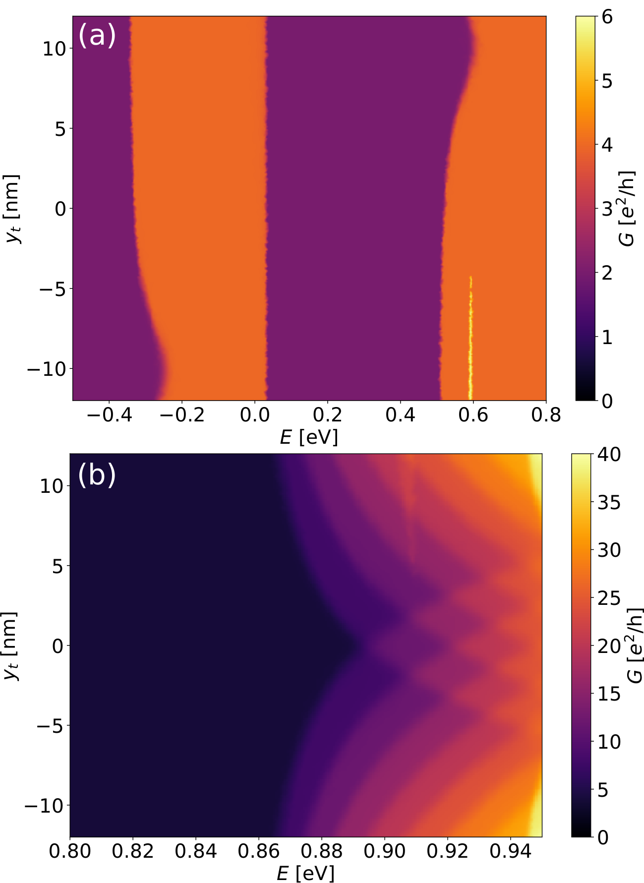
In Figure 3(b) we present the conductance map versus the Fermi energy and the tip position along the axis for the energies tuned to the conduction band. Here the current is carried mainly by the modes that have either maximum in the center of the ribbon (states with even parity) or maxima symmetrically around the center (odd states). Nevertheless, we see that actually the conductance mapping does not probe the probability current distribution, but rather we observe a set of fans of quantized conductance which increases when the tip is moved towards the edges of the ribbon—see e.g. the conductance at eV.

The above observation can be explained by an analysis of the energy bands of the ribbon section in which the tip is located. Here, the energy values are dominated by the energy separation between states of transverse quantization in the ribbon which bands we find in the top part of Figure 2. Taking a cross-section of the system at and assuming its invariance along the direction we calculate the band structure for different ’s, as we moved the tip toward the top edge, and plot it in Figures 4(a)-(d). When the tip is positioned in the center of the ribbon with we obtain the dispersion relation presented in Figure 4(a). We observe two sets of parabolas that correspond to and modes. Each band in those sets is nearly fourfold degenerate – see the red arrow in Figure 4(a). The degeneracy results from the presence of two bands split by SOC and two spatial channels for the current flow—on the two opposite sides of the tip. We show the probability current at eV in Figure 4(e), where the colors corresponds to the magnitude of the current probability. In the plot we observe the current flowing around the tip. Note that the degeneracy of the current carrying modes at the opposite sides of the tip is not perfect due to coupling to two non-equivalent edges terminated by Mo and S atoms [see the edge current flow in Figures 4(e)(f)]. When the tip is moved towards the edge of the ribbon, the band structure gradually changes as can be seen in Figures 4(a)-(d). Due to widening of the propagation channel on one side of the tip and narrowing the channel on the other side the energies of the modes propagating in the wider (narrow) channel decrease (increase). Correspondingly, the fourfold degeneracy of the bands is replaced by twofold degeneracy due presence of two spin modes – see the red arrow in Figure 4(b). As a result, subsequent bands cross the Fermi energy when the tip is moved towards the edge and accordingly the conductance gradually increases by steps.
3.2 Coherent electron flow from a QPC

The coherent electron scattering can be most distinctly demonstrated by a SGM conductance mapping of the electron flow from a QPC. Let us focus now on the conductance mapping in a ribbon with a QPC. We consider a model of a QPC in the form of a split-gate as studied in the experiment [17] with the potential plotted in Figure 1 on the colourmap. We consider a wide zigzag ribbon with the width of 200.2 nm and present in Figure 5(a) the quantized conductance versus the QPC potential for eV. For the most positive values of the gate potential in Figure 5(a) we see that the conductance reaches the value of . We have checked that this plateau is very stable in and results from the edge modes that are pinched off only if the gates create potential barrier high enough to lift up the edge mode band above the Fermi energy.
3.2.1 Branching versus SOC strength.
Let us now focus on two values for which we denote the conductance by stars in Figure 5(a). In the bottom panels we plot corresponding SGM conductance maps versus the position of the scanning probe. We observe that in the both cases the current flows in the form of a single branch. This in the striking contrast with the measurements of 2DEG in semiconductor heterostructures [50] where in absence of magnetic field, the number of branches reflects the conductance value quantized in . This is the hallmark of transmission through the QPC constriction of modes with increased quantization number and by that increased number of maxima in the cross-section of the probability current in the transverse direction.
It is important to realize here that in a bulk TMDC monolayer the conduction band minimum consists of two spin-opposite modes localized at two sets of nonequivalent and points in the Brillouin zone. At each and points there are two bands that have minima separated by the energy of stemming from the intrinsic SOC—see the inset to Figure 6. As a result, in a nanoribbon the resulting dispersion relation consist of two sets of nearly-parabolic bands for and polarized modes where in each set there are bands corresponding to spin-up and spin-down modes separated by energy of . The commonly assumed value of the spin-orbit gap of a freestanding sheet is meV as obtained from DFT calculations [43]. However, recent experiments suggest that in fact can be different, and sample dependent: in the experimental measurements of Shubnikov-de Haas oscillations in the gap value was found to be 15 meV [51]. Also, for the experimentally probed spin-orbit splitting turned out to be larger than predicted theoretically [52]. Those measurements suggest that gating and the presence of substrate might affect the magnitude of spin-orbit splitting in the conduction band. In the QPC constriction the transverse mode quantization energy of order of meV is comparable to meV. In the following we inspect how the strength of SOC affects the SGM conductance mapping by varying the value of .
To investigate the physics of the observed branched electron flow in a more detail let us approximate the monolayer band structure close to the conduction band edge at the points by the continuum Hamiltonian [43],
| (15) |
We take the effective masses: (where is the free electron mass) that corresponds to () spin-up (spin-down) bands and that corresponds to () spin-down (spin-up) bands. We neglect trigonal warping [53] and set the chemical potential eV to match the band structure obtained in the tight-binding model. is the band splitting due to the intrinsic SOC and is the valley mixing parameter. The main advantage of this model is the ability to explicitly control the strength of internal the SO coupling and the valley mixing. The resulting band structure for meV is presented in Figure 6.

We use the continuum model to describe the same system as previously treated in the tight-binding approach, i.e. we perform transport calculations describing a nanoribbon with the QPC and SGM potentials using the Hamiltonian , where is an identity matrix. We discretize the Hamiltonian on a square mesh with the lattice constant nm and apply a semi-open boundary condition analogously as in the tight-binding model case.
The obtained conductance traces versus the QPC potential are plotted in Figure 7(a) for three values of the SOC strength . For meV we find that the conductance curve depicted in panel (a) reproduces the trace obtained in tight-binging model [Figure 5(a)] differing only by the offset as the edge modes are not captured in the continuum approximation. Accordingly, when the QPC is set to the second step, there is a single branch in the conductance map of Figure 7(b) similar to the one presented in Figure 5(c).
In Figure 7(a) with the black and blue curve we plot the conductance for meV and meV. We observe that for meV when decreases the conductance raises from already to which reflects the fact that the QPC transmits three spin-degenerate modes. When we further increase to meV the overall shape of the conductance trace become again similar to the one obtained for meV. However, now mapping the current flow on the second step we observe that the current divides in two branches [Figure 7(c)]. Comparing the results for meV and meV it becomes clear that in the former case the first plateu corresponds to the transmission of two ground states of the transverse quantization with the , polarization and the value of is obtained as the QPC transmits four spin- and valley- opposite modes (, , , ) also in the ground state of the transverse excitation. For a strong spin splitting the spin-orbit split bands (, ) are shifted to higher energies and now the conductance of on the second step corresponds rather to the transmission of a ground state and an excited state of transverse quantization of two spin- and valley- opposite modes (, ). Therefore, the SGM mapping of the branched electron flow provides a tool to distinguish the nature of the conductance quantization by the QPC.
3.2.2 Oscillation period in the presence of spin- and valley-split bands.
An important feature of the conductance maps presented in Figure 5 are the radial fringes–conductance oscillations obtained when the tip moves outwards from the QPC narrowing. For a single band semiconductor they are separated by a half of Fermi wavelength and result from the interference of the wave function of the electron exiting the constriction and the wave reflected back to it [20].
To inspect the period of oscillations we consider now a modified version of the system described in the continuum model, i.e. we consider a wide (500 nm) ribbon for which we set to zero the potential created by the QPC gates for nm. This way we exclude all possible sources of back scattering for waves exiting the QPC and make sure that the QPC does not affect the local chemical potential outside the region close to the QPC gates. We consider the Fermi energy eV and meV.
In Figure 6 we plot the band structure of a bulk flake near the conduction band minimum obtained in the continuum model. At the Fermi energy of eV there are two possible values of the electron wavevector denoted with and that correspond to spin- and valley opposite modes. When the QPC is tuned to the first conductance plateau it transmits the band with minimal energy at , i.e. the one that gives the wavevector at energy 0.92 eV. Accordingly, when we inspect the conductance oscillations presented in Figure 8(a) we find that they have a period corresponding to . On the other hand, if we monitor the oscillations at the second conductance step plotted in Figure 8(b), we observe that there is no single oscillation period. In Figure 8(c) we plot conductance oscillations at the second step divided into components corresponding to the ground state in the band structure (with the wavevector at the energy 0.92 eV) [blue curve] and to the first excited state (with the wavevector at the energy 0.92 eV) [black curve]. They have two different oscillation periods and their composition gives the slightly beating curve of Figure 8(b). This is the hallmark of valley and spin coupling specific to TMDCs.
3.2.3 Beating pattern due to valley mixing.
It is important to note here that despite the electrons propagate in a composition of the two valley states there is no inter-valley scattering – the electrons are injected and exit the system in a well defined valley state. Correspondingly, each valley state exiting the QPC is interfering with its counterpart reflected from the tip. It is known that short range scatterers as vacancies in the atomic lattice [54, 55, 56] might lead to the inter-valley scattering provided the Fermi energy is high enough to allow for spin-preserving valley flips [49] and hence to mixing of the valley states propagating through the ribbon. Alternatively, the valley scattering with spin-flips can be caused by magnetic impurities [57].
Let us now investigate the effect of the valley mixing on the conductance oscillations. We first analyze the results obtained in the continuum model. In Figure 9(a) we show the conductance calculated in the continuum model with and meV with black and red curves respectively. We observe that the valley mixing induced by the nonzero parameter results in a strong beating pattern in the conductance.
Finally, we go back to the system described in the tight binding model. To test that we introduce 300 vacancies in the region span by nm and nm [58]. The resulting conductance trace is shown in Figure 9(b) with the red curve. Comparing it to the one obtained in the system with no disorder (black) we note a significant beating pattern due to valley mixing made possible now by the disorder.
4 Summary and conclusions
In summary, we have studied the electronic transport in a ribbon in the presence of a scanning probe. We adopted the the tight-binding and the continuum approaches for the description of TMDCs monolayer nanodevices. For a pristine ribbon we showed that the edge modes can be mapped by the SGM technique provided the Fermi energy is tuned to the bottom of their bands. When the ribbon is doped into conduction band the conductance probing reveals fan pattern in the conductance maps as the tip scans across the sample. This is due to the presence of the quantized spin- and valley- coupled modes in the ribbon. In wide structures where the conductance is controlled by a split-gate QPC we demonstrated that the current exits the constriction in branches which number is controlled not only by the QPC constriction itself as in ordinary 2DEGs but also by the intrinsic SOC strength. We explained that the conductance oscillation fringes evidence of two possible wavevectors for the charge carriers due to the SOC splitting of the bands. Finally, we showed that valley mixing induced by the short-range scatterers induces significant beating in the conductance oscillations.
References
References
- [1] Wang Q H, Kalantar-Zadeh K, Kis A, Coleman J N and Strano M S 2012 Nat. Nanotechnol. 7 699–712
- [2] Radisavljevic B, Radenovic A, Brivio J, Giacometti V and Kis A 2011 Nat. Nanotechnol. 6 147–150
- [3] Lopez-Sanchez O, Lembke D, Kayci M, Radenovic A and Kis A 2013 Nat. Nanotechnol. 8 497–501
- [4] Xu X, Yao W, Xiao D and Heinz T F 2014 Nat. Phys. 10 343–350
- [5] Pawłowski J, Żebrowski D and Bednarek S 2018 Phys. Rev. B 97 155412
- [6] Széchenyi G, Chirolli L and Pályi A 2018 2D Mater. 5 035004
- [7] Zhu Z Y, Cheng Y C and Schwingenschlögl U 2011 Phys. Rev. B 84 153402
- [8] Xiao D, Liu G B, Feng W, Xu X and Yao W 2012 Phys. Rev. Lett. 108 196802
- [9] Klinovaja J and Loss D 2013 Phys. Rev. B 88 075404
- [10] Han W 2016 APL Materials 4 032401
- [11] Rostami H, Asgari R and Guinea F 2016 J. Phys.: Condens. Matter 28 495001 ISSN 0953-8984
- [12] Cortés N, Ávalos-Ovando O, Rosales L, Orellana P A and Ulloa S E 2019 Phys. Rev. Lett. 122 086401
- [13] Chu R L, Liu G B, Yao W, Xu X, Xiao D and Zhang C 2014 Phys. Rev. B 89 155317
- [14] Khoeini F, Shakouri K and Peeters F M 2016 Phys. Rev. B 94 125412
- [15] Ridolfi E, Lima L R F, Mucciolo E R and Lewenkopf C H 2017 Phys. Rev. B 95 035430
- [16] Kim B K, Choi D H, Kim T H, Kim H, Watanabe K, Taniguchi T, Rho H, Kim Y H, Kim J J and Bae M H 2019 arXiv:1904.10295
- [17] Sharma C H and Thalakulam M 2017 Scientific Reports 7 735
- [18] Marinov K, Avsar A, Watanabe K, Taniguchi T and Kis A 2017 Nat. Commun. 8 1938
- [19] Sellier H, Hackens B, Pala M G, Martins F, Baltazar S, Wallart X, Desplanque L, Bayot V and Huant S 2011 Semicond. Sci. Technol. 26 064008
- [20] LeRoy B J, Bleszynski A C, Aidala K E, Westervelt R M, Kalben A, Heller E J, Shaw S E J, Maranowski K D and Gossard A C 2005 Phys. Rev. Lett. 94 126801
- [21] Jura M P, Topinka M A, Grobis M, Pfeiffer L N, West K W and Goldhaber-Gordon D 2009 Phys. Rev. B 80 041303
- [22] Nowak M P, Kolasiński K and Szafran B 2014 Phys. Rev. B 90 035301
- [23] Gorini C, Jalabert R A, Szewc W, Tomsovic S and Weinmann D 2013 Phys. Rev. B 88 035406
- [24] Kolasiński K, Szafran B and Nowak M P 2014 Phys. Rev. B 90 165303
- [25] Mreńca A, Kolasiński K and Szafran B 2015 Semicond. Sci. Technol. 30 085003
- [26] Neubeck S, Ponomarenko L A, Mayorov A S, Morozov S V, Yang R and Novoselov K S 2012 Physica E: Low-dimensional Systems and Nanostructures 44 1002–1004
- [27] Mreńca-Kolasińska A and Szafran B 2017 Phys. Rev. B 96 165310
- [28] Connolly M R, Chiu K L, Lombardo A, Fasoli A, Ferrari A C, Anderson D, Jones G A C and Smith C G 2011 Phys. Rev. B 83 115441
- [29] Garcia A G F, König M, Goldhaber-Gordon D and Todd K 2013 Phys. Rev. B 87 085446
- [30] Connolly M R, Puddy R K, Logoteta D, Marconcini P, Roy M, Griffiths J P, Jones G A C, Maksym P A, Macucci M and Smith C G 2012 Nano Lett. 12 5448–5454
- [31] Rajkumar R K, Asenjo A, Panchal V, Manzin A, Iglesias-Freire Ó and Kazakova O 2014 Journal of Applied Physics 115 172606
- [32] Morikawa S, Dou Z, Wang S W, Smith C G, Watanabe K, Taniguchi T, Masubuchi S, Machida T and Connolly M R 2015 Appl. Phys. Lett. 107 243102
- [33] Petrović M D, Milovanović S P and Peeters F M 2017 Nanotechnology 28 185202
- [34] Kolasiński K, Mreńca-Kolasińska A and Szafran B 2017 Phys. Rev. B 95 045304
- [35] Bhandari S, Wang K, Watanabe K, Taniguchi T, Kim P and Westervelt R M 2018 Nanotechnology 29 42LT03
- [36] Wu D, Li X, Luan L, Wu X, Li W, Yogeesh M N, Ghosh R, Chu Z, Akinwande D, Niu Q and Lai K 2016 PNAS 113 8583–8588
- [37] Wu D, Li W, Rai A, Wu X, Movva H C P, Yogeesh M N, Chu Z, Banerjee S K, Akinwande D and Lai K 2019 Nano Lett. 19 1976–1981 ISSN 1530-6984
- [38] Aidala K E, Parrott R E, Kramer T, Heller E J, Westervelt R M, Hanson M P and Gossard A C 2007 Nat. Phys. 3 464–468
- [39] Cappelluti E, Roldán R, Silva-Guillén J A, Ordejón P and Guinea F 2013 Phys. Rev. B 88 075409
- [40] Rostami H, Roldán R, Cappelluti E, Asgari R and Guinea F 2015 Phys. Rev. B 92 195402
- [41] Rostami H and Asgari R 2015 Phys. Rev. B 91 075433
- [42] Kośmider K, González J W and Fernández-Rossier J 2013 Phys. Rev. B 88 245436
- [43] Kormányos A, Zólyomi V, Drummond N D and Burkard G 2014 Phys. Rev. X 4 011034
- [44] Davies J H, Larkin I A and Sukhorukov E V 1995 Journal of Applied Physics 77 4504–4512
- [45] Szafran B 2011 Phys. Rev. B 84 075336
- [46] Żebrowski D, Mreńca-Kolasińska A and Szafran B 2018 Phys. Rev. B 98 155420
- [47] Groth C W, Wimmer M, Akhmerov A R and Waintal X 2014 New J. Phys. 16 063065
- [48] Nijholt B, Weston J, Hoofwijk J and Akhmerov A 2019 Zenodo. Adaptive: parallel active learning of mathematical functions. DOI:10.5281/zenodo.1182437
- [49] Gut D, Prokop M, Sticlet D C and Nowak M P 2019 arXiv:1909.13738
- [50] Topinka M A, LeRoy B J, Westervelt R M, Shaw S E J, Fleischmann R, Heller E J, Maranowski K D and Gossard A C 2001 Nature 410 183–186
- [51] Pisoni R, Kormányos A, Brooks M, Lei Z, Back P, Eich M, Overweg H, Lee Y, Rickhaus P, Watanabe K, Taniguchi T, Imamoglu A, Burkard G, Ihn T and Ensslin K 2018 Phys. Rev. Lett. 121 247701
- [52] Larentis S, Movva H C P, Fallahazad B, Kim K, Behroozi A, Taniguchi T, Watanabe K, Banerjee S K and Tutuc E 2018 Phys. Rev. B 97 201407
- [53] Kormányos A, Zólyomi V, Drummond N D, Rakyta P, Burkard G and Fal’ko V I 2013 Phys. Rev. B 88 045416
- [54] Wakabayashi K, Takane Y and Sigrist M 2007 Phys. Rev. Lett. 99 036601
- [55] Wakabayashi K, Takane Y, Yamamoto M and Sigrist M 2009 New J. Phys. 11 095016
- [56] Lima L R F, Pinheiro F A, Capaz R B, Lewenkopf C H and Mucciolo E R 2012 Phys. Rev. B 86 205111
- [57] Ávalos-Ovando O, Mastrogiuseppe D and Ulloa S E 2016 Phys. Rev. B 94 245429
- [58] The edge vacancies can significantly alter the transport properties of a ribbon when the Fermi energy is tuned into the bulk gap as found in [15]. There, the authors found that even a single edge vacancy can significantly alter the edge transport, provided that the sites close to the edges are vacant. Nevertheless, in our SGM study of the system with QPC, the conductance mapping is sensitive to the current flow from the QPC constriction – far from the edges. The disturbance of the edge transport modifies the conductance—when the edge transport is blocked—but that alters the overall conductance magnitude, not its change induced by the tip which scans the vicinity of the QPC constriction