SiPM behaviour under continuous light
Abstract
This paper reports on the behaviour of Silicon Photomultiplier (SiPM) detectors under continuous light. Usually, the bias circuit of a SiPM has a resistor connected in series to it, which protects the sensor from drawing too high current. This resistor introduces a voltage drop when a SiPM draws a steady current, when illuminated by constant light. This reduces the actual SiPM bias and then its sensitivity to light. As a matter of fact, this effect changes all relevant SiPM features, both electrical (i.e. breakdown voltage, gain, pulse amplitude, dark count rate and optical crosstalk) and optical (i.e. photon detection efficiency). To correctly operate such devices, it is then fundamental to calibrate them under various illumination levels.
In this work, we focus on the large area (1 cm2) hexagonal SiPM S10943-2832(X) produced by Hamamatsu HPK for the camera of a gamma-ray telescope with 4 m-diameter mirror, called the SST-1M. We characterize this device under light rates raging from 3 MHz up to 5 GHz of photons per sensor at room temperature (T = 25 ∘C). From these studies, a model is developed in order to derive the parameters needed to correct for the voltage drop effect. This model can be applied for instance in the analysis of the data acquired by the camera to correct for the effect. The experimental results are also compared with a toy Monte Carlo simulation and finally, a solution is proposed to compensate for the voltage drop.
1 Introduction
SiPM detectors have become the preferred photosensors for many applications in high-energy particle and astroparticle physics, and they are very attractive also for LIDAR and medical imaging applications for diagnostic and therapeutic purposes. More traditionally, such applications employ photomultipliers tubes (PMTs) or multi-anode PMTs (MA-PMTs). Between the important advantages of SiPMs there are compactness, speed of response, insensitivity to magnetic fields, high gain, and low operating voltage. Additionally, with respect to PMTs, they offer the possibility to operate under high and continuous illumination without ageing. While SiPM devices are commonly used as single photon detectors operating in dark conditions, in this study we describe how SiPM devices can be used as multi-photon detectors under continuous light (CL).
As an example application of SiPM in the presence of CL, SiPMs are now being adopted for cameras of Imaging Atmospheric Cherenkov Telescopes (IACTs) dedicated to gamma-ray astronomy. The pathfinder of this technology applied to gamma-ray astronomy has been the FACT telescope [1]. Further developments have been performed for the implementation of the Cherenkov Telescope Array (CTA) [2, 3], in the frame of which the SST-1M was originally developed [4] with its SiPM-based camera [5]. Thanks to their robustness, the CL at which SiPMs can operate is higher than for photomultipliers [6]. For IACTs, CL is due to night sky background (NSB), meaning stray light from reflections from ground and light from human induced sources, and light due the presence of high moon.
Continuous light on a SIPM sensor leads to a steady current flowing through it. To prevent such a high current to eventually damage it, a bias resistor, , is connected in series with the SiPM. This current flowing in translates into a voltage drop at the SiPM bias stage thus reducing the current. It is a typical negative feedback loop. At the same time, the affects the over-voltage, (where is the breakdown voltage and the bias voltage supplied by the power supplier PS), which impacts most of the SiPM parameters: gain (), timing, photon detection efficiency (), dark count rate (), optical crosstalk probability () and afterpulse probability (). Therefore, when SiPM devices are used in the presence of CL, all these parameters have to be characterized as a function of the impinging light intensity to correctly define the performance of a sensor. The consequence of the variation of SiPM operation parameters is that the same incoming physics signal produces a different output when observed in different CL levels. At the analysis level, the corrections for this effect must be applied to interpret experimental data properly. These corrections are important for the operation of SiPM-based gamma-ray cameras and also for applications where sensors are subject to high radiation levels, which induce an increasing dark count rate with increasing integrated dose. In this case, the dark count rate can reach such high levels to mimic CL with rates of the order of several MHz [7].
In Sec. 2 we illustrate further the behaviour of SiPM devices under CL. In Sec. 3 we describe the voltage drop process mathematically and in Sec. 4 we describe the implementation of a toy Monte Carlo (MC) for DC coupled electronics systems. After, in Sec. 5 we show the comparison of the proposed toy MC model with the simplified analytical calculation and with measurements obtained in the laboratory with a calibrated light source (Sec 5.2) and with the SST-1M camera and its Camera Test Setup (see Sec. 5.3).
2 SiPM behaviour under continuous light
In this section, we describe how SiPM devices can also be used as multi-photon detectors under CL. In this paper we focus on a DC coupled electronics associated to the SiPM.
Typical digitized experimental waveforms obtained in dark conditions and under two levels of CL are presented in Fig. 1-left, while the corresponding amplitude distribution is shown in Fig. 1-right. In dark conditions, the number of generated avalanches can be calculated by simple counting of SiPM pulses. However, above a given level of CL intensity, SiPM pulses become indistinguishable. This happens when the pulse duration of a single photon becomes compatible with the time lapse between 2 photons, i.e. the photon rate. Therefore the counting of SiPM pulses becomes impossible. Nevertheless, under high CL, can be approximated by:
| (2.1) |
where is the integral of the single p.e. pulse over its pulse length, is the waveform length and is the baseline shift calculated as:
| (2.2) |
where and are the amplitude values of the experimental waveforms for a given sample acquired with the SiPM biased above the breakdown voltage and below, respectively, and is the number of waveform samples. It is worth to mention that is dominated by the electronics baseline, while contains also both detected light pulses (if the SiPM is exposed to light) and SiPM correlated noise. Correlated noise is due to afterpulses and cross-talk. There is a given probability that an afterpulse might generate itself other afterpulses, . Therefore, following the Ref. [8], the total probability that an initial avalanche will be enhanced by afterpulses is:
| (2.3) |
Similarly, for optical cross-talk, with a given probability , this enhancement of the cascading effect leads to:
| (2.4) |
The is the number of avalanches due to the detected photons and augmented by SiPM correlated and uncorrelated noise:
| (2.5) |
where is the number of detected photons. Therefore, , can be calculated as:
| (2.6) |
and the number of photons can be calculated as:
| (2.7) |


Usually SiPMs are operated in dark conditions and therefore also and noise, namely, , and , are evaluated in dark conditions. Nonetheless, SiPMs are usually biased through a RC filter (see e.g. [9]) in order to:
- •
filter high frequency electronic noise coming from the bias source;
- •
limit the current in order to protect the sensor in case of intense illumination.
Due to the presence of the bias resistor and CL, the SiPM parameters deviate from their “dark" values, meaning their values measured in dark conditions. As a matter of fact, the voltage drop, , induced by the bias resistor reduces the over-voltage as follows:
| (2.8) |
where is the current generated by the SiPM.

From Eq. 2.8, one can conclude that the smaller is, the more stable will be the sensor response. However, having a small also means that high currents can flow through a SiPM, leading to self-heating of the sensor for high CL, as shown in Fig. 2. If there is a possibility to measure the , the can be compensated by the feedback system described in Ref. [10]. For other cases, the can be calculated analytically or from the toy MC, as shown in next sections.
3 Analytic description of the voltage drop process
The voltage drop process can be described by the scheme in Fig. 3. We adopt in the figure the already defined voltage supplied by the power supply, , the breakdown voltage and the one at the SiPM terminals . The rates of CL expressed in photons and in photo-electrons (p.e.) per unit of time are, respectively, and (where is obtained from at a certain wavelength using the ). The important input parameters for this model are:
- •
the microcell and parasitic capacitance’s, which determine the SiPM gain, , and therefore allow to convert p.e. to current;
- •
the determines the probability that a photon of a given wavelength is detected at a given over-voltage ;
- •
determines the rate of thermally generated avalanches at a given (i.e. the uncorrelated SiPM noise);
- •
The optical crosstalk probability, and the after pulse probability, (i.e. the correlated SiPM noise). Both probabilities enhance the total rate of avalanches produced by SiPM at a given ;
- •
a precise template of the typical normalized SiPM pulse due to 1 p.e. at a given temperature. The SiPM pulse template can be calculated by averaging a given number of normalized single 11 1 A single p.e. pulse is separated by neighboring pulses by a time interval longer than the sum of the typical SiPM rise and recovery times. pulses. Special care is taken in retrieving the slow component of the pulse. Even if its contribution to the total charge is small (e,g. 1%), with rates up to few GHz, neglecting it would lead to large discrepancies on the waveform baseline shift, which is used to derive the level of CL22 2 CL is provided by NSB in the case of gamma-ray cameras.. See Sec. 5.2 for more information about how to compensate for the slow component of the pulse.

Apart from , all aforementioned parameters depend on and are therefore effected by the voltage drop .
The calculation and simulation of the voltage drop requires to calculate dynamically the current generated by the SiPM:
| (3.1) |
with given by Eq. 2.8.The total rate of avalanches produced by the detected light enhanced by correlated and uncorrelated noise , is given by:
| (3.2) |
Following Ref. [11], , , and can be parameterized as:
| (3.3) | ||||
| (3.4) | ||||
| (3.5) | ||||
| (3.6) |
where is a free parameter, which depends on the SiPM type, the light wavelength and, to some extent, on the temperature; , , and are the average Geiger probabilities for external light of a given wavelength, optical crosstalk, after-pulses and dark pulses, respectively, and is the probability that a carrier is trapped and released after; is the probability that a photon is emitted and reaches the high field region of another cell and creates an electron-hole pair; is the rate of thermally generated carriers; is another free parameter describing the increase of with due to electrical field effects.
Eq. 3.1 becomes non-linear, once taking into account Eq. 2.8 and Eqs. 3.2–3.6. In order to simplify Eq. 3.1, the Taylor series expansion can be applied to Eg. 3.2-3.6. However, to achieve a reasonable agreement between the formula and the measured parameters (i.e. , , and ), the Taylor expansion needs a second or even third terms, which eventually leads to a fifth order in Eq. 3.1.
An analytical calculation of Eq. 3.1 can be done only for the simplified case that CL affects only the SiPM gain [12], while all other parameters (i.e. , , and ) are not affected. This allows to express the voltage drop as a function of the CL rate as follows:
| (3.7) |
where is the CL rate expressed in p.e. per second.
To have a precise calculation of and at the same time avoid the complexity of solving Eq. 3.1 analytically, a toy MC model is developed.
4 The toy Monte Carlo
The described model in Sec. 3 is implemented into a toy MC. In the first step, all relevant SiPM parameters are measured experimentally for the large area (1 cm2) hexagonal SiPM, S10943-2832(X), produced by Hamamatsu HPK [9] for the single mirror small size telescope SST-1M camera. All these parameters and their measurements are described in Ref. [11].
Each simulated time interval, typically between 200 and 2’000 ns, was sampled with a given sampling rate and sample time width (typically, in the interval 100 ps 4 ns). For each sample , in the range from 0 to , the main simulation steps are:
- 1.
randomly generate a number of photons using a Poisson distribution with mean value of according to the CL rate with a given wavelength distribution or single wavelength. If the simulated optical system contains wavelength filters, e.g. entrance window of the camera with anti-reflective coating and low pass filer, it can be accounted for at this stage;
- 2.
each generated photon is processed separately. It may be detected or not, depending on the and photon wavelength:
(4.1) where is a random number uniformly distributed from 0 to 1 and is:
(4.2) - 3.
on top of the CL (i.e. ), the SiPM uncorrelated noise (with rate ) is added:
(4.3) where is the number of dark pulses, calculated as:
(4.4) Here, we neglect that two or more dark pulses may appear within the same , because even for large of 4 ns this probability is less than 1%.
- 4.
are randomly enhanced by optical crosstalk and/or afterpulses. The total number of avalanches for a given sample , is then: ;
- 5.
randomly create an avalanche generation time from an uniform distribution in the range 10 ps + () ;
- 6.
is converted into the SiPM current as:
(4.5) In this step is randomly smeared with a Gaussian distribution with standard deviation corresponding to the SiPM gain fluctuation between different micro-cells;
- 7.
is used to calculate , and both are used to estimate the effect on the overvoltage in the sample :
(4.6) The overvoltage is used to derive the values of all parameters (e.g. , , , , and ) for the sample ;
- 8.
the arrival time of detected and generated photons, as well as all parameters used in the simulation, are stored in a ROOT33 3 https://root.cern.ch binary file for future use.
At the last sample , the experimental waveform is generated as the sum of all the generated avalanches convoluted with the template of the typical normalized SiPM pulse with its amplitude and shifted by the initial electronic baseline. Additionally, each waveform value is randomly smeared by a Gaussian distribution with a standard deviation corresponding to the electronic noise of the system under consideration.
To illustrate the simulation steps, the average resulting from the simulation of a SiPM illuminated with a photon rate of = 2 GHz as a function of time is presented in Fig. 4 (top) for two values of of 2.4 k and 10 k. Relatively fast changes of the main SiPM parameters, in particular of the over-voltage , and consequently of the , are observed within the first time steps of the simulation before the steady state is reached. Such a behaviour is related to recursive conjugation of and . At , increases with (see Eq. 3.1), but it is quickly quenched by the presence of the bias resistor which causes the over-voltage to decrease (See Eq. 2.8). The time interval before the steady state is achieved increases with and . For this particular example, it is reached after 100 ns.

5 Validation of the toy Monte Carlo
The proposed toy MC is compared with a simplified analytical calculation [12], and then with measurements obtained in the laboratory with a calibrated light source. It is then compared with data taken with the SST-1M camera and its Camera Test Setup (CTS) [5]. The results are described below.
5.1 Validation with the analytical calculation
As discussed in Sec. 3, the analytical calculation of voltage drop can be done assuming that CL affects only the SiPM gain . To compare this analytic expression with the proposed toy MC, the voltage drop is simulated using real SiPM parameters and using a simplified case. For this simplified case, we use the toy model assuming null values for , and and that the is 100%. The results for (full symbols) and 2.4 (empty symbols) are presented in Fig. 5. Independently of , the comparison between the analytical expression (lines) and the simplified model (squares) shows an excellent agreement. The relative difference is less than 0.5% on average. When compared to the full model (circles), the relative difference increases to an average of 14%, which is expected due to the assumed simplifications to use the analytical expression.

5.2 Validation with calibrated light sources
For this study, the experimental setup at IdeaSquare44 4 http://ideasquare.web.cern.ch at CERN was used, and is illustrated in Fig. 6. The full description of the set-up may be found in [11]. The SiPM is biased with a Keithley 2410 through an RC filter ( = 10 k, = 100 nF). The SiPM anode is connected to the Keithley Picoammeter 6487 to measure the bias voltage at the SiPM and also to the preamplifier board developed for the SST-1M camera (more details can be found in [12, 5]). The waveform readout is performed with a Lecroy 620Zi oscilloscope. The set-up is equipped with two LEDs ( = 470 nm each). A LED is pulsed in mode (to emulate the flashes of Cherenkov light induced by atmospheric showers), while the other is continuous, or in the so-called mode (to emulate the NSB or CL). The SiPM under study was biased to = 58 V and temperature of 25 , corresponding to V. For each light level, 10’000 waveforms are acquired, each of 2 s long (5’000 samples per waveform). The light intensity is monitored with precision using a calibrated photodiode55 5 Hamamatsu S1337-1010BQ, s/n 61.
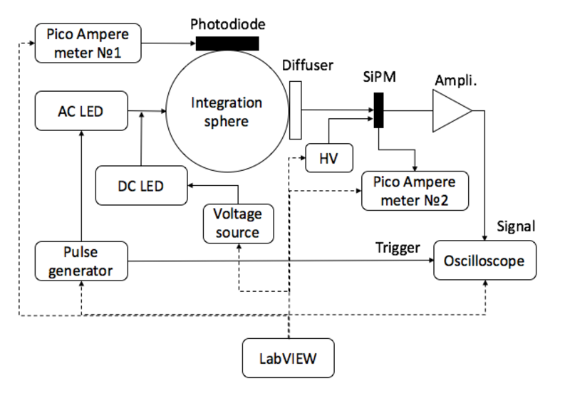
Two types of measurements were performed, as described next.
DC scan
The first measurement is performed with different CL levels. The LED in continuous mode is used to emulate the various CL levels. The measured and average waveform baseline are compared with simulated values. Fig. 7-left shows a good agreement between the measured and the simulated as a function of in terms of photons/s (the number of photons can be extracted using the calibrated pohotodiode). However, the measured baseline shift is almost two times higher with respect to the simulated one (see Fig. 7-right).


The difference in baseline shift can be explained by the slow pulse component (referred to as “DC pulse component”), which extends over 150 ns. This DC pulse component is not included directly in the toy model, as the adopted pulse template is only 150 ns long. The DC pulse component is difficult to measure because of the high and in this large SiPM area (93.6 mm2). Therefore, the DC pulse component is measured using low rates of injected light ( MHz). This light level is chosen to fulfill two requirements:
- •
single SiPM pulses are still distinguishable 66 6 A single pulse is a SiPM signal separated by the neighboring pulses by a time interval higher than , where and are the typical SiPM recovery and rise times, respectively, and = 40 ns is the time interval during which the local baseline calculation is performed.;
- •
the , used to convert into can be considered constant77 7 We estimated a relative drop of 1.75 for = 120 MHz..
For each pulse, the local baseline is calculated within 40 ns before the pulse. The deviation of the local baseline, at a given level, from its value in the dark is called in the following “local baseline shift”: . The is converted from a voltage into a charge as:
| (5.1) |
where is the waveform duration and is the load resistance. At the same time, is converted from number of photons into SiPM detected charge as:
| (5.2) |
The average as a function of the is presented in Fig. 8. We can see that the increases linearly with with a slope of . This slope indicates that only 32.3% of the charge generated by the SiPM is seen as a pulse, while the remaining 67.7% goes into the baseline shift. Implementing this behaviour inside the toy MC dramatically increases the simulation time. Therefore, the effect is accounted for some additional steps after the simulation is performed. As a matter of fact, each simulated waveform is shifted by an additional baseline , calculated as:
| (5.3) |
where is the total current generated by the SiPM within the simulated waveform. The results obtained accounting for this additional baseline shift are presented in Fig. 7 (right) with solid lines and indicated as “DC pulse component” in the legend.

AC/DC scan
The second measurement is performed with different pulsed and CL levels. The average waveform amplitude, , and average waveform baseline, , corresponding to the AC LED, depend on due to the voltage drop effect. The variation with respect to the case without CL can be calculated as:
| (5.4) |
where and are the average amplitude and average baseline, respectively, at a given DC LED intensity, while and are corresponding values at zero DC intensity. As shown in Fig. 9-left, we can observe that the detected pulse amplitude after baseline subtraction decreases with increasing DC LED intensity, as it is expected due to . This behaviour was compared with the results from the toy model for of 85 and 95 fF. We can observe that the maximum difference between measured and simulated values, for fF, is less than 5%.
Typically, during the operation of SiPMs in real conditions, the CL level is unknown. However, it can be calculated from the baseline shift or its standard deviation. For these purposes the relative amplitude, , as a function of the baseline shift is presented in Fig. 9-right.


5.3 Validation with the Camera Test Setup
Further measurements are performed with the SST-1M camera [5] and its camera test setup (CTS), at the University of Geneva. The CTS calibration tool, described in Ref. [5], is equipped with two LEDs ( = 468 nm) corresponding to each SST-1M camera pixel: one in pulsed mode ( LED) and the other in continuous mode ( LED). With the CTS, the scan described in Sec. 5.2 is done for all 1296 camera pixels at = 2.8 V. For each pixel, AC and DC LED values, the baseline and signal amplitude are calculated. The relative amplitude (see Eq. 5.4) as a function of the baseline shift is presented in Fig. 10. We can observe that almost for all pixels decreases with increasing baseline shift (i.e. CL). Few pixels do not follow this tendency as either the pixel itself or the LEDs facing it were found to be faulty. In addition, some LEDs have a higher intensity with respect to others resulting in the saturation of the pixel readout chain [12]. Therefore, no drop of is observed. The relative difference between data and the proposed model is shown in Fig. 10 (bottom). It is around 5%, confirming the results shown in the previous section.

6 Results
From the proposed toy model, the CL level and the can be obtained from the baseline shift or its standard deviation. Therefore, all SiPM parameters can be corrected according to , as shown in Fig. 11 for the , and the amplitude of the single p.e. signal. By comparing the relative drop of the main SiPM parameters with CL for of 10 k and 2.4 k we can conclude that for of 2.4 k the relative drop is more than three times smaller, because is proportional to (See Eq. 2.8). Hence, low values of simplify operation of SiPM under CL. A similar plot can be obtained in photons/s when the effect of and additional optical elements (light guides, window, etc.) are included in the simulation.


The drop of the SiPM parameters (See Fig. 11) under CL may be compensated by increasing the bias voltage by some correction voltage in order to keep constant the over-voltage (see Eq. 2.8). We call this “compensation loop”. is determined from the toy MC. As an example, the evolution of and with time under CL of photons/s is shown with compensation loop (dashed lines) and without (solid lines) in Fig. 12 (top). We can observe that, to compensate by V, the should be increased by 1.7 V, as shown in Fig. 12 (bottom). As a drawback, the detected NSB rate increases from up to . Hence, the SiPM power consumption increased from 5.17 mW up to 10.29 mW.


The as a function of baseline shift is presented in Fig. 13 for two values of of 10 k and 2.4 k. We can observe that increases linearly with increasing baseline shift with a slope of 13.47 and 3.23 for of 10 and 2.4 k, respectively. Therefore, in experimental conditions, when CL is known and stable in time, the effects from can be corrected. As a drawback, the SiPM power consumption increases after compensation loop activation, as shown in Fig. 13. Also, the baseline standard deviation can be used to calculate . However, it is less precise since shows stronger dependence on statistics and electronic noise.


7 Conclusions
In this paper we report on the studies of SiPM behaviour under CL. A Toy Monte Carlo model was developed for DC coupled electronics. This model is used to predict the behaviour of all relevant SiPM parameters (i.e. Gain, Photon detection efficiency, optical crosstalk, after-pulses, dark count rate and etc.) under various CL. The model is validated by comparison with experimental data measured for a single SiPM as well as for the full SST-1M gamma-ray camera, which contains 1296 SiPM devices. This model can be adapted to any DC coupled SiPM. Indeed, it can also be extended to the AC coupling case. As a matter of fact, in [5] it can be seen that the standard deviation of the waveform also increases with increasing CL. This parameter can therefore be used as an indicator for AC coupled systems, similarly to the baseline shift that we used for DC coupling. However, we showed that a DC couple system is preferable as the standard deviation tends to saturate at large CL levels while the baseline shift does not.
References
- [1] H. Anderhub, et al., Design and Operation of FACT – The First G-APD Cherenkov Telescope, JINST 8 (06) (2013) P06008–P06008. doi:10.1088/1748-0221/8/06/p06008.
- [2] CTA Observatory, https://www.cta-observatory.org/.
- [3] B. S. Acharya, et al., Science with the Cherenkov Telescope Array, WSP, 2018. arXiv:1709.07997, doi:10.1142/10986.
- [4] T. Montaruli, The small size telescope projects for the Cherenkov Telescope Array, PoS ICRC2015 (2016) 1043. arXiv:1508.06472, doi:10.22323/1.236.1043.
- [5] M. Heller et al., An innovative silicon photomultiplier digitizing camera for gamma-ray astronomy, The European Physical Journal C 77 (1) (2017) 47. doi:10.1140/epjc/s10052-017-4609-z.
- [6] D. Neise, et al., FACT - Status and experience from five years of operation of the First G-APD Cherenkov Telescope, Nucl. Instr. Meth. A 876 (01 2017). doi:10.1016/j.nima.2016.12.053.
- [7] E. Garutti, Y. Musienko, Radiation damage of SiPMs, Nucl. Instrum. Meth. A 926 (2019) 69 – 84, silicon Photomultipliers: Technology, Characterisation and Applications. doi:https://doi.org/10.1016/j.nima.2018.10.191.
- [8] A. Para, Afterpulsing in Silicon Photomultipliers: Impact on the Photodetectors Characterization (2015). arXiv:1503.01525.
- [9] Hamamatsu web site, https://www.hamamatsu.com, accessed: 2019-02-07.
- [10] A. Biland, et al., Calibration and performance of the photon sensor response of FACT — the first G-APD Cherenkov telescope, Journal of Instrumentation 9 (10) (2014) P10012–P10012. doi:10.1088/1748-0221/9/10/p10012.
- [11] A. Nagai, et al., Characterization of a large area silicon photomultiplier, Nucl. Instr. Meth. A 948 (2019) 162796. doi:https://doi.org/10.1016/j.nima.2019.162796.
- [12] J. Aguilar, et al., The front-end electronics and slow control of large area SiPM for the SST-1M camera developed for the CTA experiment, Nucl. Instrum. Meth. A 830 (2016) 219 – 232. doi:https://doi.org/10.1016/j.nima.2016.05.086.