ROBUST BGA VOID DETECTION USING MULTI DIRECTIONAL SCAN ALGORITHMS
Abstract
The life time of electronic circuit’s board are impacted by the voids present in soldering balls. The quality inspection of solder balls by detecting and measuring the void is important to improve the board yield issues in electronic circuits. In general, the inspection is carried out manually, based on 2D or 3D X-ray images. For high quality inspection, it is difficult to detect and measure voids accurately with high repeatability through the manual inspection and it is time consuming process. In need of high quality and fast inspection, various approaches were proposed for void detection. But, lacks in robustness in dealing with various challenges like vias, reflections from the plating or vias, inconsistent lighting, noise, void-like artefacts, various void shapes, low resolution images and scalability to various devices. Robust BGA void detection becomes quite difficult problem, especially if the image size is very small (say, around 40x40) and with low contrast between void and the BGA background (say around 7 intensity levels on a scale of 255). In this work, we propose novel approach for void detection based on the multi directional scanning. The proposed approach is able to segment the voids for low resolution images and can be easily scaled to various electronic manufacturing products.
Keywords Soldering ball, Void detection, Image processing, Computer Vision, Deep Learning
1 Introduction
In the electronic circuits manufacturing, a type of surface-mount named soldering ball grid array (BGA) is being used widely. Due to various reasons the voids will appear in these soldering balls that will reduce the life time of the device. Inspecting the quality of BGA to confirm the presence of voids is vital for quality inspection and to reduce the cost of manufacturing and increase the life time of device. Hillman et al. 2011. In general, 2D and 3D X-ray imaging is used and voids are segmented based on the intensity differences within the BGA. Due to the low contrast between the voids and the BGA, it is difficult to accurately segment the void and an human expert is needed for the reliable inspection. The issue with the human inspection is the low repeatability due to the perceptual differences. As the number of soldering balls in BGA ranges from 10s to 100s, each ball is to be inspected in serial fashion resulting in longer inspection time. Due to these challenges in manual inspection, there is a need for robust void detection approach that can be scaled to all 2D X-ray acquisition device type, product type, layout of BGA and the void characteristics.
The above technique is helping in more robust void detection even for low contrast small size BGA images.
Image processing techniques are usually applied for void detection by segmenting each soldering ball and segmenting the void regions within each soldering ball. The arrangement, size, intensity and number of soldering balls will vary for different devices. The challenging factors in void segmentation are relative intensity of voids, vias, plated-through holes, reflections from the plating or vias, inconsistent lighting, background traces, noise, void-like artifacts, and parallax effects. There is a need of robust techniques that are able to segment soldering balls and voids considering all the mentioned factors. Although many techniques are proposed since many years, but lacks in the robustness in dealing these various challenges. The drawbacks of these approaches are scalability to new device types or different void characteristics and the parameters has to be tuned manually for different device and material types.
In Said et al. 2012, Laplacian of Gaussian (LoG) is applied to detect edges, via extraction, filtering out false voids and finally detect real voids. In Peng and Nam 2012, blob filters with various sizes are applied to segment the voids of various sizes. In Mouri et al. 2014, void detection is formulated as the matrix decomposition problem by assuming that void as sparse component and non-negative matrix factorization approach is used to separate the void region from soldering ball.
The end to end void inspection process can be broadly split into two steps. In the first step, the soldering balls are segmented from the input image and in the second step, the voids are to be segmented and analysed for each soldering ball.
Soldering Ball Segmentation
In the first step, thresholding or background subtraction techniques are usually applied to remove the background, that works well to separate out the soldering balls from background. Some of the soldering balls are not detected due to shadowing of other components. In these cases, reference ball based matching technique is applied in Said et al. 2010. Where, the reference template is used to match all the locations in the neighbourhood of occluded soldering ball. The best matched location is considered as the location of occluded one. In general, the pattern or arrangement of soldering balls will vary for each manufacturing device, prior information about the soldering balls pattern can simplify the soldering ball segmentation. To solve the pattern issue various approaches are proposed in Said et al. 2010.
Void Detection
The challenging factors in void segmentation are relative intensity of voids, shape of void, vias, plated-through holes, reflections from the plating or vias, inconsistent lighting, background traces, noise, void-like artifacts, and parallax effects. The non-void soldering balls are of uniform intensity and voids are brighter with respect to intensity of non-void soldering ball.
Various approaches are proposed in the literature to segment the voids. In Said et al. 2010, multiple tools are applied to deal with the vias and false voids. In Peng and Nam 2012, blob filters with various sizes are applied to segment the voids of various sizes. In Mouri et al. 2014, void detection is formulated as the matrix decomposition problem by assuming that void as sparse component and non-negative matrix factorization approach is used to separate the void region out of the BGA.
The shape of voids are assumed as circular in Said et al. 2010 to simplify the detection. But, in practical, the voids can be of regular and irregular shapes and the overlapping of multiple regular voids will look as irregular void. The issue with the irregular shapes is difficulty in distinguishing the irregular shape voids and overlapping voids. Normally, multiple voids will appear. In some cases, the voids are partially or totally obscured by vias and the characteristics of via reflections are similar to those of the actual voids. The challenges are the scalable robust void segmentation irrespective of shape, number of voids, overlapping between multiple voids, and noises.
In some manufacturing devices, the size of the soldering ball is less (at most 40x40) and the captured images are noisy. Although various approaches are proposed, but lacks the robustness in detecting the voids. Common approach is to join the opened contours in detected Laplacian of Gaussian (LoG) edges by considering the nearest open edges. In the case of noisy images, low resolution soldering ball images the noisy edges will be appearing regularly. In this scenario, it is difficult to find the real voids by joining the nearest edges. The noisy images will create many open edges and difficult to find the real edges to join. The edge detection based approach doesn’t consider the region characteristics to find the real voids, as the edges only consider the dissimilarity information between the neighbors.
To improve the void detection, we propose the novel approach by considering the regional information by applying multi directional scanning algorithms. The LoG detected edges are scanned in radial direction for processing to find the 1D void regions and the 1D void regions are connected to form 2D voids based on neighbors and intensity of voids. Finally, connected component is applied to get the individual voids.
The paper is organized as follow. The proposed approach is described in section 2, experimental results are presented in section 3 and finally concluded in section 4.
2 Proposed Approach
2.1 Segmentation of Soldering Balls
Given an input image, Said et al. 2010 applied adaptive thresholding to detect soldering balls and interpolating the soldering balls shadowed by the other components. The template matching approach is used to detect the soldering balls shadowed by other components. The reference soldering ball is used to match all the locations in the occluded region. The location having the higher correlation is considered as the center of the occluded soldering ball. In this work, we follow the similar steps with some modifications. Instead of considering entire image for adaptive thresholding, adaptive thresholding is applied for each slice independently to overcome the sensitivity of adaptive thresholding on non-uniform illumination and other components. We observed that after thresholding, there are some extra detections around the circle. Circles detection technique is applied to improve the robustness on these noises. Location based technique is applied to verify the detection and to interpolate the location of missing ones. If any one of them is not detected then the distance between the neighboring balls will be more compared to the reference distance. We interpolate the location of this using the information of neighboring soldering balls. The pseudo code of the proposed algorithm is described below and the flow chart is given in Fig. 1.
2.2 Void Detection
The overall flow for void detection is shown in Fig. 2
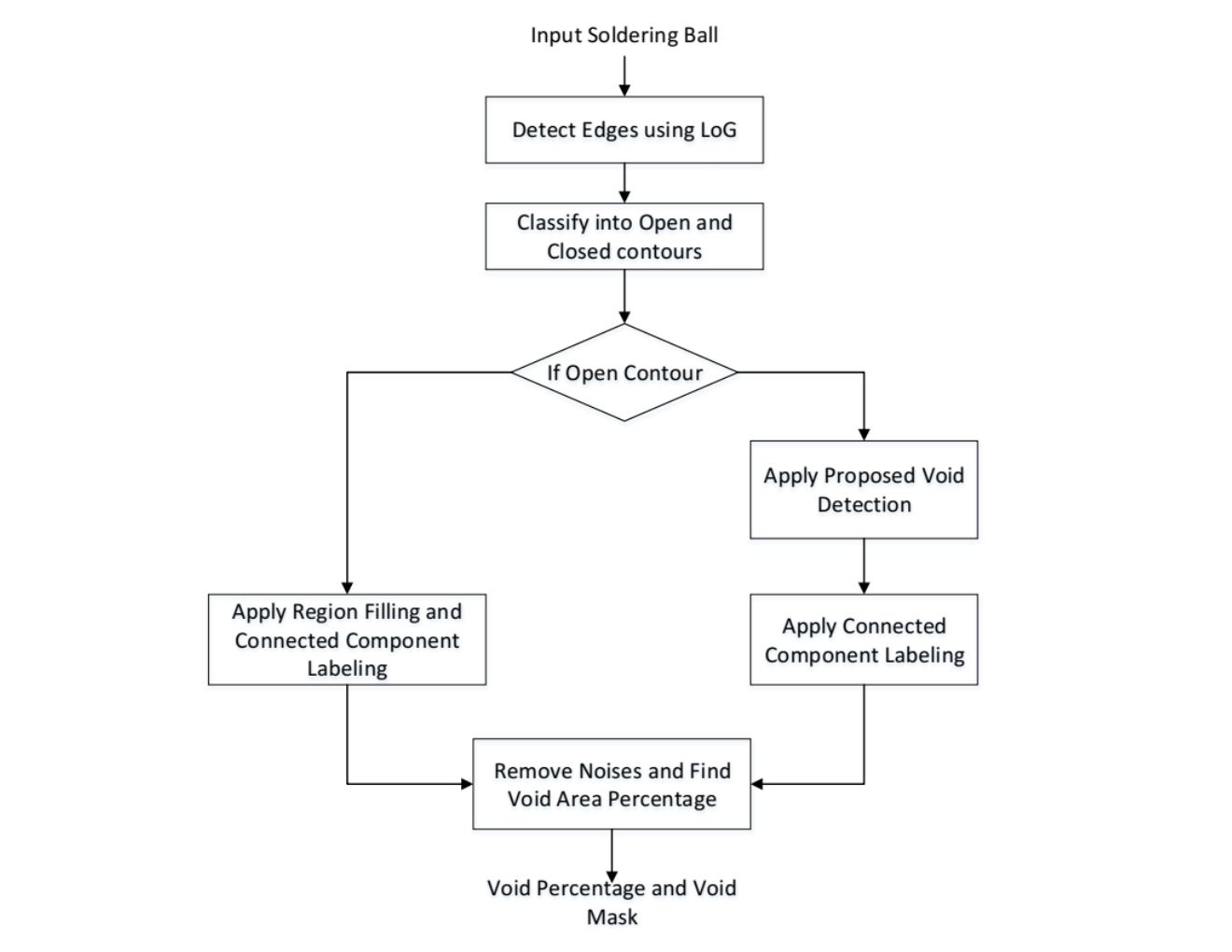
2.2.1 Detect Edges
After extracting soldering balls, the next step is to get the edges for each soldering ball. In this work, we apply LoG to detect the edges. Fig. 4 shows the detected edges using LoG for sample images.
2.2.2 Contours Classification

The edges corresponds to the dissimilarity between the two regions. In the case of noisy or low resolution soldering balls, it is possible to get many false positive edges. Fig. 4 shows the detected edges using LoG, and there is a high possibility of getting many false edges, open contours and it is difficult to filter out the false edges and close the contour to form the void region. In reference approaches Said et al. 2010, the opened contours are joined to form closed contours by finding the nearest edge points. There are no explicit steps to filter the false edges and find the original void locations. In this work, the invalid edges are filtered out by considering the region information between this edge pixel and the next consecutive edge pixel scanned in particular order. The advantage of the proposed approach is filtering false edges and finding the 1D void regions can be done in a single step. Given the input image and LoG mask, the edges are divided into open and closer contours. For closed contours, regions are filled to get the void segment. The open contours are processed using the proposed method to form void regions. The void detection approach consists of two stages 1D Void generation and 2D void generation. The flow chart of the void approach is shown in the Fig. 3.
2.2.3 Generate 1D Voids
For each pixel belonging to the positive edge (background to void), the pixels are scanned in predefined order to find the negative edge (void to background). The pixels in scanned region are used to classify it whether the region belongs to void or background. The regular scanning techniques that can be used are horizontal, vertical, radial and angular directions as shown in Fig. 5. The core idea here is to explore the efficient scanning techniques for finding void. Horizontal and vertical are the regular scanning techniques used in images. The alternative scanning approaches applied here are in radial and angular direction. The first advantage of scanning in and direction is the relatedness of circular scanning and the circular appearance of voids. In the case of low resolution soldering balls, it is difficult to distinguish the voids near the boundary. The intensity variations near the border are due to presence of void or due to edges of soldering balls. It is difficult to distinguish the void in this case using horizontal and vertical scanning. In circular and radial scanning, the intensity values are uniform at each radius r and the only intensity variations are due to void. In this case, , is considered to be effective scanning approach compared to the horizontal and vertical scanning for void detection. For each radius from (r= to 1), pixels are scanned in angular direction for processing. rmax is the maximum radius of the soldering ball. The flow chart of the 1D void detection is shown in Fig. 6.


At a particular radius r, cyclic shift is applied to find the pixel location which is a positive edge (transition from background to void). To do that, neighboring pixels ((r, -1), (r, )) are considered for checking the condition. If the intensity values at ((r, -1), (r, ), (r, +1)) are found to be in increasing order and (r, ) is an edge then edge at (r, ) is positive edge. The pixel at (r, ) is considered as starting location and the locations are scanned in angular direction until we find the negative edge (transition from void to background). The scanned locations which are in between the positive edge and negative edge are marked as void. Instead of blindly marking them as void pixels, one more extra condition that we applied is based on the maximum, minimum and average of intensity values of scanned locations. The intensity values in between the positive and negative edge are to be greater than background for a void. So, if the average value and the absolute value of maximum and minimum intensity difference are greater than (=6) then the locations are marked as void. This procedure is repeated for each radius from r = to 1.
2.2.4 Generate 2D Voids

The detected partial voids (1D voids) belonging to same 2D void are to be assembled together. Fig. 7 shows the flow chart of 2D void detection. Starting from the maximum radius r = , the 2D voids are initialized. The radius is decreased (r = -1). Each 1D void in added to the one of the initialized 2D voids, if the connectivity condition is satisfied. New 2D void is created if the condition is not satisfied. The 2D voids are terminated, if none of the 1D void doesn’t satisfy the condition. The condition to check the connectivity is pixels belonging to 1D and 2D voids are to be 8-connected and the average intensity of 2D void and the 1D void has to be same. This process is repeated for all radiuses from to 1.
2.2.5 Filtering and Void Area Calculation
After connecting the 1D voids to form 2D voids, connected component labelling is applied to separate the each void region. Regions whose area is less than minimum area ( = 9 pixels) are filtered out to eliminate the noises. In 8-connectivity, the number of pixels covered with distances 1 and 2 are 1 and 9 pixels. Number of pixels 9 is considered as the minimum area for a valid void. The percentage of void is calculated based on the void percentage and the area of soldering ball. Void area is calculated by summing up number of pixels predicted as void. The area of soldering ball is calculated as the number of pixels inside the soldering ball. The percentage of void area with respect to soldering ball is calculated as
Percentage of Void (%) = (Area of voidArea of soldering ball) *100
3 Experimental Results

Fig. 8 Shows the sample images of soldering balls and the detected voids using reference and proposed. The first image in each box represents the input image. The second and third represents the voids detected using reference and proposed. The numbers on the top of each image represents the void percentage. Compared to the reference approach, the proposed is able to detect more voids and no void will be missed. Due to the noisy edges, the reference approach is unable to fill the open contours. Whereas the proposed approach is able to scan using multidirectional scanning approach to form void regions.
4 Conclusion
The quality inspection of BGA by measuring the voids is vital for board yield issues. Various traditional approaches were proposed for void segmentation but lacks in scalability and provides less accuracy. In this paper, we applied a novel approach for void segmentation by considering the regional information by applying multi directional scanning algorithms. The LoG detected edges are scanned in radial direction for processing to find the 1D void regions and the 1D void regions are connected to form 2D voids based on neighbors and intensity of voids. The proposed approach is able to detect more voids compared to the reference approach.
References
- Hillman et al. [2011] Dave Hillman, Dave Adams, Tim Pearson, Brad Williams, Brittany Petrick, Ross Wilcoxon, Rockwell Collins, Cedar Rapids, John Travis, Vineeth Bastin, and Nordson Dage. The last will and testament of the bga void. 2011.
- Said et al. [2012] Asaad F. Said, Bonnie L. Bennett, L. Karam, Alvin Kuok Lim Siah, Kevin Goodman, and J. S. Pettinato. Automated void detection in solder balls in the presence of vias and other artifacts. IEEE Transactions on Components, Packaging and Manufacturing Technology, 2:1890–1901, 2012.
- Peng and Nam [2012] Shao-Hu Peng and Hyun Do Nam. Void defect detection in ball grid array x-ray images using a new blob filter. Journal of Zhejiang University SCIENCE C, 13:840–849, 2012.
- Mouri et al. [2014] Motoaki Mouri, Yoichi Kato, Hiroshi Yasukawa, and Ichi Takumi. A study of using nonnegative matrix factorization to detect solder-voids from radiographic images of solder. 2014 IEEE 23rd International Symposium on Industrial Electronics (ISIE), pages 1074–1079, 2014.
- Said et al. [2010] Asaad F. Said, Bonnie L. Bennett, Lina J. Karam, and Jeffrey S. Pettinato. Robust automatic void detection in solder balls. 2010 IEEE International Conference on Acoustics, Speech and Signal Processing, pages 1650–1653, 2010.