Robust magnetotransport in disordered ferromagnetic kagome layers
with quantum anomalous Hall effect
Abstract
The magnetotransport properties of disordered ferromagnetic kagome layers are investigated numerically. We show that a large domain-wall magnetoresistance or negative magnetoresistance can be realized in kagome layered materials (e.g. Fe3Sn2, Co3Sn2S2, and Mn3Sn), which show the quantum anomalous Hall effect. The kagome layers show a strong magnetic anisotropy and a large magnetoresistance depending on their magnetic texture. These domain-wall magnetoresistances are expected to be robust against disorder and observed irrespective of the domain-wall thickness, in contrast to conventional domain-wall magnetoresistance in ferromagnetic metals.
Introduction. Racetrack memory Parkin et al. 2008 has been expected to be a new generation spintronics memory device, which consists of a ferromagnetic wire with magnetic domains corresponding to “0” and “1”. Those domains can be driven by electric current and be read out rapidly without mechanical heads. The most prominent advantage of spin memories is that the device does not need electricity to keep information as conventional random access memories. That is, the racetrack memory can become a low-power-consumption device. However, this ferromagnetic metal spintronics device is not practically realized yet, in contrast with magnetic tunnel junction devices using the giant magnetoresistance effect Parkin 1995, which have achieved great success. The problem is that a current driven device of ferromagnetic metals suffers from Joule heating. In this paper, we propose that we may overcome this difficulty by using the quantum anomalous Hall (QAH) Haldane 1988; Chang et al. 2013 or Weyl semimetal Wan et al. 2011; Burkov and Balents 2011 state of kagome layered materials. In those topological states, domain walls can be driven by the electric field Upadhyaya and Tserkovnyak 2016; Araki et al. 2016; Kurebayashi and Nomura 2019; Kim et al. 2019. Therefore a large electric current that causes Joule heating is not necessary. We show, via a numerical simulation of transport, that the current is strongly suppressed by domain walls in QAH kagome layers.
In ferromagnetic metals, the domain-wall magnetoresistance (DWMR) effect originates from the spin mistracking of the conduction electrons Kent et al. 2001; Maekawa et al. 2012. Therefore the DWMR is fragile against a gradual change of magnetization (thick domain walls) or disorder, and is a weak effect compared with the widely utilized giant magnetoresistance effect Yavorsky et al. 2002. Nevertheless, the DWMR in magnetic Weyl semimetals Hirschberger et al. 2016; Wang et al. 2016; Jin et al. 2017 has been found to become huge in thick domain walls and robust against disorder Ominato et al. 2017; Kobayashi et al. 2018. Recently, it was proposed that the QAH state can be realized in kagome layered materials: Fe3Sn2 Ye et al. 2018; Yin et al. 2018, Co3Sn2S2 Liu et al. 2018; Muechler et al.; Yin et al. 2019; Ozawa and Nomura; Liu et al. 2019, and Mn3Sn Nakatsuji et al. 2015; Yang et al. 2017; Ito and Nomura 2017. In order to utilize these materials for novel topological spintronics devices, we reveal the mechanism and robustness of the DWMR in kagome layers.
In this paper, we propose a huge DWMR effect in ferromagnetic kagome layers under disorder. We first study the transport property with in-plane or out-of-plane magnetizations. Next we show the magnetization angle induced topological phase transition. Then we investigate the DWMR for various types of domain wall. We show that the DWMR is robust against disorder and hardly suppressed by thick domain walls. These results imply that the DWMR comes from the topological transport in kagome layers.

Model. We employ a single-layer kagome lattice (see Fig. 1) model with ferromagnetic order. The tight-binding Hamiltonian is,
| (1) |
The first term is the nearest-neighbor hopping. The second term is the spin-orbit coupling conserving -component of electron spin Kane and Mele 2005; Guo and Franz 2009, where and is the unit vector connecting the sites and , with the site in between next-nearest sites and . The third term is the spin-exchange coupling with local magnetization . The magnetization comes from localized spins for high-spin systems (e.g. Fe3Sn2 Caer et al. 1978; Ye et al. 2018; Yin et al. 2018) and from the mean field of itinerant spins for low-spin systems (e.g. Co3Sn2S2 Liu et al. 2018; Ozawa and Nomura). The fourth term is the on-site random potential (non-magnetic disorder), which is uniformly distributed in . Pauli matrices represent the spin degree of freedom. We take the hopping parameter as the energy unit and the distance between the nearest-neighbor sites as the length unit. The strength of the spin-orbit coupling is set to in the following.
We consider straight-edged nanoribbons of the kagome layer (Fig. 1), with length , and width . We calculate the two-terminal conductance (in units of ) between the terminals attached on the ends of the ribbon, and , by using the recursive Green’s function method Ando 1991. Since we found that the system size dependence is not important for the qualitative behavior of DWMR, we show only the data for here.

Two-terminal conductance. We first study the transport with uniform magnetization. Without magnetization, the kagome lattice system shows a quantum spin Hall state Guo and Franz 2009, similarly to the honeycomb lattice with spin-orbit coupling. Under strong spin-exchange coupling, qualitatively different behavior arises depending on the magnetization direction [Figs. 2(b) and 2(c)]. For out-of-plane () magnetizations, the system shows the QAH states, where quantized conductance arises due to the chiral edge states. (Note that the quantum spin Hall state survives for a small because the term does not break the symmetry of the Hamiltonian.) In contrast, for in-plane ( or ) magnetizations, the system tends to be “diffusive”: metallic in the clean limit and insulating in the presence of disorder, due to the Anderson localization (see Fig. 3). We can switch the type of transport, QAH and diffusive, by tilting the magnetization Kandala et al. 2015; Kou et al. 2015, and the difference is significantly contrasted in the presence of disorder.
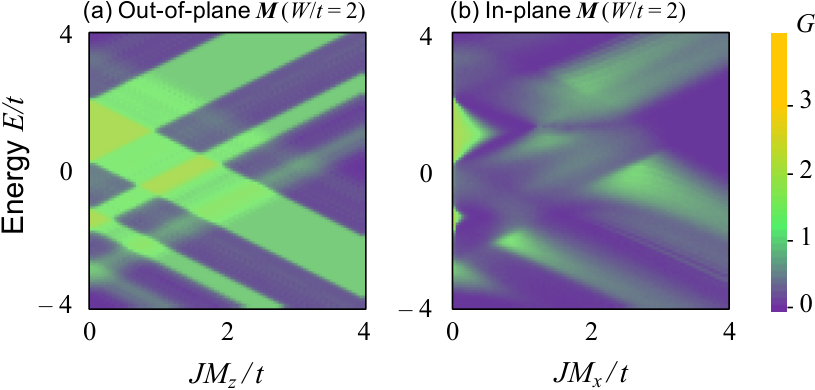
Next we show the magnetization angle dependence of conductance (Fig. 4). For a small , where the magnetization is almost in the out-of-plane direction, the conductance is quantized even in the presence of disorder. This implies that the system is in the QAH state and shows the edge transport. For a large , where the in-plane component of the magnetization becomes large, the system shows conducting or insulating behavior depending on the disorder strength and system size. This is the feature of the diffusive transport. The QAH-diffusive crossover occurs when the bulk band touches the Fermi energy. This crossover is understood as the competition of the spin-orbit term and in-plane component of the magnetization , which opens and narrows the bulk band gap, respectively. This magnetization-angle induced change of transport property leads to an unconventional type of magnetoresistance effect by spatial modulation of the magnetic texture: domain walls.
Domain-wall magnetoresistance. Then we study the transport in systems with domain walls. We consider three types of domain walls: Néel, head-to-head, and in-plane. Note that a Bloch-type wall gives the same results as a Néel type because the in-plane magnetizations, and , are equivalent in our model. The domain walls of thickness can be implemented by position dependent magnetizations,
| (2) |
for a Néel wall,
| (3) |
for a head-to-head wall, and
| (4) |
for an in-plane wall.
Figure 5(a) shows the averaged conductance with uniform magnetizations or domain walls under disorder. The conductance for the out-of-plane uniform magnetization shows that the QAH state (quantized plateau) breaks down around in the case of and . Under the in-plane magnetization (either uniform or domain wall), where the disordered system shows diffusive transport, the conductance quickly decays as the disorder strength increases. On the other hand, the conductance with a Néel or head-to-head domain wall shows an intermediate behavior against disorder.
The DWMR effect is characterized by the magnetoresistance ratio (MR), which is defined by the ratio of the conductance in uniform magnetization to that in a domain wall as
| MR | (5) |
where represents the average over disorder realizations. Figure 5(b) shows the domain-wall MR as functions of disorder strength . The MR for the Néel wall, where and , is significantly large (about ) at a weak disorder. It shows a maximum (about ) at an intermediate disorder strength. The position of the maxima () corresponds to the point where disorder-driven QAH-diffusive crossover occurs. After the transition, the system shows diffusive transport in both the in-plane and out-of-plane magnetizations, and the MR vanishes. This large MR in the Néel wall arises because the diffusive region located around the domain wall works as a resistor in the disorder tolerant QAH states. The MR for the head-to-head wall, where and , becomes negative at a strong disorder, while it is positive and large for a weak disorder. The sign change of the MR occurs when the conductance in the diffusive state becomes comparable with that in the QAH state. Although the MR keeps negative value for a strong disorder, the difference is maximized around the phase transition point . For an in-plane wall, the conductance shows almost the same behavior as the case of uniform magnetization. Thus the MR is vanishing in disordered systems, as in conventional half-metals. In materials with an in-plane easy axis, the in-plane type wall is more favored than the head-to-head type that has the out-of-plane magnetization near the center of the wall, and the huge negative magnetoresistance may be difficult to observe. Therefore, it should be easier to obtain the huge positive magnetoresistance of Néel/Bloch walls in the kagome materials with out-of-plane easy axes, such as thin films of Co3Sn2S2.

Lastly, we study the effect of domain-wall thickness on the MR (see Fig. 6). The magnetoresistance effect in kagome layers with Néel or head-to-head walls is enhanced as the thickness increases. This is in good contrast with a conventional DWMR in half-metals, which quickly vanishes for increasing domain-wall thickness, irrespective of the wall type; the spin of the conduction electron can change gradually and the current can go through the domain walls. At the center of the domain walls, the magnetization is rotated with respect to the background. Therefore the transport properties in both ends (deeply in the domains) and near the center of domain wall are significantly different (diffusive/QAH transport) as shown in Fig. 4; in the presence of disorder, the transport is suppressed in the in-plane magnetized (diffusive) region and enhanced in the out-of-plane magnetized (QAH) region. Therefore the MRs are magnified as the wall (where the transport property changes) thickness increases. We also note that the MR for a thin Néel wall is , because the edge states mix at the domain wall and a half of them go through the wall [see Fig. 6(c)]. The transport in QAH systems with domain-wall resistance is also studied by experiments Yasuda et al. 2017. If there are multiple walls (such as a racetrack memory), the resistance additively increases and the MR becomes huge.

Conclusion. We have studied the transport in disordered ferromagnetic kagome layers. We found a huge and stable DWMR effect originating from the chiral edge states of hte QAH system and the magnetization induced topological phase transition. Considering Néel or Bloch domain walls, we have shown that a huge (around ) MR is achieved, irrespective of the domain-wall thickness and weak disorder strength. We have also shown that a negative DWMR can be realized in the head-to-head wall. These features are contrasted with the conventional DWMR in half-metals, which is always positive, fragile against disorder, and vanishingly small in thick walls. This robust magnetoresistance in QAH kagome layers will make an opportunity to realize the disorder-tolerant and low-power consumption devices. For instance, the current and Joule heating in the racetrack memory can be suppressed by using ferromagnetic kagome layers, such as thin films of Co3Sn2S2. We also note that these topologically protected DWMR effects will pave the way to realize single-material spintronics devices. The absence/presence of a domain wall can be used as “0”/“1”. Furthermore, by simply changing the number of domain walls, we may realize an analog-non-volatile memory, which is now longed for in neuromorphic computing and deep learning. We expect the experimental realization of domain walls in kagome thin-films is not difficult, since the Curie temperature is high enough, K Caer et al. 1978 for Fe3Sn2 and K Liu et al. 2018 for Co3Sn2S2. The domains can be engineered by using a junction of different coercivity or just writing the domains Yasuda et al. 2017.
Acknowledgments. We thank Tomi Ohtsuki, Yuya Ominato, and Mai Kameda for valuable discussions. This work was supported by the Japan Society for the Promotion of Science KAKENHI (Grant Nos. JP15H05854, JP16J01981, JP17K05485, and JP19K14607), and by CREST, Japan Science and Technology Agency (Grant No. JPMJCR18T2).
References
- Parkin et al. (2008) S. S. P. Parkin, M. Hayashi, and L. Thomas, Science 320, 190 (2008).
- Parkin (1995) S. S. P. Parkin, Annu. Rev. Mater. Sci. 25, 357 (1995).
- Haldane (1988) F. D. M. Haldane, Phys. Rev. Lett. 61, 2015 (1988).
- Chang et al. (2013) C.-Z. Chang, J. Zhang, X. Feng, J. Shen, Z. Zhang, M. Guo, K. Li, Y. Ou, P. Wei, L.-L. Wang, Z.-Q. Ji, Y. Feng, S. Ji, X. Chen, J. Jia, X. Dai, Z. Fang, S.-C. Zhang, K. He, Y. Wang, L. Lu, X.-C. Ma, and Q.-K. Xue, Science 340, 167 (2013).
- Wan et al. (2011) X. Wan, A. M. Turner, A. Vishwanath, and S. Y. Savrasov, Phys. Rev. B 83, 205101 (2011).
- Burkov and Balents (2011) A. A. Burkov and L. Balents, Phys. Rev. Lett. 107, 127205 (2011).
- Upadhyaya and Tserkovnyak (2016) P. Upadhyaya and Y. Tserkovnyak, Phys. Rev. B 94, 020411(R) (2016).
- Araki et al. (2016) Y. Araki, A. Yoshida, and K. Nomura, Phys. Rev. B 94, 115312 (2016).
- Kurebayashi and Nomura (2019) D. Kurebayashi and K. Nomura, Sci. Rep. 9, 5365 (2019).
- Kim et al. (2019) S. Kim, D. Kurebayashi, and K. Nomura, J. Phys. Soc. Jpn. 88, 083704 (2019).
- Kent et al. (2001) A. D. Kent, J. Yu, U. Rüdiger, and S. S. P. Parkin, J. Phys.: Condens. Matter 13, R461 (2001).
- Maekawa et al. (2012) S. Maekawa, S. O. Valenzuela, E. Saitoh, and T. Kimura, Spin Current (Semiconductor Science and Technology) (Oxford University Press, Oxford, U.K., 2012).
- Yavorsky et al. (2002) B. Y. Yavorsky, I. Mertig, A. Y. Perlov, A. N. Yaresko, and V. N. Antonov, Phys. Rev. B 66, 174422 (2002).
- Hirschberger et al. (2016) M. Hirschberger, S. Kushwaha, Z. Wang, Q. Gibson, S. Liang, C. A. Belvin, B. A. Bernevig, R. J. Cava, and N. P. Ong, Nat. Mater. 15, 1161 (2016).
- Wang et al. (2016) Z. Wang, M. G. Vergniory, S. Kushwaha, M. Hirschberger, E. V. Chulkov, A. Ernst, N. P. Ong, R. J. Cava, and B. A. Bernevig, Phys. Rev. Lett. 117, 236401 (2016).
- Jin et al. (2017) Y. J. Jin, R. Wang, Z. J. Chen, J. Z. Zhao, Y. J. Zhao, and H. Xu, Phys. Rev. B 96, 201102(R) (2017).
- Ominato et al. (2017) Y. Ominato, K. Kobayashi, and K. Nomura, Phys. Rev. B 95, 085308 (2017).
- Kobayashi et al. (2018) K. Kobayashi, Y. Ominato, and K. Nomura, J. Phys. Soc. Jpn. 87, 073707 (2018).
- Ye et al. (2018) L. Ye, M. Kang, J. Liu, F. von Cube, C. R. Wicker, T. Suzuki, C. Jozwiak, A. Bostwick, R. Rotenberg, D. C. Bell, L. Fu, R. Comin, and J. G. Checkelsky, Nature 555, 638 (2018).
- Yin et al. (2018) J.-X. Yin, S. S. Zhang, H. Li, K. Jiang, G. Chang, B. Zhang, B. Lian, C. Xiang, I. Belopolski, H. Zheng, T. A. Cochran, S.-Y. Xu, G. Bian, K. Liu, T.-R. Chang, H. Lin, Z.-Y. Lu, Z. Wang, S. Jia, W. Wang, and M. Z. Hasan, Nature 562, 91 (2018).
- Liu et al. (2018) E. Liu, Y. Sun, N. Kumar, L. Muechler, A. Sun, L. Jiao, S.-Y. Yang, D. Liu, A. Liang, Q. Xu, J. Kroder, V. Süß, H. Borrmann, C. Shekhar, Z. Wang, C. Xi, W. Wang, W. Schnelle, S. Wirth, Y. Chen, S. T. B. Goennenwein, and C. Felser, Nat. Phys. 14, 1125 (2018).
- (22) L. Muechler, E. Liu, Q. Xu, C. Felser, and Y. Sun, arXiv:1712.08115 .
- Yin et al. (2019) J.-X. Yin, S. S. Zhang, G. Chang, Q. Wang, S. S. Tsirkin, Z. Guguchia, B. Lian, H. Zhou, K. Jiang, I. Belopolski, N. Shumiya, D. Multer, M. Litskevich, T. A. Cochran, H. Lin, Z. Wang, T. Neupert, S. Jia, H. Lei, and M. Z. Hasan, Nat. Phys. 15, 443 (2019).
- (24) A. Ozawa and K. Nomura, arXiv:1904.08148 .
- Liu et al. (2019) D. F. Liu, A. J. Liang, E. K. Liu, Q. N. Xu, Y. W. Li, C. Chen, D. Pei, W. J. Shi, S. K. Mo, P. Dudin, T. Kim, C. Cacho, G. Li, Y. Sun, L. X. Yang, Z. K. Liu, S. S. P. Parkin, C. Felser, and Y. L. Chen, Science 365, 1282 (2019).
- Nakatsuji et al. (2015) S. Nakatsuji, N. Kiyohara, and T. Higo, Nature 527, 212 (2015).
- Yang et al. (2017) H. Yang, Y. Sun, Y. Zhang, W.-J. Shi, S. S. P. Parkin, and B. Yan, New J. Phys. 19, 015008 (2017).
- Ito and Nomura (2017) N. Ito and K. Nomura, J. Phys. Soc. Jpn. 86, 063703 (2017).
- Kane and Mele (2005) C. L. Kane and E. J. Mele, Phys. Rev. Lett. 95, 146802 (2005).
- Guo and Franz (2009) H.-M. Guo and M. Franz, Phys. Rev. B 80, 113102 (2009).
- Caer et al. (1978) G. L. Caer, B. Malaman, and B. Roques, J. Phys. F: Met. Phys. 8, 323 (1978).
- Ando (1991) T. Ando, Phys. Rev. B 44, 8017 (1991).
- Kandala et al. (2015) A. Kandala, A. Richardella, S. Richardella, C.-X. Liu, and N. Samarth, Nat. Commun. 6, 7434 (2015).
- Kou et al. (2015) X. Kou, L. Pan, J. Wan, Y. Fan, E. S. Choi, W.-L. Lee, T. Nie, K. Murata, Q. Shao, S.-C. Zhang, and K. L. Wang, Nat. Commun. 6, 8474 (2015).
- Yasuda et al. (2017) K. Yasuda, M. Mogi, R. Yoshimi, A. Tsukazaki, K. S. Takahashi, M. Kawasaki, F. Kagawa, and Y. Tokura, Science 358, 1311 (2017).