Geometric Scaling of Two-Level-System Loss in Superconducting Resonators
Abstract
We perform an experimental and numerical study of dielectric loss in superconducting microwave resonators at low temperature. Dielectric loss, due to two-level systems, is a limiting factor in several applications, e.g. superconducting qubits, Josephson parametric amplifiers, microwave kinetic-inductance detectors, and superconducting single-photon detectors. Our devices are made of disordered NbN, which, due to magnetic-field penetration, necessitates 3D finite-element simulation of the Maxwell–London equations at microwave frequencies to accurately model the current density and electric field distribution. From the field distribution, we compute the geometric filling factors of the lossy regions in our resonator structures and fit the experimental data to determine the intrinsic loss tangents of its interfaces and dielectrics. We emphasise that the loss caused by a spin-on-glass resist such as hydrogen silsesquioxane (HSQ), used for ultrahigh lithographic resolution relevant to the fabrication of nanowires, and find that, when used, HSQ is the dominant source of loss, with a loss tangent of .
I Introduction


(c) magnitude response of a typical resonator in the single-photon regime (red points). The black line is a fit to determine the resonance parameters.
Several modern circuits rely on superconducting devices with high microwave characteristic impedance and low dissipation. High impedance is usually implemented using the kinetic inductance of a chain of Josephson junctions Masluk et al. 2012; Bell et al. 2012; Manucharyan et al. 2009 or with sub-micron-width wires made of a disordered superconductor such as NbN Niepce et al. 2019, NbTiN Samkharadze et al. 2016, or granular Al Rotzinger et al. 2016; Zhang et al. 2019; Grünhaupt et al. 2019. Despite being less studied, nanowires have some advantages over junction chains— high critical current, magnetic-field tolerance Samkharadze et al. 2016, strong coupling to zero-point fluctuations of the electric field Stockklauser et al. 2017; Samkharadze et al. 2018, less stringent constraints on device geometry, and absence of parasitic modes.
Applications of high-impedance devices include qubit architectures such as the fluxonium Manucharyan et al. 2009; Grünhaupt et al. 2019, which depends on a superinductor (a low-loss inductor with reactive characteristic wave impedance exceeding the resistance quantum, Masluk et al. 2012; Bell et al. 2012; Niepce et al. 2019) and traveling-wave microwave parametric amplifiers Ho Eom et al. 2012; Bockstiegel et al. 2014; O’Brien et al. 2014; White et al. 2015; Macklin et al. 2015; Vissers et al. 2016; Adamyan et al. 2016, relying on the kinetic inductance nonlinearity. Superconducting disordered nanowires are also interesting for newer types of microwave kinetic-inductance photon detectors (MKIDs) Janssen et al. 2012; Schroeder et al. 2019 and radio-frequency-readout of superconducting single-photon detectors (SSPDs) Schroeder et al. 2019; Sinclair et al. 2019.
Dielectric loss and noise associated with two-level systems (TLS) residing in surfaces and interfaces are longstanding problems in superconducting circuits. Specifically, TLS limit the quantum coherence times and lead to parameter fluctuations of superconducting qubits Müller et al. 2015; Klimov et al. 2018; Schlör et al. 2019; Burnett et al. 2019. The participation ratios of the losses of the constituent dielectrics can be estimated through electro-magnetic simulation. Traditionally, the air-facing surfaces are found to be relatively insignificant, instead, the majority of the loss originates from the substrate–metal and substrate–air interfaces Wenner et al. 2011; Wang et al. 2015; Dial et al. 2016; Calusine et al. 2018; Woods et al. 2019. Moreover, for nanowires, the small dimensions exacerbate the TLS contribution to the loss, since the electric field becomes concentrated near the conductor edges. This concentration leads to an increase in the geometric filling factor () of the lossy dielectric layers compared to that of the loss-less vacuum. Therefore, it has been demonstrated that TLS remain the dominant loss mechanism even in disordered superconductors with high kinetic inductance, as long as the films are made moderately thin and not excessively disordered Niepce et al. 2019.
Across nanowire technologies it becomes necessary to use a spin-on-glass resist to define the sub-micron dimensions. The most prevalent spin-on-glass resist is hydrogen silsesquioxane, HSQ. While HSQ offers unmatched resolution ( Chen et al. 2006), its structure after development resembles porous amorphous silicon oxide Namatsu et al. 1998; Liu et al. 1998, which is a well-known host of TLS Barends et al. 2008. HSQ is hard to remove after e-beam exposure, and it is therefore often left on top of the finished devices Niepce et al. 2019.
Therefore, when attempting to understand and improve nanowire device performance, we have a rich landscape of small dimensions, disordered superconductors, and spin-on-glass dielectrics, all three of which are quite different from the more commonly used (and consequently well understood) wide (m) Al or Nb features fabricated with conventional, removable resists.
In this paper, we explore the geometrical scaling, toward nanowire dimensions, of dielectric losses in microwave resonators. We make nominally identical devices with and without spin-on-glass top dielectric and clearly find that in all cases the HSQ makes microwave losses worse. Then, to quantify the loss contributions, we simulate the filling factors and find that due to the ratio of the device dimensions to the London penetration depth, disordered superconductors of small dimensions are not amenable to electrostatic simulations that are traditionally used. To accurately capture the physics, we instead perform 3D finite-element simulations of the current density and electric and magnetic fields at microwave frequencies, from which we extract the various filling factors. This reveals that, while the metal–air interface indeed has a small filling factor, the loss of the HSQ top dielectric is large enough to represent the largest combined loss, in agreement with measurements.
Combining measurements of the loss and numerical simulation of the filling factors of the different interfaces, we determine the value of the loss tangent of HSQ: , i.e. four times that of SiOx O’Connell et al. 2008; Wang et al. 2015; Calusine et al. 2018, which would have been the assumption due to the similarities between spin-on-glass resists and silicon oxide.
II Experimental methods, results


In order to study the geometric scaling of dielectric losses, we fabricated NbN coplanar waveguide resonators, with and without HSQ dielectric on top of the center conductor. These devices spanned a range of widths of the center conductor and of the gap between center conductor and ground planes. The gap width ranges from to , with the ratio of the gap to the centre conductor kept fixed. Figure 1(a) shows a micrograph of a typical device, and Fig. 1(b) shows a sketch of the cross section of the resonators.
The samples are fabricated on a high-resistivity () (100) intrinsic silicon substrate. The substrate is dipped for in a hydrofluoric acid (HF) bath to remove the silicon surface oxide. Within , the wafer is loaded into a UHV sputtering chamber, where a NbN thin-film of thickness is deposited by reactive DC magnetron sputtering from a pure Nb target in a 6:1 Ar:N atmosphere at . Next, a -thick layer of PMMA A6 resist is spin-coated and then exposed by electron-beam lithography (EBL) to define the microwave circuitry and resonators. The pattern is developed for in MIBK:IPA (1:1) and transferred to the film by reactive ion etching (RIE) in a 50:4 Ar:Cl plasma at and . In a subsequent EBL exposure, a layer of HSQ is first spun and then exposed on the center conductor of half of the microwave resonators such that, after development in a TMAH solution, each sample has two copies of each design: one covered with HSQ and one without HSQ.
The samples are wire bonded in a connectorised copper sample box that is mounted onto the mixing chamber of a Bluefors LD250 dilution refrigerator. The inbound microwave signal is attenuated at each temperature stage by a total of before reaching the device under test. Accounting for cable losses and sample-box insertion loss, the total attenuation of the signal reaching the sample is . To avoid any parasitic reflections and noise leakage from amplifiers, the transmitted signal is fed through two microwave circulators (Raditek RADI-4.0-8.0-Cryo-4-77K-1WR) and a 4–8 band pass filter. Finally, the signal is amplified by a LNF LNC4_8A HEMT cryogenic amplifier ( gain) installed on the 2.8-K stage. Additional amplification is performed at room temperature (Pasternack PE-1522 gain-block amplifiers). This measurement environment has been shown to support measurements of resonators with quality factors of several millions Burnett et al. 2018 and therefore provides an ideal test bench for characterising loss in superconducting microwave resonators.
We study the microwave properties of each of these resonators by measuring the forward transmission () response using a Keysight N5249A vector network analyser. When probed with an applied power , the average energy stored in a resonator of characteristic impedance and resonant frequency is given by , where is the average number of photons in the resonator, is Planck’s constant, , and and are the coupling and loaded quality factors, respectively. Figure 1(c) shows a typical magnitude response measured at and has average photon population . The resonator parameters are extracted by fitting the data with an open-source traceable fit routine Probst et al. 2015.
In order to reliably determine the TLS loss contribution, we measure the resonant frequency of each resonator against temperature between and Gao et al. 2008; Lindström et al. 2009 using a Pound frequency-locked loop (P–FLL). The data is shown in Fig. 2, while the cryogenic microwave setup with the VNA and P–FLL schematics are explained in detail in Ref. Niepce et al. 2019. This method only probes TLS effects and has the benefit of being sensitive to a wide frequency distribution of TLS. Consequently, the intrinsic loss tangent is robust against spectrally unstable TLS that produce time variations in the quality factor Earnest et al. 2018. This allows us to independently determine the intrinsic loss tangent (times the filling factor) . The fitted values are presented in Table 1.
| (no HSQ) | (with HSQ) | (no HSQ) | (with HSQ) | ||
|---|---|---|---|---|---|
| () | () | () | () | () | () |
| 5 | 207 | 4027 | 4026 | 1.36 | 1.66 |
| 2 | 312 | 3625 | 3635 | 1.60 | 1.87 |
| 1 | 441 | 4572 | 4626 | 1.98 | 2.50 |
| 0.5 | 632 | 4864 | 4962 | 2.74 | 3.92 |
III Modelling of TLS Loss
Fig. 2 shows that in our devices, the losses are dominated by TLS, even for thin-film nanowires with widths down to 40 nm. In order to accurately account for the individual contributions of all TLS-containing regions of the circuit, we split the dielectric loss into a linear combination of loss tangents each associated with a corresponding filling factor Wenner et al. 2011; Wang et al. 2015; Dial et al. 2016; Gambetta et al. 2017; Calusine et al. 2018,
| (1) |
where is the intrinsic loss tangent of region . Additionally, the filling factor of a given TLS host region , of volume and relative permittivity , is given by
| (2) |
where and are the electric energy stored in region and the total electric energy, respectively, is the electric field, and is the effective permittivity of the entire volume .
Several previous works have studied the loss participation of the different interfaces. O’Connell et al. O’Connell et al. 2008 perform low-temperature, low-power microwave measurements, report the intrinsic loss tangent of dielectrics, and interpret their results using a TLS defect model.
Wenner et al. Wenner et al. 2011 numerically calculate the participation ratios of TLS losses in CPW and microstrip resonators, and find that the losses, at a level of , predominantly arise due to the substrate–metal (SM) and substrate–air (SA) interfaces, with only a 1-% contribution from the metal–air (MA) interface.
Wang et al. Wang et al. 2015 conduct an experimental and numerical study of losses in Al transmon qubits and attribute the dominant loss to surface dielectrics, consistent with the TLS loss model. In a literature study of transmons made with the standard lift-off process, they find a seemingly universal value . We note that the spread between data points pertaining to different devices is within the range of temporal variation, due to spectrally unstable TLS, recently reported in both qubit Burnett et al. 2019 and resonator Earnest et al. 2018.
Dial et al. Dial et al. 2016 experimentally study 3D transmon qubits, with results consistent with the SM and SA interfaces being the dominant contributors to loss.
Calusine et al. Calusine et al. 2018; Woods et al. 2019 trench the substrate of TiN resonators, achieving a mean low-power quality factor of , and demonstrate agreement with a finite-element electrostatic simulation of dielectric loss.
IV Filling Factor Simulations


In order to analyse dielectric and interfacial losses in our devices, and in particular to identify those from the HSQ top dielectric, we perform electro-magnetic simulations (with and without the HSQ layer) in Comsol Multiphysics for a wide range of resonator geometries. A sketch of the cross-section of the simulated structures is shown in Fig. 1(b). The simulation parameters for the constituent materials are as follows: the SA interface is modelled as a thick layer of Morita et al. 1990 with relative permittivity . The MA interface consists of a thick layer of Henry et al. 2017 with relative permittivity Kaiser et al. 2010; Romanenko and Schuster 2017. The SM interface is modelled by a thick layer inside the substrate () Calusine et al. 2018. Finally, the HSQ region has a thickness of and relative permittivity Liu et al. 1998. Because requires several days to achieve any meaningful thickness Henry et al. 2017, it is assumed that no is present underneath the HSQ. Therefore, on the samples without HSQ, resides on both the central conductor and ground planes, whereas on the samples with HSQ, is present only on the ground planes.
The superconductor part of the structure requires extra care to simulate accurately: strongly disordered superconductors, like NbN, have an extremely small electron mean free path (on the order of and smaller Chockalingam et al. 2008) and are therefore in the local dirty limit Dressel 2013. In this limit, several quantities become dependent on the mean free path and need to be adjusted from their BCS values Gor’kov 1959; Tinkham 2004. Most importantly for this study, the magnetic penetration depth in disordered superconductors and at zero temperature becomes
| (3) |
where is the London penetration depth at , is the BCS coherence length, is the reduced Planck constant, is the vacuum permeability, is the superconducting gap at zero temperature, and is the normal-state conductivity. Additionally, the temperature dependence of the penetration depth is given by
| (4) |
By measuring the resistance vs. temperature of our NbN thin films, we find and (measured at the onset of the superconducting transition). Using Mondal et al. 2011, we obtain , which is comparable to the lateral dimension of our resonators.
Consequently, it is not sufficient to approximate the current density in our NbN devices as a surface density, since magnetic fields significantly penetrate the superconductor. This is in contrast to resonators made of a conventional superconductor such as aluminium ( Maloney et al. 1972) or niobium ( Langley et al. 1991). In a similar way, it is insufficient to assume a uniform current distribution in the superconductor when the resonator dimensions are smaller than .
Therefore, a static solution of Maxwell’s equations is insufficient here, in particular for the wider geometries. Instead we need to solve the Maxwell–London equations, at the relevant frequency of the alternating current, in order to accurately simulate the densities of the current and electromagnetic fields. We achieve this in a 3D finite-element simulator by considering the superconductor as an environment with a complex permittivity Vendik et al. 1998; Javadzadeh et al. 2013,
| (5) |
where is the real part of the Mattis–Bardeen conductivity.
The meshing of the simulated structure has to be carefully optimised due the vast difference of length scales within the resonator structure (widths, thicknesses, and also the wavelength). The simulation mesh is manually defined using Comsol’s swept mesh functionality and consists of rectangular elements. Rectangular elements are preferred over the more standard tetrahedral elements to avoid poor meshing quality inherent to high-aspect ratio tetrahedrons. The edge length of each element is varied from to , with smaller elements close to the regions of interest (superconducting thin-film and dielectric layers). Due to memory constraints, however, the edge length alongside the wave propagation direction is kept constant to and only a short section of co-planar waveguide is simulated (). A relative tolerance of was found as a good compromise between the accuracy of the converged solution and the duration of the simulation.
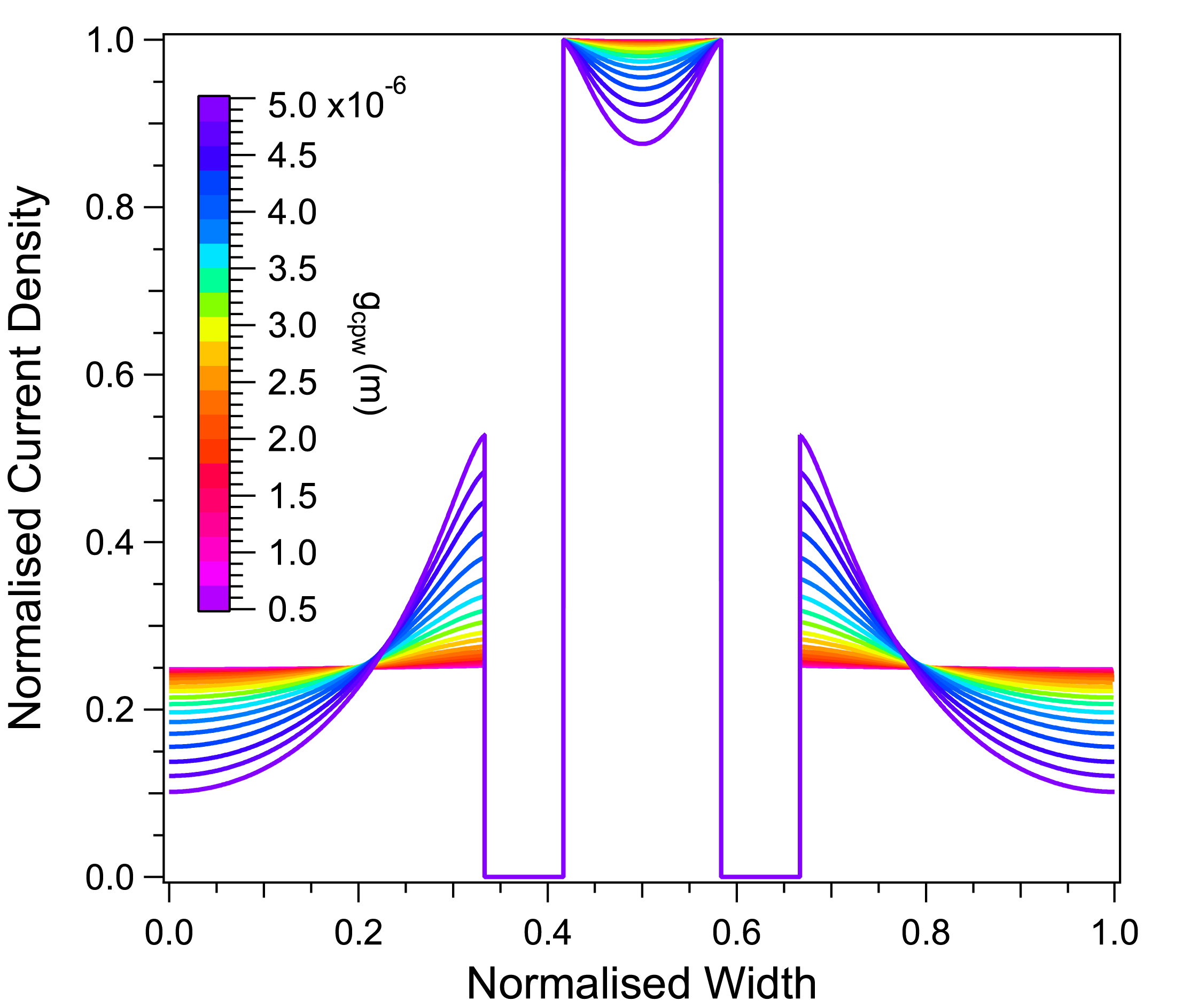
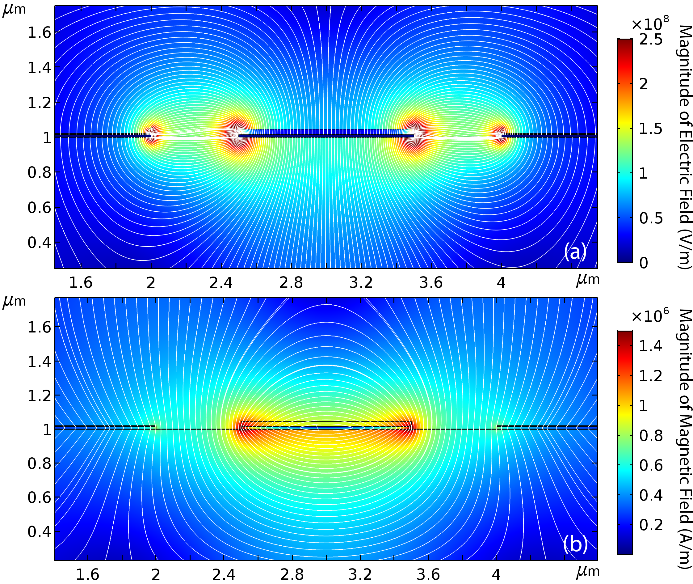
Figures 3–4 show the simulated current density and electric and magnetic fields, respectively, for a cross section of a resonator with . From the electric fields, we calculate the filling factor of each region using Eq. (2) and present the result in Fig. 5. Additionally, Fig. 5 shows filling factors calculated by means of electrostatic simulation to highlight the significant deviation from the Maxwell–London simulation results for .
Using these simulated filling factors, we can fit Eq. (1) to the experimental results in Table 1—see Fig. 6—and in this way determine the intrinsic loss tangent of each lossy region. These results are summarised in Table 2.


| Region | Symbol | Value |
|---|---|---|
| HSQ | ||
| Substrate-Metal Interface | ||
| Niobium Oxide | ||
| Silicon Oxide |
V Discussion
Our results are consistent with values found by other groups in similar types of devices O’Connell et al. 2008; Kaiser et al. 2010; Wang et al. 2015; Calusine et al. 2018. However, we emphasise that the fabrication of our devices was not focused on minimising the influence of TLS.
We find the intrinsic loss tangent for HSQ to be . Paired with the relatively large filling factor of the HSQ region, this makes HSQ the dominant contribution to the loss for all dimensions, as highlighted in Fig. 7; and for a given dimension, is systematically higher for the sample covered with HSQ, as shown in Fig. 6. These results confirms that the porous amorphous silicon oxide structure of developed HSQ Namatsu et al. 1998; Liu et al. 1998 is a major source of dielectric loss, and therefore, a process that allows for the removal of the HSQ mask would lead to significant improvements in device performance.
VI Conclusion
In conclusion, we fabricated and measured co-planar waveguide resonators with dimensions ranging from down to in order to study the geometric dependence of TLS loss. Using 3D finite-element electro-magnetic simulations we calculated the relative contributions of the different sources of TLS loss. Such simulations provide a valuable tool to predict the performance of superconducting resonators and other superconducting quantum devices.
Additionally, by comparing resonators with the central conductor covered by HSQ and resonators without HSQ, we were able to extract the intrinsic loss tangent of this dielectric: .
Acknowledgements.
We acknowledge support in the device fabrication from the Chalmers Nanofabrication Laboratory staff. The authors are grateful to Philippe Tassin for granting access to his nodes in the Chalmers C3SE computational cluster where our simulations were performed. This research has been supported by funding from the Swedish Research Council and Chalmers Area of Advance Nanotechnology. In addition, J.J.B acknowledges financial support from the Industrial Strategy Challenge Fund Metrology Fellowship as part of the UK government’s Department for Business, Energy and Industrial Strategy.References
- Masluk et al. (2012) Nicholas A. Masluk, Ioan M. Pop, Archana Kamal, Zlatko K. Minev, and Michel H. Devoret, “Microwave Characterization of Josephson Junction Arrays: Implementing a Low Loss Superinductance,” Phys. Rev. Lett. 109, 137002 (2012).
- Bell et al. (2012) M. T. Bell, I. A. Sadovskyy, L. B. Ioffe, A. Yu. Kitaev, and M. E. Gershenson, “Quantum Superinductor with Tunable Nonlinearity,” Phys. Rev. Lett. 109, 137003 (2012).
- Manucharyan et al. (2009) Vladimir E. Manucharyan, Jens Koch, Leonid I. Glazman, and Michel H. Devoret, “Fluxonium: Single Cooper-Pair Circuit Free of Charge Offsets,” Science 326, 113–116 (2009).
- Niepce et al. (2019) David Niepce, Jonathan Burnett, and Jonas Bylander, “High Kinetic Inductance NbN Nanowire Superinductors,” Phys. Rev. Appl. 11, 044014 (2019).
- Samkharadze et al. (2016) N. Samkharadze, A. Bruno, P. Scarlino, G. Zheng, D. P. DiVincenzo, L. DiCarlo, and L. M. K. Vandersypen, “High-Kinetic-Inductance Superconducting Nanowire Resonators for Circuit QED in a Magnetic Field,” Phys. Rev. Appl. 5, 044004 (2016).
- Rotzinger et al. (2016) H. Rotzinger, S. T. Skacel, M. Pfirrmann, J. N. Voss, J. Münzberg, S. Probst, P. Bushev, M. P. Weides, A. V. Ustinov, and J. E. Mooij, “Aluminium-oxide wires for superconducting high kinetic inductance circuits,” Supercond. Sci. Technol. 30, 025002 (2016).
- Zhang et al. (2019) Wenyuan Zhang, K. Kalashnikov, Wen-Sen Lu, P. Kamenov, T. DiNapoli, and M. E. Gershenson, “Microresonators Fabricated from High-Kinetic-Inductance Aluminum Films,” Phys. Rev. Appl. 11, 011003 (2019).
- Grünhaupt et al. (2019) Lukas Grünhaupt, Martin Spiecker, Daria Gusenkova, Nataliya Maleeva, Sebastian T. Skacel, Ivan Takmakov, Francesco Valenti, Patrick Winkel, Hannes Rotzinger, Wolfgang Wernsdorfer, Alexey V. Ustinov, and Ioan M. Pop, “Granular aluminium as a superconducting material for high-impedance quantum circuits,” Nat. Mater. , 1 (2019).
- Stockklauser et al. (2017) A. Stockklauser, P. Scarlino, J. V. Koski, S. Gasparinetti, C. K. Andersen, C. Reichl, W. Wegscheider, T. Ihn, K. Ensslin, and A. Wallraff, “Strong Coupling Cavity QED with Gate-Defined Double Quantum Dots Enabled by a High Impedance Resonator,” Phys. Rev. X 7, 011030 (2017).
- Samkharadze et al. (2018) N. Samkharadze, G. Zheng, N. Kalhor, D. Brousse, A. Sammak, U. C. Mendes, A. Blais, G. Scappucci, and L. M. K. Vandersypen, “Strong spin-photon coupling in silicon,” Science 359, 1123–1127 (2018).
- Ho Eom et al. (2012) Byeong Ho Eom, Peter K. Day, Henry G. LeDuc, and Jonas Zmuidzinas, “A wideband, low-noise superconducting amplifier with high dynamic range,” Nat. Phys. 8, 623 (2012).
- Bockstiegel et al. (2014) C. Bockstiegel, J. Gao, M. R. Vissers, M. Sandberg, S. Chaudhuri, A. Sanders, L. R. Vale, K. D. Irwin, and D. P. Pappas, “Development of a Broadband NbTiN Traveling Wave Parametric Amplifier for MKID Readout,” J. Low Temp. Phys. 176, 476–482 (2014).
- O’Brien et al. (2014) Kevin O’Brien, Chris Macklin, Irfan Siddiqi, and Xiang Zhang, “Resonant Phase Matching of Josephson Junction Traveling Wave Parametric Amplifiers,” Phys. Rev. Lett. 113, 157001 (2014).
- White et al. (2015) T. C. White, J. Y. Mutus, I.-C. Hoi, R. Barends, B. Campbell, Yu Chen, Z. Chen, B. Chiaro, A. Dunsworth, E. Jeffrey, J. Kelly, A. Megrant, C. Neill, P. J. J. O’Malley, P. Roushan, D. Sank, A. Vainsencher, J. Wenner, S. Chaudhuri, J. Gao, and John M. Martinis, “Traveling wave parametric amplifier with Josephson junctions using minimal resonator phase matching,” Appl. Phys. Lett. 106, 242601 (2015).
- Macklin et al. (2015) C. Macklin, K. O’Brien, D. Hover, M. E. Schwartz, V. Bolkhovsky, X. Zhang, W. D. Oliver, and I. Siddiqi, “A near–quantum-limited Josephson traveling-wave parametric amplifier,” Science 350, 307–310 (2015).
- Vissers et al. (2016) M. R. Vissers, R. P. Erickson, H.-S. Ku, Leila Vale, Xian Wu, G. C. Hilton, and D. P. Pappas, “Low-noise kinetic inductance traveling-wave amplifier using three-wave mixing,” Appl. Phys. Lett. 108, 012601 (2016).
- Adamyan et al. (2016) A. A. Adamyan, S. E. de Graaf, S. E. Kubatkin, and A. V. Danilov, “Superconducting microwave parametric amplifier based on a quasi-fractal slow propagation line,” J. Appl. Phys. 119, 083901 (2016).
- Janssen et al. (2012) R. M. J. Janssen, A. Endo, J. J. A. Baselmans, P. J. de Visser, R. Barends, and T. M. Klapwijk, “Power Handling and Responsivity of Submicron Wide Superconducting Coplanar Waveguide Resonators,” J. Low Temp. Phys. 167, 354–359 (2012).
- Schroeder et al. (2019) Edward Schroeder, Philip Mauskopf, Hamdi Mani, Sean Bryan, Karl K. Berggren, and Di Zhu, “Operation of a Superconducting Nanowire in Two Detection Modes: KID and SPD,” J. Low Temp. Phys. 194, 386–393 (2019).
- Sinclair et al. (2019) A. K. Sinclair, E. Schroeder, D. Zhu, M. Colangelo, J. Glasby, P. D. Mauskopf, H. Mani, and K. K. Berggren, “Demonstration of Microwave Multiplexed Readout of DC-Biased Superconducting Nanowire Detectors,” IEEE Trans. Appl. Supercond. 29, 1–4 (2019).
- Müller et al. (2015) Clemens Müller, Jürgen Lisenfeld, Alexander Shnirman, and Stefano Poletto, “Interacting two-level defects as sources of fluctuating high-frequency noise in superconducting circuits,” Phys. Rev. B 92, 035442 (2015).
- Klimov et al. (2018) P. V. Klimov, J. Kelly, Z. Chen, M. Neeley, A. Megrant, B. Burkett, R. Barends, K. Arya, B. Chiaro, Yu Chen, A. Dunsworth, A. Fowler, B. Foxen, C. Gidney, M. Giustina, R. Graff, T. Huang, E. Jeffrey, Erik Lucero, J. Y. Mutus, O. Naaman, C. Neill, C. Quintana, P. Roushan, Daniel Sank, A. Vainsencher, J. Wenner, T. C. White, S. Boixo, R. Babbush, V. N. Smelyanskiy, H. Neven, and John M. Martinis, “Fluctuations of Energy-Relaxation Times in Superconducting Qubits,” Phys. Rev. Lett. 121, 090502 (2018).
- Schlör et al. (2019) Steffen Schlör, Jürgen Lisenfeld, Clemens Müller, Alexander Bilmes, Andre Schneider, David P. Pappas, Alexey V. Ustinov, and Martin Weides, “Correlating decoherence in transmon qubits: Low frequency noise by single fluctuators,” arXiv (2019), 1901.05352 .
- Burnett et al. (2019) Jonathan J. Burnett, Andreas Bengtsson, Marco Scigliuzzo, David Niepce, Marina Kudra, Per Delsing, and Jonas Bylander, “Decoherence benchmarking of superconducting qubits,” npj Quantum Inf. 5, 54 (2019).
- Wenner et al. (2011) J. Wenner, R. Barends, R. C. Bialczak, Yu Chen, J. Kelly, Erik Lucero, Matteo Mariantoni, A. Megrant, P. J. J. O’Malley, D. Sank, A. Vainsencher, H. Wang, T. C. White, Y. Yin, J. Zhao, A. N. Cleland, and John M. Martinis, “Surface loss simulations of superconducting coplanar waveguide resonators,” Appl. Phys. Lett. 99, 113513 (2011).
- Wang et al. (2015) C. Wang, C. Axline, Y. Y. Gao, T. Brecht, Y. Chu, L. Frunzio, M. H. Devoret, and R. J. Schoelkopf, “Surface participation and dielectric loss in superconducting qubits,” Appl. Phys. Lett. 107, 162601 (2015).
- Dial et al. (2016) Oliver Dial, Douglas T. McClure, Stefano Poletto, G. A. Keefe, Mary Beth Rothwell, Jay M. Gambetta, David W. Abraham, Jerry M. Chow, and Matthias Steffen, “Bulk and surface loss in superconducting transmon qubits,” Supercond. Sci. Technol. 29, 044001 (2016).
- Calusine et al. (2018) G. Calusine, A. Melville, W. Woods, R. Das, C. Stull, V. Bolkhovsky, D. Braje, D. Hover, D. K. Kim, X. Miloshi, D. Rosenberg, A. Sevi, J. L. Yoder, E. Dauler, and W. D. Oliver, “Analysis and mitigation of interface losses in trenched superconducting coplanar waveguide resonators,” Appl. Phys. Lett. 112, 062601 (2018).
- Woods et al. (2019) W. Woods, G. Calusine, A. Melville, A. Sevi, E. Golden, D. K. Kim, D. Rosenberg, J. L. Yoder, and W. D. Oliver, “Determining Interface Dielectric Losses in Superconducting Coplanar-Waveguide Resonators,” Phys. Rev. Appl. 12, 014012 (2019).
- Chen et al. (2006) Yifang Chen, Haifang Yang, and Zheng Cui, “Effects of developing conditions on the contrast and sensitivity of hydrogen silsesquioxane,” Microelectron. Eng. 83, 1119–1123 (2006).
- Namatsu et al. (1998) H. Namatsu, T. Yamaguchi, M. Nagase, K. Yamazaki, and K. Kurihara, “Nano-patterning of a hydrogen silsesquioxane resist with reduced linewidth fluctuations,” Microelectron. Eng. 41-42, 331–334 (1998).
- Liu et al. (1998) P. T. Liu, T. C. Chang, S. M. Sze, F. M. Pan, Y. J. Mei, W. F. Wu, M. S. Tsai, B. T. Dai, C. Y. Chang, F. Y. Shih, and H. D. Huang, “The effects of plasma treatment for low dielectric constant hydrogen silsesquioxane (HSQ),” Thin Solid Films 332, 345–350 (1998).
- Barends et al. (2008) R. Barends, H. L. Hortensius, T. Zijlstra, J. J. A. Baselmans, S. J. C. Yates, J. R. Gao, and T. M. Klapwijk, “Contribution of dielectrics to frequency and noise of NbTiN superconducting resonators,” Appl. Phys. Lett. 92, 223502 (2008).
- O’Connell et al. (2008) Aaron D. O’Connell, M. Ansmann, R. C. Bialczak, M. Hofheinz, N. Katz, Erik Lucero, C. McKenney, M. Neeley, H. Wang, E. M. Weig, A. N. Cleland, and J. M. Martinis, “Microwave dielectric loss at single photon energies and millikelvin temperatures,” Appl. Phys. Lett. 92, 112903 (2008).
- Gao et al. (2008) Jiansong Gao, Miguel Daal, Anastasios Vayonakis, Shwetank Kumar, Jonas Zmuidzinas, Bernard Sadoulet, Benjamin A. Mazin, Peter K. Day, and Henry G. Leduc, “Experimental evidence for a surface distribution of two-level systems in superconducting lithographed microwave resonators,” Appl. Phys. Lett. 92, 152505 (2008).
- Lindström et al. (2009) T. Lindström, J. E. Healey, M. S. Colclough, C. M. Muirhead, and A. Ya. Tzalenchuk, “Properties of superconducting planar resonators at millikelvin temperatures,” Phys. Rev. B 80, 132501 (2009).
- Burnett et al. (2018) Jonathan Burnett, Andreas Bengtsson, David Niepce, and Jonas Bylander, “Noise and loss of superconducting aluminium resonators at single photon energies,” J. Phys. Conf. Ser. 969, 012131 (2018).
- Probst et al. (2015) S. Probst, F. B. Song, P. A. Bushev, A. V. Ustinov, and M. Weides, “Efficient and robust analysis of complex scattering data under noise in microwave resonators,” Rev. Sci. Instrum. 86, 024706 (2015).
- Earnest et al. (2018) C. T. Earnest, J. H. Béjanin, T. G. McConkey, E. A. Peters, A. Korinek, H. Yuan, and M. Mariantoni, “Substrate surface engineering for high-quality silicon/aluminum superconducting resonators,” Supercond. Sci. Technol. 31, 125013 (2018).
- Gambetta et al. (2017) Jay M. Gambetta, Conal E. Murray, Y.-K.-K. Fung, Douglas T. McClure, Oliver Dial, William Shanks, Jeffrey W. Sleight, and Matthias Steffen, “Investigating Surface Loss Effects in Superconducting Transmon Qubits,” IEEE Trans. Appl. Supercond. 27, 1–5 (2017).
- Morita et al. (1990) M. Morita, T. Ohmi, E. Hasegawa, M. Kawakami, and M. Ohwada, “Growth of native oxide on a silicon surface,” J. Appl. Phys. 68, 1272–1281 (1990).
- Henry et al. (2017) M. David Henry, Steve Wolfley, Travis Young, Todd Monson, Charles J. Pearce, Rupert Lewis, Blythe Clark, Lyle Brunke, and Nancy Missert, “Degradation of Superconducting Nb/NbN Films by Atmospheric Oxidation,” IEEE Trans. Appl. Supercond. 27, 1–5 (2017).
- Kaiser et al. (2010) Ch Kaiser, S. T. Skacel, S. Wünsch, R. Dolata, B. Mackrodt, A. Zorin, and M. Siegel, “Measurement of dielectric losses in amorphous thin films at gigahertz frequencies using superconducting resonators,” Supercond. Sci. Technol. 23, 075008 (2010).
- Romanenko and Schuster (2017) A. Romanenko and D. I. Schuster, “Understanding Quality Factor Degradation in Superconducting Niobium Cavities at Low Microwave Field Amplitudes,” Phys. Rev. Lett. 119, 264801 (2017).
- Chockalingam et al. (2008) S. P. Chockalingam, Madhavi Chand, John Jesudasan, Vikram Tripathi, and Pratap Raychaudhuri, “Superconducting properties and Hall effect of epitaxial NbN thin films,” Phys. Rev. B 77, 214503 (2008).
- Dressel (2013) M. Dressel, “Electrodynamics of Metallic Superconductors,” Adv. Condens. Matter Phys. 2013 (2013), 10.1155/2013/104379.
- Gor’kov (1959) L. P. Gor’kov, “Microscopic derivation of the ginzburg-landau equations in the theory of superconductivity,” JETP 9, 1364 (1959).
- Tinkham (2004) M. Tinkham, Introduction to Superconductivity (Dover Books, 2004).
- Mondal et al. (2011) Mintu Mondal, Anand Kamlapure, Madhavi Chand, Garima Saraswat, Sanjeev Kumar, John Jesudasan, L. Benfatto, Vikram Tripathi, and Pratap Raychaudhuri, “Phase Fluctuations in a Strongly Disordered -Wave NbN Superconductor Close to the Metal-Insulator Transition,” Phys. Rev. Lett. 106, 047001 (2011).
- Maloney et al. (1972) M. David Maloney, Francisco de la Cruz, and Manuel Cardona, “Superconducting Parameters and Size Effects of Aluminum Films and Foils,” Phys. Rev. B 5, 3558–3572 (1972).
- Langley et al. (1991) B. W. Langley, S. M. Anlage, R. F. W. Pease, and M. R. Beasley, “Magnetic penetration depth measurements of superconducting thin films by a microstrip resonator technique,” Rev. Sci. Instrum. 62, 1801–1812 (1991).
- Vendik et al. (1998) O. G. Vendik, I. B. Vendik, and D. I. Kaparkov, “Empirical model of the microwave properties of high-temperature superconductors,” IEEE Trans. Microwave Theory Tech. 46, 469–478 (1998).
- Javadzadeh et al. (2013) S. Mohammad Hassan Javadzadeh, Forouhar Farzaneh, and Mehdi Fardmanesh, “Nonlinear Circuit Model for Discontinuity of Step in Width in Superconducting Microstrip Structures and Its Impact on Nonlinear Effects,” IEEE Trans. Appl. Supercond. 23, 1301208 (2013).