Electron cooling with graphene-insulator-superconductor tunnel junctions and applications to fast bolometry
Abstract
Electronic cooling in hybrid normal metal-insulator-superconductor junctions is a promising technology for the manipulation of thermal loads in solid state nanosystems. One of the main bottlenecks for efficient electronic cooling is the electron-phonon coupling, as it represents a thermal leakage channel to the phonon bath. Graphene is a two-dimensional material that exhibits a weaker electron-phonon coupling compared to standard metals. For this reason, we study the electron cooling in graphene-based systems consisting of a graphene sheet contacted by two insulator/superconductor junctions. We show that, by properly biasing the graphene, its electronic temperature can reach base values lower than those achieved in similar systems based on metallic ultra-thin films. Moreover, the lower electron-phonon coupling is mirrored in a lower heat power pumped into the superconducting leads, thus avoiding their overheating and preserving the cooling mechanisms. Finally, we analyze the possible application of cooled graphene as a bolometric radiation sensor. We study its main figures of merit, i.e., responsivity, noise equivalent power, and response time. In particular, we show that the built-in electron refrigeration allows reaching a responsivity of the order of and a noise equivalent power of order of while the response speed is about corresponding to a thermal bandwidth in the order of .
I Introduction
Low temperature physics at the micro- and nano-scale has found many practical applications in ultrafast electronics for computing Mukhanov 2011; Polonsky et al. 1993; Devoret and Schoelkopf 2013; Wallraff et al. 2004; Vion et al. 2002; Mooij et al. 1999; Fornieri and Giazotto 2017; Paolucci et al. 2018, low-noise high-sensitivity magnetometers Clarke and Braginski 2005; Storm et al. 2017; Giazotto et al. 2010; Ronzani et al. 2014, radiation sensors, and detectors Koppens et al. 2014; Du et al. 2014; Kraus 1996; Lee et al. 2019; Tielrooij et al. 2015; Tielrooij et al. 2017; El Fatimy et al. 2016; Guarcello et al. 2019; Virtanen et al. 2018; Giazotto et al. 2008. Hence, finding novel and efficient cooling schemes is of primary importance Giazotto et al. 2006a; Muhonen et al. 2012. Typically, ultra-low temperature cryogenics is accomplished mainly by exploiting systems consisting of expensive and bulky machines, with unavoidable issues for space or portable applications. For this reason, important efforts are spent in the field of solid state cooling to to realize micro-refrigerators that can be efficient and scalable to an industrial standard. Many different systems have been proposed, based for example on chiral Hall channels Sánchez et al. 2019; Giazotto et al. 2007; Vannucci et al. 2015; Ronetti et al. 2017, adiabatic magnetization Dolcini and Giazotto 2009; Manikandan et al. 2019, piezoelectric elements Steeneken et al. 2011, quantum dots Edwards et al. 1993; Edwards et al. 1995; Hussein et al. 2019, single ions Roßnagel et al. 2016, and engines based on superconducting circuits Karimi and Pekola 2016; Vischi et al. 2019; Virtanen et al. 2017; Marchegiani et al. 2016; Marchegiani et al. 2018.
A cornerstone in this field is the electron refrigeration in voltage-biased Normal metal-Insulator-Superconductor (NIS) tunnel junctions Nahum et al. 1994; Leivo et al. 1996. In such a system, the gap of the superconductor acts as an energy filter for the N metal electrons: under an appropriate voltage bias, only the most energetic electrons, i.e., the hottest ones, are able to tunnel into the superconductor, resulting in a decrease of temperature in the N metal Nahum et al. 1994; Leivo et al. 1996; Muhonen et al. 2012; Giazotto et al. 2006a. The performance of this system is adversely affected by two main phenomena. One consists of an intrinsic thermal leakage owing to the electron-phonon coupling Giazotto et al. 2006a. The phonons of the metal can be considered as a thermal bath, which temperature is set by the substrate temperature. Phonons interact with electrons over the metal volume, consequently supplying heat. Secondly, the heat extracted from the N metal warms up the superconducting leads, with the consequent decrease of the superconducting gap and deterioration of the energy filtering over the electrons Courtois et al. 2016; Nguyen et al. 2013; Hosseinkhani and Catelani 2018.
In this paper, we study the graphene refrigeration based on two Graphene-Insulator-Superconductor (GIS) tunnel junctions forming a SIGIS system. Graphene has several interesting properties compared to metals, for example, a charge carrier concentration-dependent density of states Castro Neto et al. 2009, and a weaker and gate tunable electron-phonon coupling Zihlmann et al. 2019; Chen and Clerk 2012. The weak electron-phonon coupling arises from the graphene dimensionality Borzenets et al. 2013, as tested in other low-dimension materials Karvonen and Maasilta 2007a; Karvonen and Maasilta 2007b. As a consequence, for given cooling power, a SIGIS can reach lower temperatures respect to a SINIS system. Moreover, the lower heat current pumped into the leads decreases their adverse heating, making electron cooling more accessible for concrete applications.
A natural application of electron cooling in SIGIS systems concerns the detection of electromagnetic radiation via bolometric effect. It is known that SINIS systems can be used as bolometers, where the built-in refrigeration enhances the responsivity and decreases the Noise Equivalent Power (NEP) Nahum and Martinis 1993; Nahum et al. 1993; Golubev and Kuzmin 2001; Leonid S. Kuzmin 1998; Schmidt et al. 2005; Lemzyakov et al. 2018. A SIGIS-based bolometer inherits the advantages of built-in refrigeration from a SINIS system, combining them with graphene optoelectronic properties Koppens et al. 2014, such as wide energy absorption spectrum, ultra-fast carrier dynamics Dawlaty et al. 2008; Brida et al. 2013; Xia et al. 2009; Efetov et al. 2018; Mueller et al. 2010, and tunable optical properties via electrostatic doping Li et al. 2008; Wang et al. 2008. In particular, the lower operating temperature and the weaker electron-phonon coupling allow further decreasing the NEP, while the graphene low heat capacity allows a faster response time compared to a SINIS bolometer.
From the industrial point of view, SIGIS systems may also have high potentiality in wafer-scale integration thanks to the high quality currently reached in large-area graphene production Deng et al. 2019. Moreover, the tunnel junction can be realized with hexagonal Boron Nitride (hBN), which is an insulating material extremely suitable to be combined with graphene due to the crystal similarities. Tunnel barriers based on hBN represent a valuable alternative to standard metal oxides insulators, simplifying the fabrication into standard steps. Britnell et al. 2012
The paper is organized as follows. Section II introduces the device model, the GIS tunneling, and the thermal model. Section III studies the graphene base temperature in a biased SIGIS, also giving a comparison with a standard SINIS system. Section IV investigates the system response to perturbations and the related dynamical response time. In section V, we study the bolometric properties by focusing on the responsivity and the NEP. Section VI discusses the impact of the junction quality on the studied properties and yields a quantitative threshold for experiments. Section VII compares our findings with similar bolometric architectures. Finally, section VIII summarizes our main findings.
II Model

We consider the system sketched in Fig. 1. It consists of a graphene sheet contacted by two superconducting leads through tunnel junctions of resistance each. Superconductors are assumed made of aluminum with superconducting gap and critical temperature . The graphene can be deposited directly on or hBN. The graphene sheet has a rectangular area, with geometrical dimensions . The two leads, with dimensions , are placed at distance (see Fig. 1b) and connected to a voltage generator . The electric current is determined by and the graphene sheet resistance , where the sheet resistivity depends on the carrier density and the electron mobility , being the modulus of the electron charge. The graphene is gated with a back-gate placed under the substrate and connected to an external generator .
The proposed setup has many geometrical/fabrication parameters. As a consequence, we fix some of them to reasonable experimental values. By choosing proper geometrical dimensions for the graphene sheet, we consider a negligible sheet resistance compared to the tunnel resistance (). This assumption allows neglecting the voltage partition between the junctions and the sheet. So, the Joule heating of graphene results negligible. To this aim, we set the aspect ratio to , corresponding to for graphene with and residual carrier density , typical for graphene on Chen et al. 2008; Martin et al. 2007; Das Sarma et al. 2011. A similar value of resistance can be considered for an encapsulated graphene in a hBN/G/hBN heterostructure, where mobilities are commonly over but the residual charge densities are lower than Amet et al. 2014; Amet et al. 2015; Mayorov et al. 2012; Banszerus et al. 2015. An advantage of the encapsulated graphene is that the top layer of ultra-thin hBN can be exploited as a high-quality tunnel junction Britnell et al. 2012.
We consider a large graphene area . Large area samples are preferred for bolometric applications since they keep the device in linear response regime and extend the dynamical range of the detector McKitterick et al. 2015; Du et al. 2014. Moreover, a greater area reduces the temperature fluctuations, since the thermal inertia due to the heat capacity scales with the area.
Finally, we fix the tunnel resistance as . This value is compatible with tunnel junction made of 2-layer hBN Britnell et al. 2012; Zihlmann et al. 2019 and makes the assumption valid. We also observe that the tunnel barriers suppress the superconducting proximity effect in graphene.
Table 1 is a summary of the parameters adopted in the numerical simulations. Some of them will be introduced in the following.
| Graphene dimensions | |
|---|---|
| Graphene area | |
| Residual electron density | |
| Tunnel resistance | |
| Sheet resistance | |
| Electron-phonon coupling | (dirty case) |
| (clean case) | |
| Heat capacity at |
II.1 GIS tunneling and cooling
Here, we introduce the main equations and discuss the electron tunneling through a GIS junction. The tunneling rate is proportional to the Density of States (DoS) of graphene and superconductor Maiti et al. 2012. The graphene DoS reads Castro Neto et al. 2009
| (1) |
where is the energy, is the DoS at the Fermi level, is the normalized graphene DoS and is the Fermi energy. The DoS at the Fermi level is related to the carrier density by and where m/s is the Fermi velocity Castro Neto et al. 2009 and is the reduced Planck constant.
The superconductor DoS is
| (2) | ||||
| (3) |
where is the energy, is the DoS at Fermi level of the normal state aluminum, is the superconductor normalized DoS, is the temperature-dependent superconductivity gap of the Bardeen-Cooper-Schrieffer (BCS) theory and is the Dynes parameter that phenomenologically takes into account the subgap tunneling and the smearing of the superconducting peaks, which are also related to the quality of the junction. In this paper, we fixed , for simplicity. In section VI, we show the dependence of the results on higher values of .
The charge current in a GIS tunnel junction can be expressed as Maiti et al. 2012; Zihlmann et al. 2019
| (4) |
where is the voltage drop across the tunnel junction, and are the graphene and superconductor electronic temperatures, respectively. Finally, is the Fermi distribution. In the following we assume that .
Similarly, the heat current from G to S is
| (5) |
We set the sign convention such that means that the heat is extracted from graphene towards superconductors. It is important to note that when the graphene Fermi energy is much greater than the superconducting gap , the graphene DoS dependence on energy can be disregarded in the tunneling integrals, i.e., . Indeed, for , the distribution defines an energy bandwidth of a few around the Fermi level. In this energy window, the graphene DoS has a variation of the order of that can be hence neglected when . This condition, in general, holds experimentally, as indicated by the presence of a residual charge density Mayorov et al. 2012. The lowest values of residual charge density can be obtained in high quality hBN/G/hBN heterostructures and unlikely goes below Arjmandi-Tash et al. 2018; this value corresponds to the lowest value of Fermi energy , that is at least 100 times the value of , confirming . We remark that the BCS theory provides that , implying that , i.e., ensuring that the superconducting gap is lower than the Fermi energy at every temperature.
Therefore, tunneling integrals in Eqs. (4), (5) take the standard functional form of the NIS tunneling expressions Muhonen et al. 2012; Giazotto et al. 2006a; Anghel and Pekola 2001; Müller and Chao 1997. We point out that this approximation does not completely drop out the dependence of the tunnel integrals on the Fermi level/carrier density. It is indeed still contained in . We will discuss this point better at the end of this subsection.

Figure 2a displays the behavior of versus and is equal to the bath temperature . In the regions where , the heat is extracted from graphene, implying electron cooling. It corresponds to the yellow-green area delimited by the white curve (). The cooling power is maximized, for given value of , at the optimal voltage bias (see red curve in Fig. 2a). The cooling power value along the curve is reported in Fig. 2b as function of . The maximum is about for K and ( for aluminum). For , the maximum cooling power corresponds to about .
Low temperature () approximated expressions of Eqs. (4) and (5) are reported in Refs. Giazotto et al. 2006a; Muhonen et al. 2012; Anghel and Pekola 2001; Müller and Chao 1997. In this approximation, the optimal cooling is (see the dotted black curve in Fig. 2a), corresponding to an electric current
| (6) |
and a related cooling power
| (7) |
Before concluding this section, we wish to discuss the dependence of equations (4) and (5) on the carrier density and how this can affect the electronic and thermal transport. The carrier density is tuned via field effect by the gate voltage (see Fig. 1a). The electric and thermal currents depend on through the tunnel resistance . The latter is proportional to the DoS of both graphene and superconductor and to the modulus square of the tunneling amplitude , i.e. Maiti et al. 2012; Heikkilä 2013. Since , the GIS tunnel resistance depends on the carrier density as
| (8) |
where is the residual carrier density. This equation implies
| (9) | ||||
| (10) |
This simple scaling on is valid when the approximation , i.e. when . This condition is experimentally respected since charge density can be tuned typically in a range from to , when using standard solid gating. This range is experimentally limited on the bottom by the presence of charge puddles Martin et al. 2007 and on the top by the occurrence of gate dielectric breakdown caused by high voltage.
II.2 SIGIS Thermal model
In this section, we describe the thermal model that includes all the thermal channels to graphene, as sketched in Fig. 2c. We consider the graphene sheet homogeneously at the same temperature, neglecting the spatial dependence of , thanks to the high heat diffusivity in graphene Dawlaty et al. 2008; Brida et al. 2013; Xia et al. 2009. Moreover, we treat the graphene phonon bath as a reservoir at a fixed temperature . This assumption is physically reasonable owing to the negligible Kapitza thermal resistance between the graphene and the substrate Balandin 2011; Chen et al. 2009. Finally, we consider the superconductor electrons as a thermal reservoir well thermalized with the substrate, by imposing . This assumption can be violated in real experiments, where the heat pumped into the superconductor heats up its quasi-particles, and the weak electron/phonon (e/ph) coupling provides a poor cooling to the bath Giazotto et al. 2006a. This effect is detrimental for the superconducting state and, as a consequence, for cooling. In general, this effect can be weakened by contacting the superconductor with hot quasi-particles traps or coolers in cascade Courtois et al. 2016; Nguyen et al. 2013; Hosseinkhani and Catelani 2018; Nguyen et al. 2016; Camarasa-Gómez et al. 2014, making our assumption physically reasonable. Moreover, in a SIGIS system, the amount of heat transferred into the superconductor is lower than that present in a SINIS system, because of the lower heat leakage from the phonon bath to the graphene electrons.
Thus, in our thermal model (see Fig. 2c) the only variable is the graphene temperature , which is determined by the solution of the following heat balance equation
| (11) |
This equation takes into account the heat current across the two junctions , the electron-phonon coupling in graphene , the Joule heating and a possible external power input (for example a radiation power) that we consider to investigate the bolometric response. We also consider the time dependence of introducing the electron heat capacity , which plays the role of thermal inertia of the system when dynamic response is investigated.
Let us consider the electron-phonon heat current . Below the Bloch-Grüneisen temperature (), is characterized by the presence of two different regimes depending on whether the wavelength of thermal phonons is longer or shorter than the electron mean free path Zihlmann et al. 2019; Chen and Clerk 2012; Efetov and Kim 2010; Hwang and Das Sarma 2008; Gonnelli et al. 2015. In the clean regime (or short wavelength regime) the e/ph coupling reads
| (12) | ||||
| (13) |
while in the dirty regime (or long wavelength regime) takes the form
| (14) | ||||
| (15) |
where , are the electron-phonon coupling constants, depending on the sound speed , the mass density , the deformation potential , and the Riemann Zeta . As final result, the coupling constants are and Walsh et al. 2017; Zihlmann et al. 2019; Chen and Clerk 2012; Viljas and Heikkilä 2010; Castro Neto et al. 2009; McKitterick et al. 2015; Paolucci et al. 2017.
In the following we consider both the graphene regimes, writing the generic coupling , where can be 3 or 4 according to a dirty or clean regime respectively and is or coherently. In the temperature range between to , graphene on shows a dirty regime, while the hBN-encapsulated graphene is in a clean regime McKitterick et al. 2015; Zihlmann et al. 2019. The reason is the different mobility (and therefore different electron mean free path) due to the presence of the hBN-encapsulation Chen and Clerk 2012; McKitterick et al. 2015; Zihlmann et al. 2019.
The effect of the two regimes can be evaluated by the electron-phonon thermal conductance in a system where is perturbed from the equilibrium. is calculated by the linear expansion where
| (16) |
The in the two regimes are of the same order of magnitude at K, but the different temperature scaling makes the clean regime weaker compared to the dirty one when is below .
The Joule heating is due to the electron current flow in the resistive sheet of graphene. It is given by and is a component that spoils cooling. In this system, the current-voltage characteristic is non-linear, and the current is suppressed by the presence of the superconductor gap. The Joule heating scales as , while the cooling power as . The ratio between the Joule heating and the cooling power then scales as , implying that the cooling performance is not affected by the Joule effect when . Indeed, we found out in our simulations that Joule heating weakly affects the thermal equilibrium, which is instead dominated by the competition between , , and . For this reason, we neglect the Joule heating in the analytic results, while we keep it in the numerical ones.
We remark that, in our thermal model, we do not include the photonic and the phenomenological back-tunneling channels Walsh et al. 2017; Schmidt et al. 2004; Meschke et al. 2006; Muhonen et al. 2012; Jochum et al. 1998. These two contributions are indeed dependent on the fabrication parameters, such as the device design and on the junction quality. For this reason, they are often considered as empirical parameters to fit the experimental data. Moreover, in the range of temperatures studied in this paper (above 0.1 K), the photonic thermal conductance in our device is negligible compared to the phononic thermal conductance Walsh et al. 2017. Finally, the quasi-particle back-scattering can be managed by adjusting the tunnel resistance of the junction.
The heat capacity for is given by the standard Fermi liquid result Falkovsky 2013; Viljas and Heikkilä 2010; Walsh et al. 2017
| (17) |
where is the Sommerfeld coefficient. We notice that the linear behavior of in temperature owes to the fact that , yielding the same behavior of a metal. The dependence of on the Fermi energy (and hence by the residual charge by ) is contained in .
Finally, we comment on the dependence of the heat current contributions on carrier density. For simplicity, we assume a homogeneous charge density over the whole graphene area, even though under the metallic contacts the screening may slightly affect this assumption. Anyway, since cooling require very small potential differences (mV) between the contacts and graphene, the electron density under the electrodes can be considered constant. Hence, the carrier density of the whole graphene sheet can be tuned mainly by the backgate, with negligible charge inhomogeneities due to the specific electrostatic problem. We recall that the sheet resistivity is given by , implying
| (18) |
This equation and in Eq. (8) return that does not depend on . Moreover, considering Eq. (10) and , the heat balance equation can be written as
| (19) |
The dominant terms and scale as . The terms that are constant in are the Joule heating and the external power input . Hence, the thermal properties are weakly affected by the graphene carrier density if Joule heating is negligible and . The heat balance equation in presence of an external source () will be discussed in section V.
III Base temperature

In this section, we investigate the stationary () quasi-equilibrium case of the heat balance equation (11) in the absence of external input power (). Solving the balance equation for , we can calculate the base temperature reached by cooled graphene.
Fig. 3a reports a color map of versus for the case of clean graphene regime. The black line for separates the region of cooling and heating of graphene. Figure 3b reports versus for chosen values of bath temperature . When , the graphene temperature tends to the equilibrium with the bath temperature . The minimum temperature is reached when the voltage bias is set closely below . In the dirty regime, the cooling behavior is qualitatively similar but lower in performance compared to that in the clean graphene regime, due to the stronger e/ph thermal conductance (see Eq. (16)), implying higher base temperatures.
When Joule effect is negligible, the base temperature is given by the equilibrium between the electron-phonon heating power and the junction cooling power. The former scales as the area , while the latter scales as . As a consequence, the base temperature is lowered by decreasing the factor . The junction resistance cannot be decreased at will since the condition must be satisfied; otherwise, the detrimental Joule heating contribution is not negligible, and the voltage partition between sheet and junctions must be properly considered.
The heat balance equation can be solved analytically at optimal bias and low temperatures if the Joule heating is negligible and if the graphene is in the dirty regime. With these assumptions, Eq. (7) can be used for and then the heat balance equation has a polynomial form that can be solved exactly. On the opposite, the form of the e/ph coupling in clean regime yields a not analytically solvable balance equation. The analytic solution is obtained by substituting with the Eq. (7) and with Eq. (15) in the thermal balance equation , yielding
| (20) |
that is a second-order equation in and
with physical solution
| (21) |
Fig. 3c reports the dependence of on calculated numerically in case of dirty and clean regimes. The analytical result of Eq. (21) for in the dirty regime is represented by the red dashed line. We can notice that decreasing further reduces the achievable base temperature. The agreement between the numeric and analytic results for in the dirty regime is generally good if . When , the solution depends on the accuracy of the approximation with the consequence that the leading order approximation of in Eq. (7) is not anymore sufficient.
In order to investigate the advantage of graphene e/ph coupling, we make a comparison of the base graphene temperature in a SIGIS with the base temperature of a tunnel-cooled system based on a metallic thin film and a two-dimensional electron gas (2DEG). To this aim, we solve the balance equation for the different systems, where is the same but is the electron-phonon heat current in a metallic thin film or in a conventional 2DEG with parabolic band dispersion Giazotto et al. 2006b. For simplicity, we neglect the resistances of metal and 2DEG and the related Joule heating. For the sake of comparison, we consider the same and . For a metallic thin film, it is and , where is the electron temperature. We consider a low thickness nm, for which we have a coupling per unit area . For a 2DEG in , we have and a coupling per unit area Giazotto et al. 2006b; Price 1982; Ma et al. 1991. At a temperature of the order of 1K, the coupling per unit area of the metal is about 40 times larger than that of graphene, while the coupling per unit area of the 2DEG is about 3 times larger. It can be expected that graphene and 2DEG can reach lower temperatures compared to the metallic thin film. This is shown in Fig. 3d, reporting the base temperatures of the different systems.
Deeper insight can be reached by comparing the e/ph thermal conductance per unit area of the different systems. We have in a metal , in a 2DEG and in graphene , with indicating different e/ph regime. It can be noticed that the former two have a better scaling behavior compared to graphene. However, in metals, the coupling constant is large enough that this advantage is effective only below K, i.e., below the typical temperature range for the tunnel cooling. This can be seen in Fig. 3d where the metal curve reaches the graphene curves (dirty and clean) at about . We remark that a thick metallic film is very challenging to be produced. A different conclusion holds for the 2DEG where the coupling constant is low enough that the scaling of can allow for a lower e/ph heat current in the temperature interval of interest. This can be seen in Fig. 3d, where the 2DEG reaches the base temperature of graphene at K for dirty regime and at K for clean regime. This indicates that cooling performances for a 2DEG and a SIGIS are comparable. In this case, the main (and non-trivial) advantage in graphene relies on the fabrication issues. Indeed, the growth of III-IV materials for 2DEGs requires molecular beam epitaxy that is an expensive technique. Furthermore, the use of 2DEGs implies the use of several steps of lithography, etching, and evaporation of metals. On the opposite, Chemical Vapor Deposition is nowadays an established and cheaper technique for growing graphene or hBN/graphene/hBN heterostructures Banszerus et al. 2015, allowing easier scalability to industrial standards.
IV Thermal Response Dynamics
In this section, we study the dynamics of the SIGIS with thermal perturbations from the base temperature, focusing on its response time. The latter is an important parameter for any time-dependent application since it affects the thermal bandwidth of the system.
The response time is a parameter that appears in the transfer functions and involves thermal properties, such as the power-to-temperature transfer function or the bolometric responsivity. Both these quantities are studied below.
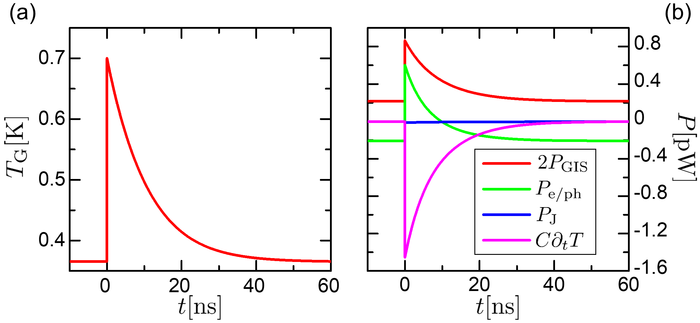
As an example of thermal response, we report in Fig. 4 the numerical solution of the heat balance equation (11) at bath temperature K, optimal voltage bias and dirty graphene regime. Figure 4a shows the evolution of temperature over time. At , the graphene is at base temperature K. The input power is null for the whole process, except at , where a power pulse drives the graphene temperature from to K. After this pulse, the graphene thermalizes to the bath temperature in about 50 ns. The associated heat currents evolution is plotted in Fig. 4b. In the whole process, it is . At , the graphene is in a stationary state, where and the equilibrium is given by . From Fig. 4b it can be noticed that the numerical calculations yield an always negligible Joule heating.
Important physical insight into the dynamics can be obtained by studying small perturbations from base temperature by linearizing the heat balance equation. Therefore, we consider the left hand side of Eq. (11) in a series expansion around and we assume a constant heat capacity for small perturbations: . Moreover, we neglect Joule heating. In this way, we have the linearized thermal equation
| (22) |
where , and and are thermal conductances related to the junction and the e/ph coupling, respectively. The first term is
| (23) |
where the approximation in the last passage is valid at and . The e/ph channel is given by Eq. (16) evaluated at the equilibrium point .
The solutions of the linearized thermal balance equation (22) have the exponential form , where is the response time at given by
| (24) |
The denominator in Eq. (24) is the sum of the junction and e/ph thermal conductances. The different temperature scaling of and implies two regimes defined by the dominance of one of the two channels. The two regimes are separated by a crossover temperature that can be estimated by equation , yielding:
| (25) |
We obtain K for dirty graphene regime and K for clean graphene regime. When the junction conductance dominates over the e/ph conductance and is
| (26) |
For , there is a regime dominated by the e/ph coupling, yielding
| (27) |
that depends only on the graphene properties and not on geometrical parameters of the SIGIS.

Figure 5a shows the dependence of on at optimal voltage bias for different values of . The solid lines correspond to Eq. (24) where is given by Eq. (21). The dashed lines are obtained by numerically solving the heat balance equation when perturbing the graphene base temperature of 10%. The numerical and analytical results are in good agreement. The maximum of each curve is the crossover point between the two regimes dominated by the junction [Eq. (26)] and the e/ph coupling [Eq. (27)]. The response time increases with , since the thermal conductance of the junction is lowered. In particular, at low , the curves of Fig. 5a indicate that as given by Eq. (26).
The results in Eq. (24) and Fig. 5a are obtained for . has a dependence also on the bias voltage, since the latter tunes the transport properties of the junction. Figure 5b reports versus calculated for different bath temperatures in the case of dirty graphene regime. We notice that the response time decreases from at to at when K, because when the cooling operates, the junction thermal conductance is enhanced.
This point can be investigated analytically. To evaluate the voltage dependence of the thermal response at small bias, we need the thermal conductance of the junction . It can be approximated by the tunnel integral expression in Eq. (23) at . At the leading order we obtain finally
| (28) |
Linearizing the heat balance equation around the equilibrium state we obtain
| (29) |
The difference between [Eq. (28)] and [Eq. (23)] is strong. In particular, at low temperatures the junction conductance is exponentially suppressed at zero bias, while has a large contribution in the optimally biased case.
The difference of between the biased and unbiased case is remarked in Fig. 5c. Dashed curves show in an unbiased system at , while solid curves show for and are set subsequently. For completeness, we show both the dirty (blue curves) and clean (red curves) graphene regimes. The difference in response time between and can reach one or two orders of magnitude depending on the value of and the graphene regime. Furthermore, at , there is no maximum in , since both the and are increasing functions of .
It is worth to note that the response time does not depend on carrier density . Indeed, both and are proportional to . As a consequence, the gating does not affect .
Finally, we evaluate the temperature response to a finite external power signal . This quantity will be exploited for investigating the bolometric response of the device. It is useful to write the linear heat balance equation (22) in the frequency domain including the signal . We remark that the frequency of refers to the Fourier component of the power and not to the electromagnetic frequency. The resulting equation takes the form
| (30) |
where is the power-to-temperature transfer function. This equation shows that the SIGIS responds as a low-pass filter with cut-off frequency . Considering the values of reported in Fig. 5a, the corresponding frequency is in a range of . In the following section, this transfer function will be used to evaluate the responsivity, a figure of merit which quantifies the SIGIS performances as a bolometer.
V Biased SIGIS as a bolometer
In this section, we study the cooled SIGIS as a bolometer. An input power is converted in a variation of current when the SIGIS is kept at a constant voltage bias. In detail, we characterize two bolometric figures of merit, the responsivity and the NEP.
The bolometric properties of a SINIS system with electron cooling have been studied in literature Golubev and Kuzmin 2001; Leonid S. Kuzmin 1998; Lemzyakov et al. 2018; Kuzmin et al. 2019. The main result is that the built-in refrigeration enhances the responsivity and decreases the NEP. Here, we essentially follow a similar analysis for a SIGIS.
We point out that SIGIS systems have already been investigated in literature, at , where the cooling is negligible Vora et al. 2012; McKitterick et al. 2015; Du et al. 2014. The purpose of these low schemes is to decrease the thermal conductance across the junction in order to use the device at lower input power regimes Vora et al. 2012; McKitterick et al. 2015; Du et al. 2014.

Our bolometer scheme consists of a SIGIS system connected to an external voltage generator , being the voltage drop across a single junction (see sketch in Fig. 6a). The graphene is also connected to the superconducting antenna by means of a clean superconductor/graphene junction. The superconducting antenna allows carrying the power and traps it in graphene since the superconducting leads work as Andreev mirrors Golubev and Kuzmin 2001; Nahum and Martinis 1993, reducing the thermal leakage to the antenna. It is important to remark that the distance between the antenna electrodes must be enough to make the Josephson coupling through proximity effect negligible Heersche et al. 2007. The electric current in the circuit is measured by means of an inductance coupled to a superconducting interferometer read-out Clarke and Braginski 2005; Giazotto et al. 2010; Giazotto and Taddei 2011; Ronzani et al. 2014; D’Ambrosio et al. 2015.
V.1 Responsivity
We start our investigation with the responsivity, defined as a power-to-current transfer function:
| (31) |
where and are the electric current and the input power signal in the frequency domain, respectively.
We calculate the responsivity as the product of the power-to-temperature transfer function in Eq. (30) with the temperature-to-current transfer function . The product of the two transfer functions is equivalent to calculate the derivative by the factorization , since Golubev and Kuzmin 2001. We obtain
| (32) |
The responsivity has a cut-off at the frequency .
We focus on the low frequency limit, which is valid when the band of the input signal is sufficiently below the cut-off frequency. Fig. 6b reports a color map of versus and , obtained by Eq. (32) using the numerical derivative of Eqs. (4), (5). Cuts of Fig. 6b versus are reported in Fig. 6c. The responsivity shows a peak on the red dashed curve . The latter does not coincide with (dotted black in Fig. 6b), which maximizes the cooling performances. Indeed, and are different by definition, since the former is obtained by maximizing and the latter by maximizing . is located closely below . Above this voltage, the current characteristics lose sensitivity to temperature since they converge to the ohmic behavior . On the other hand, for well below the gap, the current is suppressed.
Other physical features of responsivity are represented in Fig. 6d. Here, the solid curves are calculated by considering the graphene cooling, while the dashed curves are obtained by imposing , i.e., disregarding the cooling effect. This treatment corresponds to a physical situation where a spurious heating source completely spoils the cooling power of the junction. Let us investigate how the difference of graphene regime affects the responsivity. We first consider the dashed curves in Fig. 6d, representing the absence of cooling, where we can notice that the clean case is slightly more responsive. The reason is due to the enhanced power-to-temperature transfer function . Indeed, in both the dashed results (), the temperature to current transfer function in Eq. (32) is the same, since it is a property of the junction depending only on , and . But the transfer function changes between a clean or dirty graphene regime, since the phonon thermal conductance is lower in the clean case. This means that, given a power input, the temperature raise is bigger in the clean case, resulting in a greater current response.
The comparison between the dashed and solid curves in Fig. 6d shows that the presence of an active cooling enhances the responsivity. The graphene base temperature is lower for clean graphene regime (see Sec. III), resulting in a stronger enhancement of responsivity compared to the dirty graphene case.
A physical insight to this argument can be obtained by using the low temperature approximations studied above. We underline that these expressions hold for and not , but they give enough information for a physical picture. The responsivity at low temperatures is
| (33) |
As in the previous section, the denominator shows the presence of two regimes separated by the crossover temperature in Eq. (25). The regime at is dominated by the e/ph thermal channel with responsivity
| (34) |
The regime at is dominated by the junction thermal channel with responsivity at
| (35) |
This expression does not involve any graphene property, but it is obtained by the ratio of the two junction properties and . In particular, both terms scale as , so the tunnel resistance does not directly affect the responsivity at low temperatures.
Finally, we would like to stress that the responsivity increases by decreasing the graphene temperature. This is also confirmed by Fig. 6b,c.
V.2 Noise equivalent power

We now focus on the noise equivalent power, which is defined as the signal power necessary to have a signal-to-noise ratio equal to 1 with a bandwidth of 1 Hz Richards 1994.
The total NEP of the SIGIS is given by different contributions Golubev and Kuzmin 2001
| (36) |
where the three terms are related to the junction, the e/ph coupling and the amplifier read-out, respectively. The factor 2 in front of takes into account the two junctions, assuming their noises to be uncorrelated Giazotto and Pekola 2005, which is related to the fact that temperature fluctuations, as the one induced by heat noise, are small in comparison to the stationary value of Guarcello et al. 2019.
The contribution to the junction NEP is given by fluctuations in both the electric and heat currents:
| (37) |
where the quantities in angled brackets are the low frequency spectral densities of fluctuations Golubev and Kuzmin 2001. is the current fluctuation given by Golubev and Kuzmin 2001
| (38) |
The fluctuation of the tunneling rate is mirrored in a fluctuation of the tunneled heat
| (39) |
Since the two fluctuations and are given by the tunneling of the same carriers, a non-null correlation exists Golubev and Kuzmin 2001:
| (40) |
In these integrals, the energy dependence of graphene has been neglected, according to the approximation done in Sec. II.
Figure 7 reports the NEP components for K. Panel (a) shows the contributions to in Eq. (37). For completeness, the NEP calculated by neglecting the cross-correlation between and is also reported
| (41) |
By comparing and we can notice that the term brings a correction that reduces the total NEP. The cross-correlation is positive except in the region above the gap voltage . Outside this region, the cross-correlation partially cancels the shot noise and the heat noise Golubev and Kuzmin 2001.
The NEP due to the junction noise is smaller in a SIGIS bolometer compared to a SINIS bolometer. Indeed, scales as and good cooling characteristics can be reached in a SIGIS with a tunnel resistance one order of magnitude greater compared to a SINIS. As a consequence, the is lower of a factor .
Let us consider the other NEP contributions. The contribution related to the noise in the e/ph channel can be roughly estimated by a generalization of expression in Ref. Golubev and Kuzmin 2001
| (42) |
At equilibrium , the NEP takes the standard form McKitterick et al. 2015; Du et al. 2014. We notice that this term is smaller in a SIGIS compared to a SINIS, due to the lower e/ph coupling constant (see discussion in Sec. III). In the temperature range of 0.1K-1K, the e/ph thermal conductance is one order of magnitude lower, yielding a decrease of a factor .
Finally, we consider the read-out NEP due to the amplifier noise
| (43) |
and we assume Golubev and Kuzmin 2001.
Panel (b) of Fig. 7 shows the different contributions to the total NEP at K versus . Panels (a) and (b) show the same . We notice that has a minimum close to the optimal bias. Here, the three contributions are of the same order of magnitude and yield . Away from the optimal point, the read-out dominates. Hence, in order to optimize the total NEP, it is important to reduce the noise of the measurement circuitry.
The electronic cooling influences the NEP in two ways: on one side, it decreases the thermal fluctuations of electrons in graphene, on the other it enhances the responsivity (see Fig. 7b). The former effect is quantified by the low temperature expressions , , Golubev and Kuzmin 2001. The latter effect involves all the contributions that have at the denominator. This is remarked by the total NEP versus shown in Fig. 7c,d, that resembles the inverse of responsivity in panels 6b,c. In particular, the NEP improves of about two orders of magnitude moving from the zero-bias to the optimal-bias configuration.
We now investigate the effects of the carrier density on the bolometric properties. The responsivity is not affected by , since and . The term and similarly . The read-out term instead does not depend on . Hence, the NEP is a weakly increasing function of . Considering that the gating can vary from the residual charge of a factor at most, the NEP can vary of a factor . Therefore, the bolometric properties can be considered stable under charge variations or fluctuations.
VI Dependence on Dynes parameter

Let us discuss here the role of the Dynes parameter, introduced in Eq. (3). This phenomenological parameter takes into account the finiteness of the superconducting peaks and the subgap tunneling Dynes et al. 1978. The latter strongly depends on different issues, e.g., the fabrication quality of the junction Herman and Hlubina 2016 and, more generally, on environmental effects Pekola et al. 2010. For this reason, is frequently used as a parameter to quantify the quality of a tunnel junction with a superconductor. Indeed, realization of high-quality tunnel junctions is an important requirement to avoid effective sub-gap conduction channels. The value of can be extracted experimentally from a fit of the measured electrical differential conductance at low temperature , where .
The sub-gap density of states is
| (44) |
which implies that for the junction behaves as a NIN with effective resistance , with current and Joule heating .
In the previous sections, we assumed good quality junctions with . Such a value of has been experimentally realized in metallic NIS junction, while it has not been reached in graphene junctions yet. Quality of GIS junctions is improved over time, and it can be nowadays expressed by on the order of . State of the art experiments hint that Zihlmann et al. 2019.
In this section, we show how the Dynes parameter affects cooling and bolometric characteristics.
Effects on cooling. The cooling power is reduced by the increasing of the Dynes parameter since the smearing of the peaks in the BCS-Dynes DoS does not allow sharp filtering of the hot electrons Giazotto et al. 2006a; Muhonen et al. 2012; Pekola et al. 2004. Moreover, the sub-gap conduction implies a Joule heating , half of which flows in graphene. Figure 8a shows the cooling power versus the bias for different values of , at the temperature K. Up to , the cooling power is slightly affected by . From to , the cooling power is strongly decreased. This is mirrored in the graphene base temperature . Panels (b,c,d) of Fig. 8 show versus the bias and the bath temperature , for , respectively. In particular, the region of where the temperature is decreased depends on . Anyways, the simulations suggest that cooling can still be observed for , where can reach the value of . For , the cooling is well operating. For , the plot resembles the one in Fig. 3a.
Effects on the response time. The value of is weakly affected by at . Indeed, when the junction is biased, the sub-gap contribution to the thermal conductance plays a marginal role compared to the contribution of the states above the gap. In Fig. 8e, we report instead what happens at finite bias, plotting at versus for different values of . At , the response time is weakly affected by , keeping on the order of 10 ns. The response time is affected by only around and at low temperatures , since the contribution of the sub-gap conduction and the electron-phonon coupling are comparable. Anyways, we remark that for , the dependence on is negligible, independently on the bias .

Effects on responsivity. The value of is affected by through the increase and, at the same time, by the reduction of , since the smeared DoS peaks are translated in less sharp features of the characteristics in temperature. Figure 9a shows versus for different values of , for K and clean e/ph coupling. The peak of decreases by a factor 0.38 at and about one order of magnitude at .
Effects on NEP. The behavior of on is reflected in the NEP characteristics. Indeed, is present in the denominators of the NEP components in Eqs. (37) and (43), while the numerators are weakly affected by at . Panels (c) and (d) of Fig. 9 report the single junction and the total NEP at K, calculated in the same manner of section V. Like the responsivity, the NEP worsen one order of magnitude to .
In summary, in this section, we have shown that the quality of the GIS junctions might play a role in the characteristics of the studied device. In particular, the Dynes parameter is detrimental for cooling and bolometric applications only when .
VII Comparison with other bolometric architectures
Bolometric technology is a very wide topic, stimulated mainly by challenges in astroparticle physics, e.g., study of the cosmic microwave background Crittenden et al. 1993; Seljak and Zaldarriaga 1997 or axion detection for dark matter investigation Krauss et al. 1985; Graham et al. 2015; Hochberg et al. 2016; collaboration 2017. The differences among bolometers concern many experimental features, such as fabrication issues, working temperature, read-out schemes, figures of merit. Among all the different characteristics, detectors combining low noise with fast response speed are highly desirable. Nevertheless, in bolometers technology, there is a trade-off between NEP and response time. Indeed, a fast response time is associated with a fast heat dissipation through thermal channels. However, a large thermal dissipation corresponds to a low responsivity and to a large thermal coupling with external systems, both deteriorating the NEP. Hence, in an experimental setup, it is important to choose the right compromise between and the NEP on the base of the specific requirements.
A comparison based on the various experimental features of all the different bolometric technologies is beyond the scope of this article. Here, we compare our SIGIS with three bolometric architectures, similar in working principles or materials. The first architecture concerns SINIS bolometers with built-in electron refrigeration Nahum and Martinis 1993; Nahum et al. 1993; Nahum and Martinis 1995; Leonid S. Kuzmin 1998; Golubev and Kuzmin 2001; Lemzyakov et al. 2018; Kuzmin et al. 2019. Second, we consider SIGIS bolometers based on power-to-resistance conversion at bias Vora et al. 2012; McKitterick et al. 2015; Du et al. 2014. Finally, we consider also bolometers based on proximity effect in SNS Govenius et al. 2014; Govenius et al. 2016; Kokkoniemi et al. 2019 and SGS junctions Walsh et al. 2017; Lee et al. 2019.
SINIS bolometers. Similarly to our device, SINIS bolometers exploit the capability of a voltage bias to provide both cooling and extraction of the bolometric current signal. The theoretical work in Ref. Golubev and Kuzmin 2001 predicts and at temperature mK. Recent experiments have shown a response time and at temperature mK, with a good accomplishment of the theoretical predictions. The response time of our device is faster than a SINIS due to the very reduced heat capacity of graphene compared to metals. The NEP in our device and in the theoretical device of Ref. Golubev and Kuzmin 2001 are on the same order of magnitude, with a lower value in SIGIS due to the combined effect of a lower base temperature and lower heat dissipation. Another advantage of our device is the reduced heat leakage from the phonons, that is mirrored in low heat transport into the superconducting leads. This prevents the leads overheating, which is a problem present in SINIS systems Courtois et al. 2016. On the other hand, SINIS systems take advantage of well-established fabrication techniques that guarantee high-quality junctions, while techniques for GIS junctions are still in development.
Zero-bias SIGIS bolometers. Another similar architecture consists of SIGIS devices biased at very low voltage Vora et al. 2012; McKitterick et al. 2015. In this case, the electronic refrigeration is absent, and bolometry is performed through the temperature-to-resistance transduction. Theoretically, these devices are predicted to have and at 100 mK McKitterick et al. 2015. In comparison with the theoretical device in Ref. McKitterick et al. 2015, our device shows a NEP that is one order of magnitude larger but a faster response time. This because the voltage bias increases the junction thermal conductance, thus increasing the noise contribution from the junctions but allowing a faster thermalization. Our device and the zero-bias SIGIS bolometers share the same fabrication issues concerning the quality of the tunnel junctions. At the state of the art, the measured NEP reached in 0V-SIGIS is on the order of Vora et al. 2012.
SNS and SGS Josephson junction bolometers. Finally, we compare our system with another class of bolometers, based on clean-contacted SNS Govenius et al. 2014; Govenius et al. 2016; Kokkoniemi et al. 2019 or SGS Lee et al. 2019 forming hybrid Josephson junctions. These systems exploit completely different physical phenomena and share with our -biased SIGIS only the materials composing the detector. The transduction involves the temperature-dependence of the junction kinetic inductance or the switching current. A recent paper reports a SNS bolometer that, at bath temperature , shows a very low NEP and a quite long response time . Though, this response time is more than one order of magnitude faster in the class of low noise bolometers Kokkoniemi et al. 2019. Compared to our device, the SNS ultimate experiment shows a longer response time but a better NEP.
A recent pre-print Lee et al. 2019 reports a very promising bolometer based on an SGS Josephson junction. The experiment is based on the measurement of the statistic distributions of the switching current (Fulton-Dunkleberger) versus the input power. Then, the NEP is estimated from the width of the distribution, since a larger standard deviation is associated with a larger uncertainty on the power signal measurement. In this way, the Authors estimate a NEP , reaching the fundamental limit imposed by the intrinsic thermal fluctuation of the bath temperature at 0.19 K Lee et al. 2019. The SGS-based architecture seems a promising path for further research in the field of low-noise bolometers.
VIII Conclusions and further developments
In this paper, we have investigated electron cooling in graphene when tunnel-contacted to form a SIGIS device and its application as a bolometer.
We have studied electron cooling by voltage biasing the junctions, exploiting the same mechanism of a SINIS system. The low electron-phonon coupling in graphene allows having a sensible temperature decrease even for a large area graphene flakes and a high tunnel resistance (, ), differently from a SINIS where a low tunnel resistance is required for adsorbing the larger phonon-heating.
We have then studied the dynamics of the SIGIS cooler. We obtained the dependence of the thermal relaxation time on temperature and voltage bias and estimated its magnitude (ns).
Finally, we have investigated the possibility of employing the cooled SIGIS system for bolometric applications. We found out that electron cooling enhances the responsivity and decreases the noise equivalent power. Moreover, the small electron-phonon coupling and the possibility of using high values of tunnel resistance allow reaching low noise equivalent power of the order . At the same time, the cooling mechanism increases the operation speed of the bolometer of more than one order of magnitude. Compared to the unbiased case, this makes the cooled SIGIS a suitable detector for THz communication Kürner and Priebe 2014; Nagatsuma et al. 2016; Ummethala et al. 2019 and cosmic microwave background Tarasov et al. 2019; Inomata and Kamionkowski 2019 applications.
Further developments for our system could be explored. In particular, many known strategies already employed to the SINIS coolers/bolometers can be inherited. Among them, suspended graphene can show very interesting cooling characteristics due to the combined refrigeration of electrons and phonons, since in this case the latter are not connected to the substrate thermal bath Koppinen and Maasilta 2009a; Koppinen and Maasilta 2009b; Koppinen et al. 2009; Clark et al. 2005.
IX Acknowledgments
The authors acknowledge the European Research Council under the European Unions Seventh Frame-work Programme (FP7/2007-2013)/ERC Grant No. 615187 - COMANCHE, the European Unions Horizon 2020 research and innovation programme under the grant no. 777222 ATTRACT (Project T-CONVERSE), the Horizon research and innovation programme under grant agreement No. 800923 (SUPERTED), the Tuscany Region under the FARFAS 2014 project SCIADRO. M. C. acknowledges support from the Quant-EraNet project SuperTop. The work of F.P. work has been partially supported by the Tuscany Government, POR FSE 2014 -2020, through the INFN-RT2 172800 Project. A.B. acknowledges the CNR-CONICET cooperation program Energy conversion in quantum nanoscale hybrid devices and the Royal Society through the International Exchanges between the UK and Italy (Grant No. IES R3 170054). F.B. acknowledges the European Union’s Horizon 2020 research and innovation program under Grant agreement No. 696656 – Graphene-Core1 and No. 75219 Graphene-Core2. S.R. and A.B. acknowledges the financial support from the project QUANTRA, funded by the Italian Ministry of Foreign Affairs and International Cooperation.
References
- Mukhanov (2011) O. A. Mukhanov, Energy-efficient single flux quantum technology, IEEE Transactions on Applied Superconductivity 21, 760 (2011).
- Polonsky et al. (1993) S. V. Polonsky, V. K. Semenov, P. I. Bunyk, A. F. Kirichenko, A. Y. Kidiyarov-Shevchenko, O. A. Mukhanov, P. N. Shevchenko, D. F. Schneider, D. Y. Zinoviev, and K. K. Likharev, New RFSQ circuits (Josephson junction digital devices), IEEE Trans. Appl. Supercond. 3, 2566 (1993).
- Devoret and Schoelkopf (2013) M. H. Devoret and R. J. Schoelkopf, Superconducting circuits for quantum information: an outlook, Science 339, 1169 (2013).
- Wallraff et al. (2004) A. Wallraff, D. I. Schuster, A. Blais, L. Frunzio, R.-S. Huang, J. Majer, S. Kumar, S. M. Girvin, and R. J. Schoelkopf, Strong coupling of a single photon to a superconducting qubit using circuit quantum electrodynamics, Nature 431, 162 (2004).
- Vion et al. (2002) D. Vion, A. Aassime, A. Cottet, P. Joyez, H. Pothier, C. Urbina, D. Esteve, and M. H. Devoret, Manipulating the quantum state of an electrical circuit, Science 296, 886 (2002).
- Mooij et al. (1999) J. E. Mooij, T. P. Orlando, L. Levitov, L. Tian, C. H. van der Wal, and S. Lloyd, Josephson persistent-current qubit, Science 285, 1036 (1999).
- Fornieri and Giazotto (2017) A. Fornieri and F. Giazotto, Towards phase-coherent caloritronics in superconducting circuits, Nat. Nanotech. 12, 944 (2017).
- Paolucci et al. (2018) F. Paolucci, G. Marchegiani, E. Strambini, and F. Giazotto, Phase-tunable thermal logic: computation with heat, Phys. Rev. Applied 10, 024003 (2018).
- Clarke and Braginski (2005) J. Clarke and A. I. Braginski, The SQUID Handbook: Fundamentals and Technology of SQUIDs and SQUID Systems (Wiley‐VCH Verlag GmbH, 2005).
- Storm et al. (2017) J.-H. Storm, P. Hömmen, D. Drung, and R. Körber, An ultra-sensitive and wideband magnetometer based on a superconducting quantum interference device, Applied Physics Letters 110, 072603 (2017).
- Giazotto et al. (2010) F. Giazotto, J. T. Peltonen, M. Meschke, and J. P. Pekola, Superconducting quantum interference proximity transistor, Nat. Phys. 6, 254 (2010).
- Ronzani et al. (2014) A. Ronzani, C. Altimiras, and F. Giazotto, Highly sensitive superconducting quantum-interference proximity transistor, Phys. Rev. Applied 2, 024005 (2014).
- Koppens et al. (2014) F. H. L. Koppens, T. Mueller, P. Avouris, A. C. Ferrari, M. S. Vitiello, and M. Polini, Photodetectors based on graphene, other two-dimensional materials and hybrid systems, Nat. Nanotech. 9, 780 (2014).
- Du et al. (2014) X. Du, D. E. Prober, H. Vora, and C. B. Mckitterick, Graphene-based bolometers, Graphene and 2D Materials 1 (2014).
- Kraus (1996) H. Kraus, Superconductive bolometers and calorimeters, Superconductor Science and Technology 9, 827 (1996).
- Lee et al. (2019) G.-H. Lee, D. K. Efetov, L. Ranzani, E. D. Walsh, T. A. Ohki, T. Taniguchi, K. Watanabe, P. Kim, D. Englund, and K. C. Fong, Graphene-based Josephson junction microwave bolometer, (2019), arXiv:1909.05413 [cond-mat.mes-hall] .
- Tielrooij et al. (2015) K. J. Tielrooij, L. Piatkowski, M. Massicotte, A. Woessner, Q. Ma, Y. Lee, K. S. Myhro, C. N. Lau, P. Jarillo-Herrero, N. F. van Hulst, and F. H. L. Koppens, Generation of photovoltage in graphene on a femtosecond timescale through efficient carrier heating, Nature Nanotechnology 10, 437 (2015).
- Tielrooij et al. (2017) K.-J. Tielrooij, N. C. H. Hesp, A. Principi, M. B. Lundeberg, E. A. A. Pogna, L. Banszerus, Z. Mics, M. Massicotte, P. Schmidt, D. Davydovskaya, D. G. Purdie, I. Goykhman, G. Soavi, A. Lombardo, K. Watanabe, T. Taniguchi, M. Bonn, D. Turchinovich, C. Stampfer, A. C. Ferrari, G. Cerullo, M. Polini, and F. H. L. Koppens, Out-of-plane heat transfer in van der Waals stacks through electron–hyperbolic phonon coupling, Nature Nanotechnology 13, 41 (2017).
- El Fatimy et al. (2016) A. El Fatimy, R. L. Myers-Ward, A. K. Boyd, K. M. Daniels, D. K. Gaskill, and P. Barbara, Epitaxial graphene quantum dots for high-performance terahertz bolometers, Nature Nanotechnology 11, 335 (2016).
- Guarcello et al. (2019) C. Guarcello, A. Braggio, P. Solinas, G. P. Pepe, and F. Giazotto, Josephson-threshold calorimeter, Phys. Rev. Applied 11, 054074 (2019).
- Virtanen et al. (2018) P. Virtanen, A. Ronzani, and F. Giazotto, Josephson photodetectors via temperature-to-phase conversion, Phys. Rev. Applied 9, 054027 (2018).
- Giazotto et al. (2008) F. Giazotto, T. T. Heikkilä, G. P. Pepe, P. Helistö, A. Luukanen, and J. P. Pekola, Ultrasensitive proximity Josephson sensor with kinetic inductance readout, Appl. Phys. Lett. 92, 162507 (2008).
- Giazotto et al. (2006a) F. Giazotto, T. T. Heikkilä, A. Luukanen, A. M. Savin, and J. P. Pekola, Opportunities for mesoscopics in thermometry and refrigeration: physics and applications, Rev. Mod. Phys. 78, 217 (2006a).
- Muhonen et al. (2012) J. T. Muhonen, M. Meschke, and J. P. Pekola, Micrometre-scale refrigerators, Rep. Prog. Phys. 75, 046501 (2012).
- Sánchez et al. (2019) D. Sánchez, R. Sánchez, R. López, and B. Sothmann, Nonlinear chiral refrigerators, Phys. Rev. B 99, 245304 (2019).
- Giazotto et al. (2007) F. Giazotto, F. Taddei, M. Governale, R. Fazio, and F. Beltram, Landau cooling in metal–semiconductor nanostructures, New Jour. Phys. 9, 439 (2007).
- Vannucci et al. (2015) L. Vannucci, F. Ronetti, G. Dolcetto, M. Carrega, and M. Sassetti, Interference-induced thermoelectric switching and heat rectification in quantum Hall junctions, Phys. Rev. B 92, 075446 (2015).
- Ronetti et al. (2017) F. Ronetti, M. Carrega, D. Ferraro, J. Rech, T. Jonckheere, T. Martin, and M. Sassetti, Polarized heat current generated by quantum pumping in two-dimensional topological insulators, Phys. Rev. B 95, 115412 (2017).
- Dolcini and Giazotto (2009) F. Dolcini and F. Giazotto, Adiabatic magnetization of superconductors as a high-performance cooling mechanism, Phys. Rev. B 80, 024503 (2009).
- Manikandan et al. (2019) S. K. Manikandan, F. Giazotto, and A. N. Jordan, Superconducting quantum refrigerator: breaking and rejoining Cooper pairs with magnetic field cycles, Phys. Rev. Applied 11, 054034 (2019).
- Steeneken et al. (2011) P. G. Steeneken, K. Le Phan, M. J. Goossens, G. E. J. Koops, G. J. A. M. Brom, C. van der Avoort, and J. T. M. van Beek, Piezoresistive heat engine and refrigerator, Nat. Phys. 7, 354 (2011).
- Edwards et al. (1993) H. L. Edwards, Q. Niu, and A. L. de Lozanne, A quantum‐dot refrigerator, Appl. Phys. Lett. 63, 1815 (1993).
- Edwards et al. (1995) H. L. Edwards, Q. Niu, G. A. Georgakis, and A. L. de Lozanne, Cryogenic cooling using tunneling structures with sharp energy features, Phys. Rev. B 52, 5714 (1995).
- Hussein et al. (2019) R. Hussein, M. Governale, S. Kohler, W. Belzig, F. Giazotto, and A. Braggio, Nonlocal thermoelectricity in a cooper-pair splitter, Phys. Rev. B 99, 075429 (2019).
- Roßnagel et al. (2016) J. Roßnagel, S. T. Dawkins, K. N. Tolazzi, O. Abah, E. Lutz, F. Schmidt-Kaler, and K. Singer, A single-atom heat engine, Science 352, 325 (2016).
- Karimi and Pekola (2016) B. Karimi and J. P. Pekola, Otto refrigerator based on a superconducting qubit: classical and quantum performance, Phys. Rev. B 94, 184503 (2016).
- Vischi et al. (2019) F. Vischi, M. Carrega, P. Virtanen, E. Strambini, A. Braggio, and F. Giazotto, Thermodynamic cycles in Josephson junctions, Sci. Rep. 9, 3238 (2019).
- Virtanen et al. (2017) P. Virtanen, F. Vischi, E. Strambini, M. Carrega, and F. Giazotto, Quasiparticle entropy in superconductor/normal metal/superconductor proximity junctions in the diffusive limit, Phys. Rev. B 96, 245311 (2017).
- Marchegiani et al. (2016) G. Marchegiani, P. Virtanen, F. Giazotto, and M. Campisi, Self-oscillating Josephson quantum heat engine, Phys. Rev. Applied 6, 054014 (2016).
- Marchegiani et al. (2018) G. Marchegiani, P. Virtanen, and F. Giazotto, On-chip cooling by heating with superconducting tunnel junctions, EPL (Europhysics Letters) 124, 48005 (2018).
- Nahum et al. (1994) M. Nahum, T. M. Eiles, and J. M. Martinis, Electronic microrefrigerator based on a normal‐insulator‐superconductor tunnel junction, Appl. Phys. Lett. 65, 3123 (1994).
- Leivo et al. (1996) M. M. Leivo, J. P. Pekola, and D. V. Averin, Efficient Peltier refrigeration by a pair of normal metal/insulator/superconductor junctions, Appl. Phys. Lett. 68, 1996 (1996).
- Courtois et al. (2016) H. Courtois, H. Q. Nguyen, C. B. Winkelmann, and J. P. Pekola, High-performance electronic cooling with superconducting tunnel junctions, C. R. Physique 17, 1139 (2016).
- Nguyen et al. (2013) H. Q. Nguyen, T. Aref, V. J. Kauppila, M. Meschke, C. B. Winkelmann, H. Courtois, and J. P. Pekola, Trapping hot quasi-particles in a high-power superconducting electronic cooler, New Journ. Phys. 15, 085013 (2013).
- Hosseinkhani and Catelani (2018) A. Hosseinkhani and G. Catelani, Proximity effect in normal-metal quasiparticle traps, Phys. Rev. B 97, 054513 (2018).
- Castro Neto et al. (2009) A. H. Castro Neto, F. Guinea, N. M. R. Peres, K. S. Novoselov, and A. K. Geim, The electronic properties of graphene, Rev. Mod. Phys. 81, 109 (2009).
- Zihlmann et al. (2019) S. Zihlmann, P. Makk, S. Castilla, J. Gramich, K. Thodkar, S. Caneva, R. Wang, S. Hofmann, and C. Schönenberger, Nonequilibrium properties of graphene probed by superconducting tunnel spectroscopy, Phys. Rev. B 99, 075419 (2019).
- Chen and Clerk (2012) W. Chen and A. A. Clerk, Electron-phonon mediated heat flow in disordered graphene, Phys. Rev. B 86, 125443 (2012).
- Borzenets et al. (2013) I. V. Borzenets, U. C. Coskun, H. T. Mebrahtu, Y. V. Bomze, A. I. Smirnov, and G. Finkelstein, Phonon bottleneck in graphene-based Josephson junctions at millikelvin temperatures, Phys. Rev. Lett. 111, 027001 (2013).
- Karvonen and Maasilta (2007a) J. T. Karvonen and I. J. Maasilta, Influence of phonon dimensionality on electron energy relaxation, Phys. Rev. Lett. 99, 145503 (2007a).
- Karvonen and Maasilta (2007b) J. T. Karvonen and I. J. Maasilta, Observation of phonon dimensionality effects on electron energy relaxation, Journal of Physics: Conference Series 92, 012043 (2007b).
- Nahum and Martinis (1993) M. Nahum and J. M. Martinis, Ultrasensitive‐hot‐electron microbolometer, Appl. Phys. Lett. 63, 3075 (1993).
- Nahum et al. (1993) M. Nahum, P. L. Richards, and C. A. Mears, Design analysis of a novel hot-electron microbolometer, IEEE Trans. Appl. Supercond. 3, 2124 (1993).
- Golubev and Kuzmin (2001) D. Golubev and L. Kuzmin, Nonequilibrium theory of a hot-electron bolometer with normal metal-insulator-superconductor tunnel junction, Jour. Appl. Phys. 89, 6464 (2001).
- Leonid S. Kuzmin (1998) D. G. Leonid S. Kuzmin, Igor A. Devyatov, Cold-electron bolometer with electronic microrefrigeration and general noise analysis, Proc. SPIE 3465 (1998).
- Schmidt et al. (2005) D. R. Schmidt, K. W. Lehnert, A. M. Clark, W. D. Duncan, K. D. Irwin, N. Miller, and J. N. Ullom, A superconductor–insulator–normal metal bolometer with microwave readout suitable for large-format arrays, Appl. Phys. Lett. 86, 053505 (2005).
- Lemzyakov et al. (2018) S. A. Lemzyakov, M. A. Tarasov, and V. S. Edelman, Investigation of the speed of a SINIS bolometer at a frequency of 350 GHz, Journal of Experimental and Theoretical Physics 126, 825 (2018).
- Dawlaty et al. (2008) J. M. Dawlaty, S. Shivaraman, M. Chandrashekhar, F. Rana, and M. G. Spencer, Measurement of ultrafast carrier dynamics in epitaxial graphene, Appl. Phys. Lett. 92, 042116 (2008).
- Brida et al. (2013) D. Brida, A. Tomadin, C. Manzoni, Y. J. Kim, A. Lombardo, S. Milana, R. R. Nair, K. S. Novoselov, A. C. Ferrari, G. Cerullo, and M. Polini, Ultrafast collinear scattering and carrier multiplication in graphene, Nat. Comm. 4, 1987 (2013).
- Xia et al. (2009) F. Xia, T. Mueller, Y. Lin, A. Valdes-Garcia, and P. Avouris, Ultrafast graphene photodetector, Nat. Nanotech. 4, 839 (2009).
- Efetov et al. (2018) D. K. Efetov, R.-J. Shiue, Y. Gao, B. Skinner, E. D. Walsh, H. Choi, J. Zheng, C. Tan, G. Grosso, C. Peng, J. Hone, K. C. Fong, and D. Englund, Fast thermal relaxation in cavity-coupled graphene bolometers with a Johnson noise read-out, Nature Nanotechnology 13, 797 (2018).
- Mueller et al. (2010) T. Mueller, F. Xia, and P. Avouris, Graphene photodetectors for high-speed optical communications, Nat. Phot. 4, 297 (2010).
- Li et al. (2008) Z. Q. Li, E. A. Henriksen, Z. Jiang, Z. Hao, M. C. Martin, P. Kim, H. L. Stormer, and D. N. Basov, Dirac charge dynamics in graphene by infrared spectroscopy, Nat. Phys. 4, 532 (2008).
- Wang et al. (2008) F. Wang, Y. Zhang, C. Tian, C. Girit, A. Zettl, M. Crommie, and Y. R. Shen, Gate-variable optical transitions in graphene, Science 320, 206 (2008).
- Deng et al. (2019) B. Deng, Z. Liu, and H. Peng, Toward mass production of CVD graphene films, Advanced Materials 31, 1800996 (2019).
- Britnell et al. (2012) L. Britnell, R. V. Gorbachev, R. Jalil, B. D. Belle, F. Schedin, M. I. Katsnelson, L. Eaves, S. V. Morozov, A. S. Mayorov, N. M. R. Peres, A. H. Castro Neto, J. Leist, A. K. Geim, L. A. Ponomarenko, and K. S. Novoselov, Electron tunneling through ultrathin Boron Nitride crystalline barriers, Nano Letters 12, 1707 (2012).
- Chen et al. (2008) J. Chen, C. Jang, S. Xiao, M. Ishigami, and M. S. Fuhrer, Intrinsic and extrinsic performance limits of graphene devices on , Nat. Nanotech. 3, 206 (2008).
- Martin et al. (2007) J. Martin, N. Akerman, G. Ulbricht, T. Lohmann, J. H. Smet, K. von Klitzing, and A. Yacoby, Observation of electron–hole puddles in graphene using a scanning single-electron transistor, Nature Physics 4, 144 (2007).
- Das Sarma et al. (2011) S. Das Sarma, S. Adam, E. H. Hwang, and E. Rossi, Electronic transport in two-dimensional graphene, Rev. Mod. Phys. 83, 407 (2011).
- Amet et al. (2014) F. Amet, J. R. Williams, K. Watanabe, T. Taniguchi, and D. Goldhaber-Gordon, Selective equilibration of spin-polarized quantum Hall edge states in graphene, Phys. Rev. Lett. 112, 196601 (2014).
- Amet et al. (2015) F. Amet, A. J. Bestwick, J. R. Williams, L. Balicas, K. Watanabe, T. Taniguchi, and D. Goldhaber-Gordon, Composite fermions and broken symmetries in graphene, Nat. Comm. 6, 5838 (2015).
- Mayorov et al. (2012) A. S. Mayorov, D. C. Elias, I. S. Mukhin, S. V. Morozov, L. A. Ponomarenko, K. S. Novoselov, A. K. Geim, and R. V. Gorbachev, How close can one approach the Dirac point in graphene experimentally?, Nat. Lett. 12, 4629 (2012).
- Banszerus et al. (2015) L. Banszerus, M. Schmitz, S. Engels, J. Dauber, M. Oellers, F. Haupt, K. Watanabe, T. Taniguchi, B. Beschoten, and C. Stampfer, Ultrahigh-mobility graphene devices from chemical vapor deposition on reusable copper, Science Advances 1 (2015).
- McKitterick et al. (2015) C. B. McKitterick, D. E. Prober, H. Vora, and X. Du, Ultrasensitive graphene far-infrared power detectors, J. Phys. Condens. Matter 27, 164203 (2015).
- Maiti et al. (2012) M. Maiti, K. Saha, and K. Sengupta, Graphene: junctions and STM spectra, Int. J. Mod. Phys. B 26, 1242002 (2012).
- Arjmandi-Tash et al. (2018) H. Arjmandi-Tash, D. Kalita, Z. Han, R. Othmen, G. Nayak, C. Berne, J. Landers, K. Watanabe, T. Taniguchi, L. Marty, J. Coraux, N. Bendiab, and V. Bouchiat, Large scale graphene/h-BN heterostructures obtained by direct CVD growth of graphene using high-yield proximity-catalytic process, Journal of Physics: Materials 1, 015003 (2018).
- Anghel and Pekola (2001) D. V. Anghel and J. P. Pekola, Noise in refrigerating tunnel junctions and in microbolometers, J. Low Temp. Phys. 123, 197 (2001).
- Müller and Chao (1997) H.-O. Müller and K. A. Chao, Electron refrigeration in the tunneling approach, J. Appl. Phys. 82, 453 (1997).
- Heikkilä (2013) T. Heikkilä, The Physics of Nanoelectronics: Transport and Fluctuation Phenomena at Low Temperatures, Oxford Master Series in Physics (OUP Oxford, 2013).
- Balandin (2011) A. A. Balandin, Thermal properties of graphene and nanostructured carbon materials, Nat. Mater. 10, 569 (2011).
- Chen et al. (2009) Z. Chen, W. Jang, W. Bao, C. N. Lau, and C. Dames, Thermal contact resistance between graphene and silicon dioxide, Applied Physics Letters 95, 161910 (2009).
- Nguyen et al. (2016) H. Q. Nguyen, J. T. Peltonen, M. Meschke, and J. P. Pekola, Cascade electronic refrigerator using superconducting tunnel junctions, Phys. Rev. Applied 6, 054011 (2016).
- Camarasa-Gómez et al. (2014) M. Camarasa-Gómez, A. Di Marco, F. W. J. Hekking, C. B. Winkelmann, H. Courtois, and F. Giazotto, Superconducting cascade electron refrigerator, Appl. Phys. Lett. 104, 192601 (2014).
- Efetov and Kim (2010) D. K. Efetov and P. Kim, Controlling electron-phonon interactions in graphene at ultrahigh carrier densities, Phys. Rev. Lett. 105, 256805 (2010).
- Hwang and Das Sarma (2008) E. H. Hwang and S. Das Sarma, Acoustic phonon scattering limited carrier mobility in two-dimensional extrinsic graphene, Phys. Rev. B 77, 115449 (2008).
- Gonnelli et al. (2015) R. S. Gonnelli, F. Paolucci, E. Piatti, K. Sharda, A. Sola, M. Tortello, J. R. Nair, C. Gerbaldi, M. Bruna, and S. Borini, Temperature dependence of electric transport in few-layer graphene under large charge doping induced by electrochemical gating, Scientific Reports 5, 9954 (2015).
- Walsh et al. (2017) E. D. Walsh, D. K. Efetov, G.-H. Lee, M. Heuck, J. Crossno, T. A. Ohki, P. Kim, D. Englund, and K. C. Fong, Graphene-based Josephson-junction single-photon detector, Phys. Rev. Applied 8, 024022 (2017).
- Viljas and Heikkilä (2010) J. K. Viljas and T. T. Heikkilä, Electron-phonon heat transfer in monolayer and bilayer graphene, Phys. Rev. B 81, 245404 (2010).
- Paolucci et al. (2017) F. Paolucci, G. Timossi, P. Solinas, and F. Giazotto, Coherent manipulation of thermal transport by tunable electron-photon and electron-phonon interaction, J. Appl. Phys. 121, 244305 (2017).
- Schmidt et al. (2004) D. R. Schmidt, R. J. Schoelkopf, and A. N. Cleland, Photon-mediated thermal relaxation of electrons in nanostructures, Phys. Rev. Lett. 93, 045901 (2004).
- Meschke et al. (2006) M. Meschke, W. Guichard, and J. P. Pekola, Single-mode heat conduction by photons, Nature 444, 187 (2006).
- Jochum et al. (1998) J. Jochum, C. Mears, S. Golwala, B. Sadoulet, J. P. Castle, M. F. Cunningham, O. B. Drury, M. Frank, S. E. Labov, F. P. Lipschultz, H. Netel, and B. Neuhauser, Modeling the power flow in normal conductor-insulator-superconductor junctions, Journal of Applied Physics 83, 3217 (1998).
- Falkovsky (2013) L. A. Falkovsky, Thermodynamics of electron-hole liquids in graphene, JETP Letters 98, 161 (2013).
- Giazotto et al. (2006b) F. Giazotto, F. Taddei, M. Governale, C. Castellana, R. Fazio, and F. Beltram, Cooling electrons by magnetic-field tuning of Andreev reflection, Phys. Rev. Lett. 97, 197001 (2006b).
- Price (1982) P. J. Price, Hot electrons in a GaAs heterolayer at low temperature, J. Appl. Phys. 53, 6863 (1982).
- Ma et al. (1991) Y. Ma, R. Fletcher, E. Zaremba, M. D’Iorio, C. T. Foxon, and J. J. Harris, Energy-loss rates of two-dimensional electrons at a GaAs/As interface, Phys. Rev. B 43, 9033 (1991).
- Kuzmin et al. (2019) L. S. Kuzmin, A. L. Pankratov, A. V. Gordeeva, V. O. Zbrozhek, V. A. Shamporov, L. S. Revin, A. V. Blagodatkin, S. Masi, and P. de Bernardis, Photon-noise-limited cold-electron bolometer based on strong electron self-cooling for high-performance cosmology missions, Communications Physics 2, 104 (2019).
- Vora et al. (2012) H. Vora, P. Kumaravadivel, B. Nielsen, and X. Du, Bolometric response in graphene based superconducting tunnel junctions, Appl. Phys. Lett. 100, 153507 (2012).
- Heersche et al. (2007) H. B. Heersche, P. Jarillo-Herrero, J. B. Oostinga, L. M. K. Vandersypen, and A. F. Morpurgo, Bipolar supercurrent in graphene, Nature 446, 56 (2007).
- Giazotto and Taddei (2011) F. Giazotto and F. Taddei, Hybrid superconducting quantum magnetometer, Phys. Rev. B 84, 214502 (2011).
- D’Ambrosio et al. (2015) S. D’Ambrosio, M. Meissner, C. Blanc, A. Ronzani, and F. Giazotto, Normal metal tunnel junction-based superconducting quantum interference proximity transistor, Appl. Phys. Lett. 107, 113110 (2015).
- Richards (1994) P. L. Richards, Bolometers for infrared and millimeter waves, J. Appl. Phys. 76, 1 (1994).
- Giazotto and Pekola (2005) F. Giazotto and J. P. Pekola, Josephson tunnel junction controlled by quasiparticle injection, J. Appl. Phys. 97, 023908 (2005).
- Dynes et al. (1978) R. C. Dynes, V. Narayanamurti, and J. P. Garno, Direct measurement of quasiparticle-lifetime broadening in a strong-coupled superconductor, Phys. Rev. Lett. 41, 1509 (1978).
- Herman and Hlubina (2016) F. c. v. Herman and R. Hlubina, Microscopic interpretation of the Dynes formula for the tunneling density of states, Phys. Rev. B 94, 144508 (2016).
- Pekola et al. (2010) J. P. Pekola, V. F. Maisi, S. Kafanov, N. Chekurov, A. Kemppinen, Y. A. Pashkin, O.-P. Saira, M. Möttönen, and J. S. Tsai, Environment-assisted tunneling as an origin of the Dynes density of states, Phys. Rev. Lett. 105, 026803 (2010).
- Pekola et al. (2004) J. P. Pekola, T. T. Heikkilä, A. M. Savin, J. T. Flyktman, F. Giazotto, and F. W. J. Hekking, Limitations in cooling electrons using normal-metal-superconductor tunnel junctions, Phys. Rev. Lett. 92, 056804 (2004).
- Crittenden et al. (1993) R. Crittenden, R. L. Davis, and P. J. Steinhardt, Polarization of the microwave background due to primordial gravitational waves, The Astrophysical Journal 417, L13 (1993).
- Seljak and Zaldarriaga (1997) U. Seljak and M. Zaldarriaga, Signature of gravity waves in the polarization of the microwave background, Phys. Rev. Lett. 78, 2054 (1997).
- Krauss et al. (1985) L. Krauss, J. Moody, F. Wilczek, and D. E. Morris, Calculations for cosmic axion detection, Phys. Rev. Lett. 55, 1797 (1985).
- Graham et al. (2015) P. W. Graham, I. G. Irastorza, S. K. Lamoreaux, A. Lindner, and K. A. van Bibber, Experimental searches for the axion and axion-like particles, Annual Review of Nuclear and Particle Science 65, 485 (2015).
- Hochberg et al. (2016) Y. Hochberg, T. Lin, and K. M. Zurek, Detecting ultralight bosonic dark matter via absorption in superconductors, Phys. Rev. D 94, 015019 (2016).
- collaboration (2017) C. collaboration, New CAST limit on the axion–photon interaction, Nature Physics 13, 584 (2017).
- Nahum and Martinis (1995) M. Nahum and J. M. Martinis, Hot‐electron microcalorimeters as high‐resolution x‐ray detectors, Appl. Phys. Lett. 66, 3203 (1995).
- Govenius et al. (2014) J. Govenius, R. E. Lake, K. Y. Tan, V. Pietilä, J. K. Julin, I. J. Maasilta, P. Virtanen, and M. Möttönen, Microwave nanobolometer based on proximity Josephson junctions, Phys. Rev. B 90, 064505 (2014).
- Govenius et al. (2016) J. Govenius, R. E. Lake, K. Y. Tan, and M. Möttönen, Detection of zeptojoule microwave pulses using electrothermal feedback in proximity-induced josephson junctions, Phys. Rev. Lett. 117, 030802 (2016).
- Kokkoniemi et al. (2019) R. Kokkoniemi, J. Govenius, V. Vesterinen, R. E. Lake, A. M. Gunyhó, K. Y. Tan, S. Simbierowicz, L. Grönberg, J. Lehtinen, M. Prunnila, J. Hassel, A. Lamminen, O.-P. Saira, and M. Möttönen, Nanobolometer with ultralow noise equivalent power, Communications Physics 2, 124 (2019).
- Kürner and Priebe (2014) T. Kürner and S. Priebe, Towards THz communications - status in research, standardization and regulation, Journal of Infrared, Millimeter, and Terahertz Waves 35, 53 (2014).
- Nagatsuma et al. (2016) T. Nagatsuma, G. Ducournau, and C. C. Renaud, Advances in terahertz communications accelerated by photonics, Nature Photonics 10, 371 (2016).
- Ummethala et al. (2019) S. Ummethala, T. Harter, K. Koehnle, Z. Li, S. Muehlbrandt, Y. Kutuvantavida, J. Kemal, P. Marin-Palomo, J. Schaefer, A. Tessmann, S. K. Garlapati, A. Bacher, L. Hahn, M. Walther, T. Zwick, S. Randel, W. Freude, and C. Koos, THz-to-optical conversion in wireless communications using an ultra-broadband plasmonic modulator, Nature Photonics 13, 519 (2019).
- Tarasov et al. (2019) M. Tarasov, A. Sobolev, A. Gunbina, G. Yakopov, A. Chekushkin, R. Yusupov, S. Lemzyakov, V. Vdovin, and V. Edelman, Annular antenna array metamaterial with SINIS bolometers, Journal of Applied Physics 125, 174501 (2019).
- Inomata and Kamionkowski (2019) K. Inomata and M. Kamionkowski, Circular polarization of the cosmic microwave background from vector and tensor perturbations, Phys. Rev. D 99, 043501 (2019).
- Koppinen and Maasilta (2009a) P. J. Koppinen and I. J. Maasilta, Phonon cooling of nanomechanical beams with tunnel junctions, Phys. Rev. Lett. 102, 165502 (2009a).
- Koppinen and Maasilta (2009b) P. J. Koppinen and I. J. Maasilta, Cooling of suspended nanostructures with tunnel junctions, Journal of Physics: Conference Series 150, 012025 (2009b).
- Koppinen et al. (2009) P. J. Koppinen, T. J. Isotalo, and I. J. Maasilta, Boundary engineering for SINIS bolometers with integrated tunnel junction coolers, AIP Conference Proceedings 1185, 318 (2009).
- Clark et al. (2005) A. M. Clark, N. A. Miller, A. Williams, S. T. Ruggiero, G. C. Hilton, L. R. Vale, J. A. Beall, K. D. Irwin, and J. N. Ullom, Cooling of bulk material by electron-tunneling refrigerators, Appl. Phys. Lett. 86, 173508 (2005).