Direct-Write Ion Beam Irradiated Josephson Junctions
Abstract
We highlight the reproducibility and level of control over the electrical properties of YBa2Cu3O7 Josephson junctions fabricated with irradiation from a focused helium ion beam. Specifically we show the results of electrical transport properties for several junctions fabricated using a large range of irradiation doses.At the lower end of this range, junctions exhibit superconductor-normal metal-superconductor (SNS) Josephson junction properties. However, as dose increases there is a transition to electrical characteristics consistent with superconductor-insulator-superconductor (SIS) junctions. To investigate the uniformity of large numbers of helium ion Josephson junctions we fabricate arrays of both SNS and SIS Josephson junctions containing 20 connected in series. Electrical transport properties for these arrays reveal very uniform junctions with no appreciable spread in critical current or resistance.
Index Terms:
Focused ion beam, Helium ion microscope, Josephson junction, ArrayI Introduction
Since the discovery of high-transition temperature superconductors (HTS) there has been a great deal of progress in the development of Josephson junctions from these complex anisotropic materials [1, 2, 3, 4, 5]. One particular approach to device fabrication that is recently gaining traction is to utilize irradiation to create a narrow nanoscale region of crystalline defects within the material that can be utilized as a Josephson junction. This process was developed many decades ago; initially utilizing electron beam irradiation [6] and later ions [7, 8]. Historically, these types of Josephson junctions featured low critical voltages () and large excess currents () [9] due to very weak diffusive Josephson ”barriers” from device feature resolution limits, set by the particular process (typically tens of nanometers) [10, 11]. Recently, our group demonstrated that by confining the irradiated region to sub-10-nm dimensions with a finely focused helium ion beam (FHIB) that we can dramatically affect the electrical properties of ion irradiated Josephson devices. Specifically, ion irradiated junctions were demonstrated with insulating tunnel barriers, no excess current, and very high resistance () [12, 13, 14, 15].
To illustrate the difference between our prior-art devices and current helium ion Josephson junctions (HI-JJ) we compare Monte Carlo ion implantation simulations performed with Silvaco Athena software of a device fabricated using 200 keV neon implantation through a nanofabricated mask [16] with that of a HI-JJ [13]. The result is shown in Fig. 1 as a cross section of the devices cut parallel to the direction of the current. The disordered region of the HI-JJ is over an order of magnitude narrower than that of the masked device, illustrating the fine resolution afforded by the gas field ion source. We note that the thickness of HI-JJs are currently limited to tens of nanometers due to the maximum operating voltage of commercial GFIS sources 35 kV.

In contrast to masked ion beam junctions, in the HI-JJ process, disorder is only induced in a very narrow region with a density near the atomic density of the material. In this paper, we discuss how this fine feature control allows for insulating barrier devices that exhibit higher resistances and significantly less excess current. Furthermore, we demonstrate control over junction parameters and show the reproducibility and uniformity of HI-JJ with measurements of both superconductor-insulator-superconductor (SIS) and superconductor-normal metal-superconductor (SNS) YBa2Cu3O7-δ (YBCO) junction arrays.
II Experimental
II-A Superconductor-insulator transition
The quality of Josephson junctions is governed by the , and should be maximized for most applications. The optimum ratio between and varies per application but higher represent better quality. For a tunneling process, is related to the barrier potential. Whereas is related to the barrier width and the critical current density of the material. To maximize the junction barrier needs have very high potential while maximizing requires the barrier to be as thin as possible. The FHIB can create disorder with very little straggle (3 nm) to achieve these goals.
To analyze the control over device properties we investigate the junction barrier resistivity as functions of temperature and ion irradiation dose. For this work 9 HI-JJ junctions were fabricated on the same chip using doses of ions/cm2. Current-voltage (I-V) characteristics were measured for each device over a large range of temperature and fit with the Stewart-McCumber model to determine the and voltage state resistance, . is converted to resistivity, by using the lithographically defined junction width (4 m) and taking the length of the barrier (in the direction of the current) to be 3 nm, based on our simulations. The resulting is plotted in Fig. 2. At the lowest doses rapidly decreases with decreasing temperature like a metal while at the highest doses it increases like an insulator. At doses near ions/cm2 is independent of temperature and constant. Although there has between some individual reports of HTS junctions with insulating barriers[17] only the HI-JJ process has been able to demonstrate a continuous transition from SNS to SIS junctions[14]. Additionally, the of the junction barriers from FHIB irradiation agrees very well with obtained from bulk film and broad beam irradiation [18]. In our prior work we have confirmed the presence of quasiparticle tunneling in the insulating devices [13] however we remark that the increase in signals the presence of an additional transport mechanism through the barrier because tunneling is a temperature independent process. We speculate this to be a form of hopping conduction.

In Fig. 3 we show the I-V of a 4 m-wide junction fabricated with a dosage in the middle of the superconductor insulator transition with = 5.6 over a wide temperature range without any excess current.

II-B HI-JJ Arrays
To study the reproducibility we made fabricated series arrays containing 20 HI-JJ spaced 1 m apart with irradiation doses suitable for SIS and SIS junctions. Data for the SNS array measured at 55 K are shown in Fig. 4. The I-V is very uniform and shows RSJ-like properties. Very little rounding is observed near the critical current which is typically associated with multi-junction arrays. To test the uniformity of the array was irradiated with 17 GHz RF and giant Shapiro steps were observed at 20 times the voltage expected for that of a single junction Fig. 4(inset). This indicated that the quantized constant voltages are occurring at the same bias current confirming no appreciable spread in .
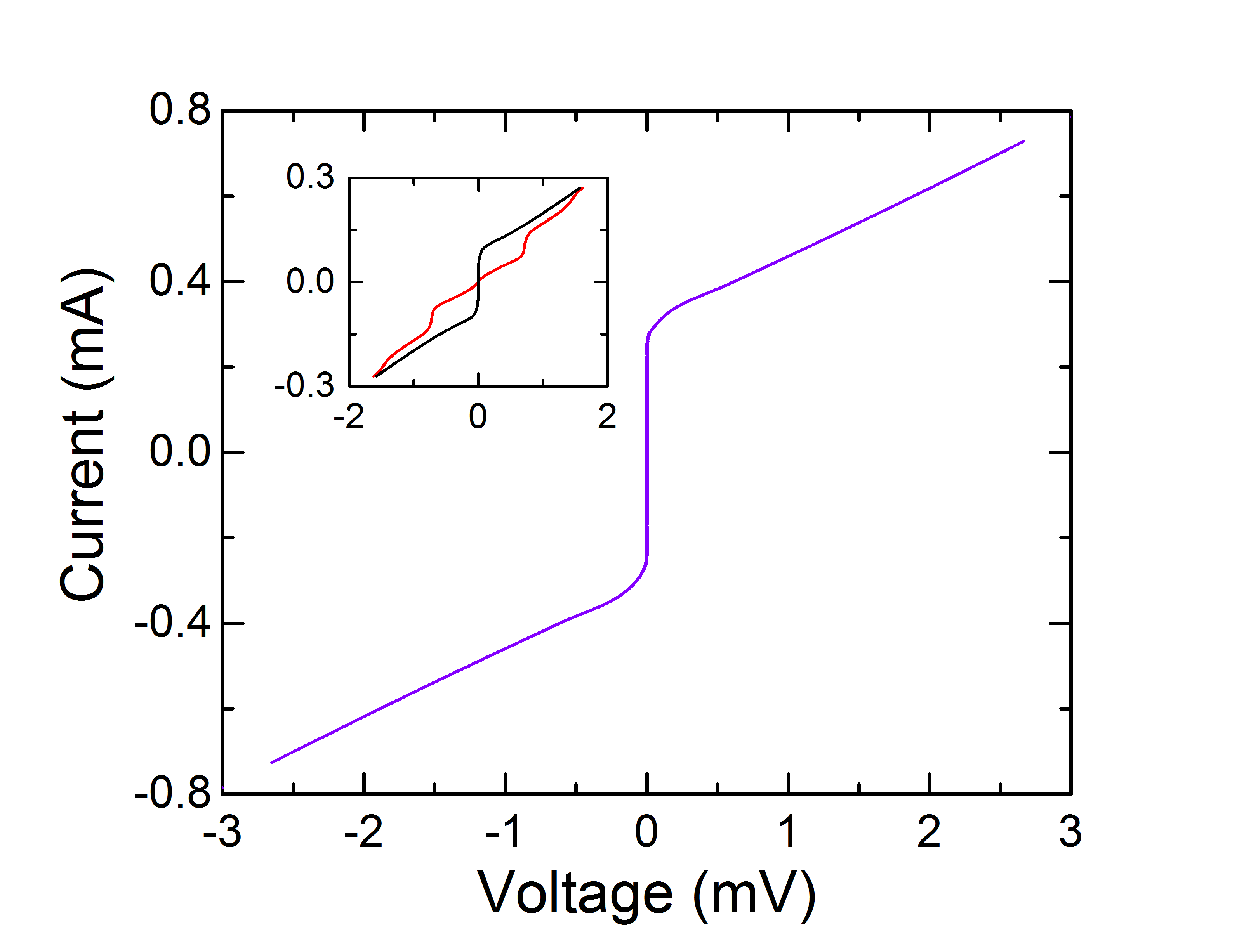
A series array of 20 SIS junctions was fabricated using a higher dose of irradiation. and Fig. 5(a) shows its I-V measured at 4 K. Like in the case of the SNS array the characteristics are smooth and resemble that of a single junction. However, we note that the resistance is 20 times higher than that of similarly fabricated single junction devices [13]. Due to limitations of our 4 K measurement setup we were unable to perform RF measurements for this chip to investigate Shapiro steps. However, because these are insulating barrier junctions we were able to investigate the quasiparticle tunneling spectrum. Using a lock-in amplifier the dynamic conductance of the array was measured at high voltage bias and the result is shown in Fig. 5(b). The large spike in the center is from the Josephson supercurrent and the peaks near 660 mV are attributed to the YBCO energy gap of all of the junctions. The energy gap of single HI-JJ using the same wafer of YBCO was previously measured to be 33 mV[13]. Here the array shows the same peak at 20 times the voltage assuring us that all 20 junctions are present with well formed insulating barriers.

III Conclusion
We have shown that by tuning the disorder density in HI-JJ it is possible to control the electrical properties of the junctions and create both SNS and SIS type junctions in YBCO. The helium ion beam offers great control over junction properties and uniformity which broadens the applications of ion irradiated junctions. Furthermore, direct writing of YBCO can also be utilized to combine junctions with nanowires [12] and nanostructured SQUIDs [15]. HI-JJ fabrication requires less process steps than prior-art techniques and can easily be scaled to a wafer process. With further process refinements HI-JJ could bring many applications of superconductive electronics out of the research lab and into the commercial sector.
Acknowledgment
The authors would like to acknowledge all the students in the lab for their passion about HTS electronics.
References
- [1] E. E. Mitchell, K. E. Hannam, J. Lazar, K. E. Leslie, C. J. Lewis, A. Grancea, S. T. Keenan, S. K. H. Lam, and C. P. Foley, “2D SQIF arrays using 20000 YBCO high josephson junctions,” Supercond. Sci. Technol., vol. 29, no. 6, p. 06LT01, 2016.
- [2] E. R. Pawlowski, J. Kermorvant, D. Crété, Y. Lemaître, B. Marcilhac, C. Ulysse, F. Couëdo, C. Feuillet-Palma, N. Bergeal, and J. Lesueur, “Static and radio frequency magnetic response of high superconducting quantum interference filters made by ion irradiation,” Supercond. Sci. Technol., vol. 31, no. 9, p. 095005, 2018.
- [3] B. J. Taylor, S. Berggren, M. O’Brien, M. C. de Andrade, and A. L. de Escobar, “HTS YBCO SQUID array transfer function dependence on inductance parameter,” in 2017 16th International Superconductive Electronics Conference (ISEC). IEEE, 2017, pp. 1–4.
- [4] S. Adachi, A. Tsukamoto, Y. Oshikubo, and K. Tanabe, “Fabrication of small biaxial high- gradiometric SQUID,” IEEE Trans. Appl. Supercond., vol. 26, no. 3, pp. 1–4, 2016.
- [5] B. Müller, M. Karrer, F. Limberger, M. Becker, B. Schröppel, C. J. Burkhardt, R. Kleiner, E. Goldobin, and D. Koelle, “Josephson junctions and SQUIDs created by focused helium-ion-beam irradiation of ,” Phys. Rev. Appl., vol. 11, p. 044082, Apr 2019. [Online]. Available: https://link.aps.org/doi/10.1103/PhysRevApplied.11.044082
- [6] W. E. Booij, A. J. Pauza, E. J. Tarte, D. F. Moore, and M. G. Blamire, “Proximity coupling in high- josephson junctions produced by focused electron beam irradiation,” Phys. Rev. B, vol. 55, pp. 14 600–14 609, Jun 1997. [Online]. Available: https://link.aps.org/doi/10.1103/PhysRevB.55.14600
- [7] A. E. White, K. T. Short, R. C. Dynes, A. F. J. Levi, M. Anzlowar, K. W. Baldwin, P. A. Polakos, T. A. Fulton, and L. N. Dunkleberger, “Controllable reduction of critical currents in YBa2Cu3O7-δ films,” Appl. Phys. Lett., vol. 53, no. 11, pp. 1010–1012, 1988. [Online]. Available: https://doi.org/10.1063/1.100652
- [8] S. S. Tinchev, “Investigation of RF SQUIDs made from epitaxial YBCO films,” Supercond. Sci. Technol., vol. 3, no. 10, pp. 500–503, oct 1990.
- [9] S. A. Cybart, Ke Chen, and R. C. Dynes, “Planar ion damage josephson junctions and arrays,” IEEE Trans. Appl. Supercond., vol. 15, no. 2, pp. 241–244, June 2005.
- [10] N. Bergeal, J. Lesueur, M. Sirena, G. Faini, M. Aprili, J. Contour, and B. Leridon, “Using ion irradiation to make high- josephson junctions,” J. Appl. Phys., vol. 102, no. 8, p. 083903, 2007.
- [11] S. A. Cybart, S. M. Wu, S. M. Anton, I. Siddiqi, J. Clarke, and R. C. Dynes, “Series array of incommensurate superconducting quantum interference devices from YBa2Cu3O7-δ damage josephson junctions,” Appl. Phys. Lett., vol. 93, no. 18, p. 182502, 2008. [Online]. Available: https://doi.org/10.1063/1.3013579
- [12] E. Y. Cho, Y. W. Zhou, J. Y. Cho, and S. A. Cybart, “Superconducting nano josephson junctions patterned with a focused helium ion beam,” Appl. Phys. Lett., vol. 113, no. 2, p. 022604, 2018.
- [13] S. A. Cybart, E. Y. Cho, T. J. Wong, B. H. Wehlin, M. K. Ma, C. Huynh, and R. C. Dynes, “Nano josephson superconducting tunnel junctions in YBa2Cu3O7-δ directly patterned with a focused helium ion beam,” Nat. Nanotechnol., vol. 10, no. 7, p. 598, 2015.
- [14] E. Y. Cho, M. K. Ma, C. Huynh, K. Pratt, D. N. Paulson, V. N. Glyantsev, R. C. Dynes, and S. A. Cybart, “YBa2Cu3O7-δ superconducting quantum interference devices with metallic to insulating barriers written with a focused helium ion beam,” Appl. Phys. Lett., vol. 106, no. 25, p. 252601, 2015.
- [15] E. Y. Cho, H. Li, J. C. Lefebvre, Y. W. Zhou, R. C. Dynes, and S. A. Cybart, “Direct-coupled micro-magnetometer with Y-Ba-Cu-O nano-slit squid fabricated with a focused helium ion beam,” Appl. Phys. Lett., vol. 113, no. 14, Oct 2018. [Online]. Available: http://par.nsf.gov/biblio/10076662
- [16] S. A. Cybart, S. M. Anton, S. M. Wu, J. Clarke, and R. C. Dynes, “Very large scale integration of nanopatterned YBa2Cu3O7-δ josephson junctions in a two-dimensional array,” Nano Lett., vol. 9, no. 10, pp. 3581–3585, 2009.
- [17] H. R. Yi, D. Winkler, and T. Claeson, “Tunneling through grain boundaries of YBa2Cu3O7-δ step-edge junctions,” Appl. Phys. Lett., vol. 68, no. 18, pp. 2562–2564, 1996.
- [18] W. Lang, M. Dineva, M. Marksteiner, T. Enzenhofer, K. Siraj, M. Peruzzi, J. Pedarnig, D. Bäuerle, R. Korntner, E. Cekan et al., “Ion-beam direct-structuring of high-temperature superconductors,” Microelectron. Eng., vol. 83, no. 4-9, pp. 1495–1498, 2006.